
Abstract
We report here the results of a study to understand the formation mechanism of single crystals of the transition metal chalcogenide, CuS, at the water–toluene interface through an interfacial reaction. Systematic measurements carried out using synchrotron x-ray scattering, electron microscopy, atomic force microscopy and calorimetric techniques clearly show that nano-crystallites of CuS form within a few minutes at the interface as the reagents are brought from the organic (upper) and aqueous (lower) layers to the interface, then crystallization of CuS proceeds over a few hours only by reorganization, despite the large excess available in both upper and lower liquid phases. The interface confinement and passivation by organics is critical here in the formation of single crystals having sizes of 6 and 200 nm along the normal and in-plane directions of the liquid–liquid interface.
Export citation and abstract BibTeX RIS
1. Introduction
Solution growth of free-standing nano-films of semiconductor crystals is of fundamental significance as quantum size effects become inherent in the two-dimensional structures [1–3]. Chemical reaction at the interface of two immiscible liquids is a natural choice to grow such free-standing anisotropic two-dimensional structures, as this process does not require the presence of a solid substrate. Growth of such nano-films at the organic–water interface has been demonstrated for metals and metal-chalcogenides by taking an organometallic precursor in the organic layer and the appropriate reagent in the aqueous layer [4–6]. The liquid–liquid interface based growth technique can be used effectively to produce such nano-films on a large scale and the method has several advantages over other conventional methods such as thermal evaporation, vacuum sputtering, laser deposition, metal–organic chemical vapor deposition (MOCVD) and molecular beam epitaxy (MBE). However, the ordering process involved in the formation of nano-films through such an interfacial reaction and the role of the liquid–liquid interface in this growth mechanism is not yet fully understood [7–10]. It has been shown recently that this growth process can be probed non-destructively using a high-energy synchrotron x-ray beam. This study could elucidate the formation of mono-dispersed 1.2 nm gold nanoparticles and the evolution of clustering of these nanoparticles as the thickness of the gold nanofilm increases at the water–toluene interface [10, 11]. It was shown earlier that, unlike clustering of gold nanoparticles, CuS formed in a similar water–toluene interfacial reaction are organized to produce single-crystalline nano-films [12]. Nano-structures of CuS find use in areas such as solar cells, cold cathodes and sensors, as CuS can exhibit metal-like properties [13–15]. Various preparation techniques, such as solid-state reaction [16], pyrolysis of single source precursors [17] and reaction in solutions [18], have been used to produce CuS on a large scale. CuS nano-rods have also been produced using well-defined molecular templates [19] formed in Langmuir–Blodgett structures [20, 21]. Here we report results of in situ x-ray reflectivity, electron microscopy, atomic force microscopy and calorimetry to understand the formation mechanism of nano-films of single-crystalline CuS at the water–toluene interface and its associated self-organization process [22, 23]. The results presented here show the formation of two-dimensional single crystals of CuS, having sizes of 6 and 200 nm along the normal and in-plane directions of the organic–aqueous interface.
2. Experimental section
2.1. Synthesis of CuS at interface
To prepare nano-films of CuS at the liquid–liquid interface, copper cupferronate, Cu(C6H5N2O2)2 or [Cu(cup)2], was used as the copper source in the toluene medium and Na2S as the sulfur source in the aqueous medium. In a typical preparation for carrying out x-ray scattering measurements, 60 ml of 0.24 mM Cu(cup)2 solution in toluene was slowly added to 14.5 ml of 3.74 mM Na2S in water taken in a sample cell (7 cm × 7 cm), as shown in figure 1. The CuS film forms only at the toluene–water interface and gradually turns green, while the two liquid phases remain colorless. In order to prevent the formation of Cu2S, an excess of Na2S was required. The molar ratio of Cu(cup)2 and Na2S is chosen as 1:4 for this experiment. The cell was mounted on an anti-vibration table to stabilize the interface for carrying out the x-ray measurements during the interfacial reaction at room temperature. For microscopy measurements this interfacial reaction was carried out in a glass beaker of similar volume and the reaction was stopped at different times by removing the upper toluene layer gently without disturbing the formed CuS nano-films. The nano-films could be lifted onto various substrates by means of forceps to enable electron microscopy and atomic force microscopy measurements.
2.2. X-ray scattering measurements
The in situ high-energy x-ray scattering study was carried out at the ID10B beamline of the European Synchrotron Radiation Facility (ESRF). The energy was set to 22 keV to allow the x-ray beam to pass through the upper toluene layer and probe the buried liquid–liquid interface. In figure 1 we have shown the schematic of the sample cell used for these measurements. The Teflon cell has two circular windows on diametrically opposite walls and two Kapton sheets of 25 μm thickness are fixed on both windows. It allows x-rays to go in and out of the cell and prevents liquid leakage during the scattering measurements. Two thin Si-wafers of equal heights were used near the entry and exit x-ray windows of the cell to anchor the water–toluene interface flat (refer figure 1). All the measurements were performed at room temperature (25 ° C) with varying incident beam sizes: 0.002 × 1.0 mm2 (V × H) from 0° to 0.2°, 0.02 × 1.0 mm2 from 0.2° to 0.5° and 0.1 × 1.0 mm2 up to 1.5° grazing angle of incidence, defined using conventional slits.

Figure 1. A schematic of a typical experimental Teflon cell (7 cm × 7 cm) and the scattering geometry. There are two circular windows on diametrically opposite walls of the cell. Two Kapton sheets of 25 μm thickness are fixed on both windows, allowing x-rays to go in and out of the cell and preventing liquid leakage during the scattering measurements. Two thin silicon wafers of equal heights were used near the entry and exit x-ray windows of the cell to anchor the water–toluene interface flat.
Download figure:
Standard image High-resolution imageIn the x-ray reflectivity technique, the scattered x-ray intensity normalized to the incident intensity is measured at very small grazing angles as a function of the vertical component of the wavevector qz while keeping the horizontal components qxy equal to zero. These measurements were carried out as a function of the reaction time by varying the grazing angles θi and θf (with θi = θf), while keeping the in-plane angle φ = 0 (refer figure 1). The reflectivity measurements provide us information about the electron density of the interfacial nano-films as a function of depth during the formation process. To obtain in-plane information of the interfacial nano-films, we carried out diffuse scattering measurements. A position sensitive detector (PSD) was used to collect the data as a function of the in-plane angle (φ), keeping the incident grazing angle (θi) fixed at 20 millidegrees. We also collected longitudinal diffuse scattering data in the same geometry with an offset of 0.2° in θf to find the background arising of reflectivity data. Scattering data in the same geometry from the toluene bulk were also collected by moving down the interface by 0.2 mm to obtain background data arising from bulk scattering. It should be mentioned here that for such measurements of the liquid surface and liquid–liquid interface, the x-ray beam is tilted using a crystal reflector and the sample cell is positioned by moving a goniometer vertically and horizontally to achieve appropriate scattering conditions, as shown in figure 1, as a liquid cell cannot be tilted like a solid surface.
2.3. Physiochemical characterizations
We have carried out transmission electron microscope (TEM) measurements using a FEI (Technai S-twin) microscope operating with an accelerating voltage of 200 kV. For TEM studies the film was lifted from the interface onto a holey carbon coated copper grid at various reaction times and high resolution (HRTEM) images, selected area electron diffraction (SAED) patterns and energy dispersive x-ray spectroscopy (EDS) data were taken for each sample. We used Gatan Digital Micrograph software for the analysis of the TEM images and SAED patterns. Scanning electron microscopy (SEM) images were also recorded with a Quanta 200 FEG microscope. Tapping mode atomic force microscope (AFM) experiments were carried out on samples lifted onto RCA cleaned Si-wafer surfaces using a Digital Instruments Nanoscope-IV, employing standard Si3N4 cantilevers. The height profile and particle distributions were obtained from atomic force microscopy images using WS × M software.
2.4. Calorimetric measurements
Isothermal titration calorimetry (ITC) measurements [24] were carried out using a VP-ITC micro-calorimeter to determine the nature of the reaction. Two identical coin shaped cells are enclosed in an adiabatic outer shield. Both cells were filled with the liquids during operation. The working volume of the cell is approximately 1.5 ml. The temperature differences between the reference cell and a sample cell are measured and it is calibrated to differential power (DP) units between the cells. This DP signal is used to maintain temperature equilibrium as the feedback power. Calibration of this DP signal is obtained by monitoring a known quantity of power through a resistive heater located on the cell.
In this study, we titrated 286 μl Cu(cup)2 toluene solution of different concentrations into 1.4 ml aqueous Na2S at a fixed molar ratio (1:4) to get the heat evolution or absorption during the reaction. We also titrated 286 μl pure toluene into 1.4 ml aqueous Na2S to measure the heat of dilution (control). In both cases we used the single injection mode (SIM) technique without stirring the solutions at room temperature (25 ° C). Here 'reaction' indicates the sum of the heat of dilution during mixing of two liquids and the heat during formation of chemical products (CuS) and 'control' means the heat of dilution of two liquids without any chemical reaction. The heat evolved during formation of CuS (enthalpy of CuS formation) is thus obtained from the difference of 'reaction' and 'control'.
3. Results and discussion
3.1. X-ray scattering results
In figure 2(a), we have presented measured and fitted reflectivity data. The reflectivity data of the water–toluene interface was measured before initiating the interfacial reaction and this data (Rf) was used to normalize all the other reflectivity data (R) measured as a function of reaction time. In figure 2(b), we show three representative R/Rf curves collected after the initiation of the reaction and the time of data collection are also indicated. The reflectivity curves were initially fitted with a model-independent procedure [25] and the obtained electron density profile (EDP) was then approximated with a box model having a minimum number of layers (two here) and interfacial roughness of the layers. In figure 2(c), we show the two layers as dashed lines and the roughness convoluted EDP as solid lines that closely represent EDPs obtained from the model-independent analysis. The solid fitted lines (red) shown in figures 2(a) and (b) are obtained with this two-box model [26]. The higher density box is assigned to the CuS layer and the lower density box just above water is assigned to the cupferronate layer that gets precipitated during the reaction. The thicknesses of the CuS and organic layers obtained are 6.5 nm, 5.3 nm, 5.6 nm and 8.4 nm, 7.9 nm, 9.1 nm after 18 min, 1 h 40 min and 2 h 57 min, respectively. The interfacial roughness values are found to be constant over the reaction time and we obtain roughness values to be 1.1 nm, 2.8 nm and 3.8 nm at the toluene–CuS, CuS–organic and organic–water interfaces respectively. Precipitation of the organic film between the CuS layer and water stops the reaction progressing further and the total film thickness between the toluene and water layers reaches a nearly constant value of 27 nm (see figure 2(c)).
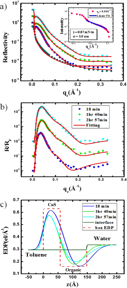
Figure 2. (a) Variation of in situ x-ray reflectivity data (R) as a function of qz after initiation of the chemical reaction at the toluene–water interface (blue: 18 min; green: 1 h 40 min; cyan: 2 h 57 min) and their fits (solid red lines). The reflectivity data (Rf) from a pure toluene–water interface (dark cyan) and its fit (solid red). Inset: the variation of diffuse scattering intensity due to CuS formation at the interface after 4 h 20 min as a function of qx at qz = 0.05 Å−1 (magenta) and the linear fit on a log–log scale (blue solid line). The data are shifted vertically for clarity. (b) The obtained R/Rf data as a function of qz for different reaction times and their fits (colors are same as in (a)). (c) The electron density profiles (EDPs) of the formed CuS–organic as a function of depth (z) between toluene and water at different times (corresponding colors as in (a)) and of the toluene–water interface (deep green) obtained from fitting the reflectivity data (refer text for details). The EDP of the simple two-box model (dashed red line) without roughness convolution is also shown.
Download figure:
Standard image High-resolution imageIn the inset of figure 2(a), we show a typical diffuse scattering intensity profile after subtracting the bulk toluene data as a function of qx by integrating the PSD data. We could determine [27] the effective interfacial tension and effective roughness of the toluene–water interface from the decay of intensity as  (where η is equal to
  , with γ as the interfacial tension) by fitting the straight line (blue line) shown in the log–log plot, giving η = 0.19. We get the interfacial tension value as 0.87 mN m−1, giving an effective roughness of 3 nm. It is to be noted here that this roughness value is similar to the value of organic–water roughness obtained from reflectivity analysis. The value of interfacial tension is much lower than that expected (27.8 mN m−1) for a pure toluene–water interface due to presence of the cupferronate. It is to be noted that the observed diffuse scattering profile is more complicated than the predicted straight line in the log–log plot for capillary waves, and the interfacial tension obtained is only an estimate.
3.2. Microscopy results
In figure 3, we show a representative result from our tapping mode atomic force microscopy (AFM) measurements. The height profile and histogram show the signature of two thicknesses, one at 12 nm and the other at 27 nm, measured from the top of the silicon substrate. The second peak at 27 nm gives the total film thickness and is consistent with the obtained x-ray results. The composite first peak indicates that the 27 nm film is generated by stacking of CuS and organic layers having various thicknesses.

Figure 3. (a) Tapping mode AFM image of CuS film, lifted onto a RCA cleaned Si-substrate after 3 h from the initiation of the reaction at the toluene–water interface. (b) Height profile of the CuS flowers along the line shown in (a), showing the average height of the film is about 27 nm. (c) Histogram of all the CuS flowers in (a), having two peaks at 12 and 27 nm.
Download figure:
Standard image High-resolution image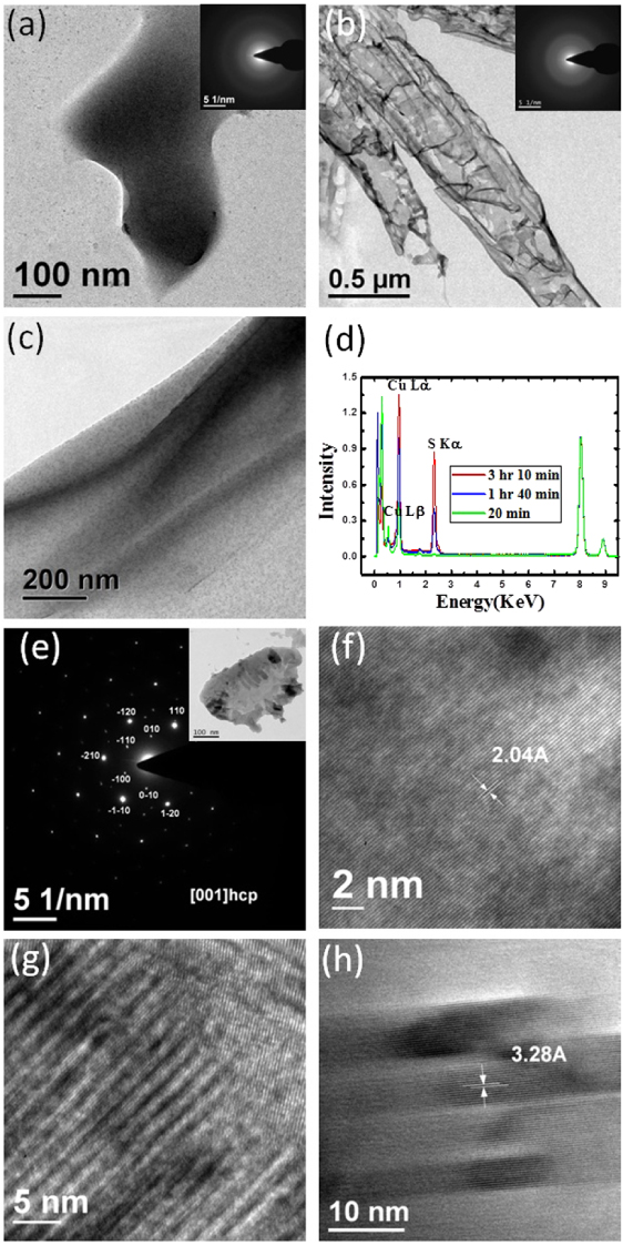
Figure 4. TEM images of CuS films obtained at the toluene–water interface by reacting 15 ml of 0.24 mM Cu(cup)2 toluene solution with 15 ml of aqueous 1.0 mM Na2S in a 8 cm diameter reaction vessel at 25 ° C for (a) 18 min and (b) 1 h 40 min, with the inset showing the corresponding diffuse SAED patterns. (c) A typical TEM image of a CuS nano-rod covered with organic products. (d) EDS data as a function of energy normalized with respect to the Cu Kα peak for the same CuS films at different times after the starting reaction (green: 20 min, blue: 1 h 40 min, red: 3 h 10 min). (e) Spot pattern in the SAED image obtained from the single-crystalline CuS film after 3 h 10 min from the initiation of the reaction. Inset: TEM image from which the SAED pattern was taken. (f) A typical HRTEM image of the CuS film has an interplanar spacing d of 2.04 Å, corresponding to the (008) plane of hexagonal CuS. (g) Moiré fringes of layered CuS films. (h) HRTEM image of an oriented nano-crystal shows a d spacing of 3.28 Å of the (100) plane of a hcp CuS crystal.
Download figure:
Standard image High-resolution imageIn figures 4(a), (b) and (e) we show typical transmission electron microscope (TEM) images and the corresponding selected area diffraction patterns (SAED) of CuS films obtained from the toluene–water interface at 18 min, 1 h 40 min and 3 h 10 min after initiation of the reaction. While the SAED patterns of the films obtained after 18 min and 1 h 40 min show diffuse rings, those obtained after 3 h 15 min exhibit sharp spots. The SAED patterns clearly reveal the gradual formation of the crystalline CuS film. The films are made of single-crystalline CuS and these crystals are essentially defect-free. The diffraction spots are indexed on the basis of the hexagonal structure (P63/mmc,a = 3.792 Å and c = 16.34 Å, JCPDF no. 06-0464). The crystallinity of the films increases with increasing reaction time.
Energy dispersive x-ray spectroscopic (EDS) data in figure 4(d) show the presence of Cu Kα, Lα, L β and S Kα lines. It is interesting that the normalized (with respect to Cu Kα) intensity of Cu Lα and S Kα increase continuously with the reaction time. Our x-ray reflectivity results (see figure 2(c)) clearly show that the CuS structures are embedded in the organic layers; we, therefore, monitored the lower energy Cu Lα and S Kα to probe the formation process. The binding of a large number Cu2+ and S2− ions initially form nano-crystals of CuS that remain embedded in organics and cannot exhibit diffraction spots. The intensity enhancement of Cu Lα and S Kα signals indicate that these tiny crystals aggregate to form large crystallites of CuS towards the organic surface through phase separation as the reaction time increases.
In figure 4(c), we show a typical TEM image of 'soft' composite films that form in the early phase of the reaction, showing the homogeneous presence of the cupferronate, (light) and CuS films (dark). These films show the presence of Cu Lα and S Kα signals, but no diffraction data in TEM. After about 3 h 10 min of reaction, the films start showing crystal formation, as indicated by the SAED pattern in figure 4(e) (inset: TEM image from which SAED pattern was taken). A typical high-resolution TEM image in figure 4(f) shows an interplanar spacing (d spacing) of 2.04 Å. This d spacing is close to the (008) interplanar spacing of hexagonal CuS. The moiré fringes (figure 4(g)) formed by interfering two sets of CuS lattice planes having nearly common periodicities. A high-resolution TEM image (figure 4(h)) shows collection of oriented nano-crystals, having a d spacing of 3.28 Å of the (100) plane of a hcp CuS crystal. These results show that small crystallites come together to form bigger crystallites, possibly through a 'contact epitaxy' process [28].
3.3. Proposed 3D model
Figures 5(a) and (b) show the large-scale organization of CuS nano-flowers exhibiting hexagonal in-plane ordering. Such films were obtained after about 2 h 15 min of the reaction. The inset in figure 5(a) shows the SAED pattern of these nano-flowers, confirming their polycrystalline nature. It is interesting that the average size crystallites obtained finally (figure 5(c)) are similar to those of nano-flowers. The electron density of CuS from reflectivity analysis remained at 0.63, compared with the expected bulk density of 1.294 electrons Å−3, suggesting a fractional occupancy of only 0.5 in a unit volume over the entire reaction time.
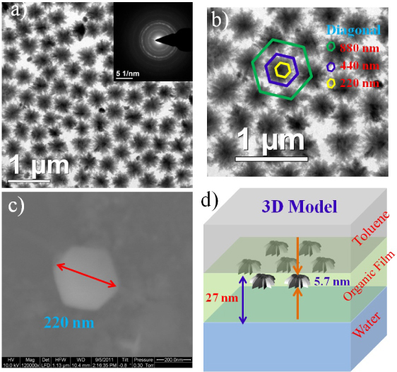
Figure 5. TEM image of (a) CuS nano-flowers obtained by reacting 15 ml of 0.24 mM Cu(cup)2 solution in toluene with 15 ml of 1.0 mM Na2S aqueous solution in a 8 cm diameter reaction vessel at 25 ° C for 2 h 15 min, with the inset showing rings in the SAED pattern. (b) Zoomed image of (a) showing hexagonal ordered CuS Nano-flowers. The size of the central dark portion of each flower (yellow hexagon) is almost 220 nm along the diagonal. (c) SEM image of hexagonal CuS crystal obtained from the toluene–water interface at same chemical condition after 12 h of the reaction, having a diagonal of 220 nm. (d) Three-dimensional schematic of the proposed model, involving disk-like CuS nano-flowers of 6 nm height and 220 nm diameter (mainly layered towards the toluene side) and an organic layer having a total thickness of 27 nm at the toluene–water interface (considering x-ray reflectivity as well as microscopy studies).
Download figure:
Standard image High-resolution imageIn figure 5(b), we show a 440 nm sized hexagonal box for one nano-flower, where only 220 nm is dark due to the presence of CuS. In figure 5(d), we show a simple model of such arrangements of the nano-flowers. Out of the cylindrical volume of length 27 nm and diameter 440 nm, the top 5.7 nm holds the nano-flowers with 0.5 fractional occupancy. The rest of the cylinder is occupied by cupferronate with an electron density of 0.16 electrons Å−3, about 40% of the value of the crystalline state. The number of CuS and cupferronate molecules in this model cylinder results as 6.0 × 10⁶ and 8.2 × 10⁶, respectively. This model calculation shows that almost all of the cupferronate molecules are near the water surface as a low-density spongy layer containing a large amount of pores and voids.
3.4. Calorimetric results
The obtained electron density profiles from x-ray reflectivity data clearly show that the amount of CuS crystals at the liquid–liquid interface remains constant for more than 3 h. Electron diffraction results shown in figure 4 clearly show that there is a growth in crystal size over this reaction time and the final crystal size (refer figure 5(c)) is similar to the size of the nano-flowers (refer figure 5(a)).
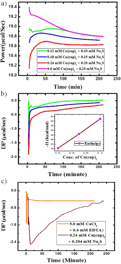
Figure 6. (a) Raw ITC single injection mode (SIM) data of heat evolution during the interfacial reaction (without stirring the liquids during or after injection) for different concentrations of titrates at 25 ° C. In an ITC cell: 1.4 ml water + Na2S; in an ITC syringe: 286 μl toluene + Cu(cup)2; the molar concentration ratio of Cu(cup)2 in toluene and Na2S in water for each titration is 0.12 mM:0.1 mM (green); 0.18 mM:0.15 mM (blue); 0.24 mM:0.2 mM (red) and 0.0 mM:0.2 mM (pink) for control (one of the titrant is missing). (b) Heat evolution curve due to CuS formation only at the interface (i.e. control subtracted heat evolution) during the respective titrations (bold green, blue, red solid lines, respectively) shown in (a). Inset: total heat evolution (enthalpy) of each titration for 3 h 15 min. (c) The resolution function (orange) of the ITC setup obtained for a standard binding reaction of 286 μl of 5.0 mM aqueous CaCl2 and 1.4 ml of 0.4 mM EDTA in mess-buffer. It clearly shows that the width of the resolution function is negligible with respect to a typical heat evolution curve (wine) obtained for the CuS formation process reported here.
Download figure:
Standard image High-resolution image
As a nano-crystal grows at the oil–water interface, three contributions to the interfacial energy, namely the particle–oil interface (γp/o), the particle–water interface (γp/w), and the oil–water interface (γo/w) change. ΔE due to the assembly of a single particle at the oil–water interface is given by [29]
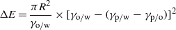
where R is the effective radius of the nanoparticle. In the present case, as the CuS crystals (size R) grow, we expect to see heat evolution over 3 h time. We carried out calorimetric measurement to probe this growth process. ITC measurements show that for each concentration of the reactants, heat evolution from the reaction during 3 h from the initiation of the reaction is different, and found to be higher for higher concentrations (figure 6(a)). In figure 6(b), we show the control (one of the titrants is missing, thereby no reaction occurs) subtracted heat for different concentrations with time, with the inset providing the enthalpy changes charactering the chemical reaction at three different concentrations of the titrants. Titration of 0.12 mM, 0.18 mM and 0.24 mM 286 μl of Cu(cup)2 in toluene with 0.10 mM (green), 0.15 mM (blue) and 0.20 mM (red) 1.4 ml of Na2S aqueous solution gives heats of 31 kcal mol−1,46 kcal mol−1 and 61 kcal mol−1 respectively. Figure 6(c) represents the resolution function (orange) of the ITC setup for a standard binding reaction with a typical heat evolution for CuS formation (wine).
4. Concluding remarks
In conclusion, we have shown here that the formation of CuS crystals at the aqueous–organic interface occurs through self-assembly of nano-crystallites, which are formed at the interface within a few minutes of reaction. In situ x-ray reflectivity measurements clearly show that thickness of the composite nanofilm remains around 27 nm over the entire reaction time, involving several hours, and the thickness of CuS rich layer remains around 6 nm. Atomic force microscopy measurements confirm the thickness of the film and its composite nature. Diffraction spots evolve over several hours as these nano-crystallites aggregate to form single crystals only through reorganization, despite the large excess available in both liquid phases. Calorimetric measurements reconfirm slow growth of the crystallites. The results presented here show that interface confinement, passivation by organics and the role of contact epitaxy [28] are critical in this growth process, which can produce the defect-free two-dimensional free-standing crystallites of CuS required for various possible applications.
Acknowledgments
SM, MKS and NV acknowledge the support of Department of Science and Technology, India for funding and support to carry out experiments at ESRF, France. We gratefully acknowledge the help of Professor D Ghose and A Metya with AFM measurements.