

Abstract
High purity SiO2 substrates were implanted by 45 keV Ti ions or sequentially implanted by 45 keV Ti and Cu ions at different fluences. After annealing at 900 °C, rutile TiO2 nanorods were synthesized in the samples sequentially implanted with Ti and Cu ions. Besides, strong room temperature exciton absorption was observed near the band edge of TiO2 in these samples. The position and intensity of the TiO2 exciton absorption peak can be regulated by changing the fluence of Ti and Cu ions. Finally, through analyzing the valence and distribution of elements of the samples, we put forward a possible mechanism about the formation of the surface polarized dipoles layer on the surface of TiO2 nanorods to explain the exciton-enhanced phenomenon. The experimental results provide an effective way to enhance the exciton absorption of TiO2, which could be used to fabricate more efficient optoelectronic devices.
Export citation and abstract BibTeX RIS
1. Introduction
Excitons are a kind of bound state by electron and hole attracted to each other by Coulomb interaction [1]. The exciton effect has an important influence on physical processes, such as light absorption, luminescence and optical nonlinearity in semiconductors [2–4], and there are some important applications, such as ultrashort pulse lasers, solid state quantum information and organic solar cells [5–7]. The exciton phenomena have been extensively investigated in some bulk materials, like GaN, GaP, ZnO, etc, as their large exciton binding energy allows them to be retained at room temperature [8–10].
As an important semiconductor material, TiO2, has been widely used in photocatalysts, solar cells, ultraviolet light shielding, and so on. However, the excitons in bulk TiO2 belong to weakly bound ones due to effective electronic screening effects, and it has a low exciton binding energy of about 4 meV [11]. They could automatically dissociate to electrons and holes at room temperature ( meV), resulting in a very short exciton lifetime. Therefore, exciton absorption is feeble and cannot be easily observed in bulk TiO2 at room temperature. In the past few decades, with the development of low-dimensional quantum materials, it was found that lots of one-dimensional (1D) and two-dimensional (2D) materials exhibit higher exciton binding energy than the corresponding bulk materials [12–14]. In fact, for low dimensional semiconductor quantum structures, the activity of carriers is limited in some dimensionalities, which greatly increases the cloud overlap between the holes and electrons, resulting in the enhancement of the Coulomb binding energy and oscillator strength. Therefore, the quantum binding effect could cause enlargement in exciton binding energy [15, 16]. However, as far as we know, there are no reports paying close attention to the change of exciton absorption in low dimension TiO2 materials, as the changes are not evident in most cases. Besides, TiO2 is also widely used in dye-sensitized solar cells for the electron transport layer and blocking layer to prevent recombination [17]. If the retention capacity of the excitons in TiO2 can be enhanced, TiO2 can be used as electron generation and conduction materials simultaneously, which may enhance the power conversion efficiency (PCE) of the solar cell effectively.
In this paper, the method of Ti and Cu ion sequential implantation was used to synthesize the samples with TiO2 nanorods. These samples produce significant exciton absorption peak at room temperature. Besides, it is found that the intensity of the exciton absorption is enhanced with increasing the fluence of Ti ions, and rising the fluence of Cu ion could cause a significant red shift of the exciton absorption. We consider the fact that the mechanism of exciton absorption enhancement should be concerned with the formed dipoles on the surface of the TiO2 nanorods when Cu ions were introduced into the samples. It should be related to oxygen migrating from the high oxygen density material (TiO2) to the low one (CuO), leading to the generation of dipoles between vacancies at the surface of TiO2 and electrons from O− in CuO. Our findings provide an effective route to improve the exciton absorption of TiO2 at room temperature, which is beneficial for TiO2 applied to some new types of solar cells, such as dye-sensitized solar cells and perovskite solar cells.
2. Experimental
2.1. Synthesis of samples
Optical-grade amorphous silica slices with a thickness of 1 mm were implanted by 45 keV Ti ions to fluences of 2.0 × 10¹⁷, 1.5 × 10¹⁷ and 1.0 × 10¹⁷ ions cm−2, respectively. Subsequently, some Ti ion implanted samples were implanted with 45 keV Cu ions to fluences of 3.0 × 10¹⁶ and 5.0 × 10¹⁶ ions cm−2, respectively. The implantation was carried out by using a metal vapor vacuum arc (MEVVA) implanter. In order to avoid overheating on the host matrix, the flux density was kept below 4.0 µA cm−2 during implantation. Moreover, the target plate was designed to rotate at a stabilized speed of 5 rpm to maintain the uniformity of implantation. The implantation parameters as well as the names of the prepared samples are summarized in table 1. After implantation, all the prepared samples were furnace annealed in N2 atmosphere at 900 °C for 6 h.
Table 1. Names and implantation parameters of all the samples.
| Sample names | Ti1 | Ti1.5 | Ti2 | Ti1+Cu3 | Ti1.5+Cu3 | Ti2+Cu3 | Ti2+Cu5 | |
|---|---|---|---|---|---|---|---|---|
| Fluence of ions (ions cm−2) | Ti | 1.0 × 10¹⁷ | 1.5 × 10¹⁷ | 2.0 × 10¹⁷ | 1.0 × 10¹⁷ | 1.5 × 10¹⁷ | 2.0 × 10¹⁷ | 2.0 × 10¹⁷ |
| Cu | — | — | — | 3.0 × 10¹⁶ | 3.0 × 10¹⁶ | 3.0 × 10¹⁶ | 5.0 × 10¹⁶ | |
2.2. Characterization
Optical absorption (OA) spectra of the samples were measured with a HITACHI double-beam spectrophotometer (UV-3600PC) with wavelengths from 200 to 800 nm. The scanning interval and the bandwidth were 0.1 nm and 2 nm, respectively. The photoluminescence (PL) spectra were recorded with HOR1BA JOB1N YVON Fluorolog 3 fluorescence spectrophotometer in the range from 360 nm to 620 nm with an excitation wavelength of 330 nm. The surface morphologies of the samples were investigated by Bruker MultiMode 8 atom force microscope (AFM) in the tapping mode. The chemical states of elements of the samples were determined by x-ray photoelectron spectroscopy (XPS) using a VG ESCALAB MKII x-ray photoelectron spectrometer (VG Scienta, USA) with Mg Kα radiation (λ = 9.89 Å). The shape, size and distribution of the formed nanostructures were characterized by a Tecnai G2 F20 S-Twin transmission electron microscope (TEM), equipped with energy disperse x-ray spectroscopy (EDXS) operating at an accelerating voltage of 200 kV.
3. Results and discussion
Figure 1(a) shows the OA spectra of the prepared samples before and after annealing. One can find from the figure that there is no distinct band edge corresponding to TiO2 for the as-implanted Ti2 sample. Similar spectra have also been detected in the as-implanted Ti1 and Ti1.5 samples except for slight differences in absorption intensity (not shown here). After annealing, a clear absorption band edge at 3.4 eV (364.7 nm) appears in the Ti2 sample, which means that the implanted Ti atoms have been oxidized to TiO2 [18]. For the as-implanted Ti+Cu samples, although post Cu ion implantation could change the absorption intensity, the shape of absorption spectrum nearly stays unchanged. However, after annealing, it can be found that the OA spectra of the Ti+Cu samples show a distinct red-shift compared with the Ti2 sample, which should mainly be ascribed to the doped Cu ions, as the Cu doped TiO2 would alter the energy band structure and introduce impurity states [19]. It should be noted that all the Ti+Cu3 samples produce a distinct absorption peak around 339 nm, which should be attributed to the exciton absorption of TiO2 [20, 21]. Besides, with the increase in the fluence of Ti ions, the intensity of the exciton absorption peak gradually becomes stronger, while the wavelength is unaltered. Comparing the absorption spectra of the Ti2+Cu3 and Ti2+Cu5 samples, one can see that the intensity of the exciton peak changes little, but the red-shift comes out as the fluence of Cu ions increases. So, we can conclude that the intensity of the exciton absorption is related to the fluence of Ti ions, and it strengthens with increasing the fluence of Ti ions. Furthermore, the wavelength of the exciton peak is concerned with the fluence of Cu ions, which causes a red-shift of the exciton absorption peak when increasing the amount of doped Cu ions in TiO2. Finally, from figure 1(a), it can also be found that a weak absorption peak occurs at about 580 nm in the Ti2+Cu5 sample as shown by the arrow, which should be attributed to the surface plasmon resonance (SPR) absorption of Cu nanoparticles [22]. The results suggest that some of Cu nanoparticles have not completely oxidized into CuO even after annealing at high temperature.

Figure 1. (a) OA spectra of the prepared samples before and after annealing. (b) PL spectra of the samples after annealing. The inset shows the Gaussian curve fitted PL spectrum of the Ti2+Cu3 sample.
Download figure:
Standard image High-resolution imageFigure 1(b) gives the PL spectra recorded in some annealed samples. It is clear that the luminescence band appearing in the Ti2 sample is very weak. However, two luminescence bands occur in all the Ti+Cu samples, which are situated in wavelength ranges of 370–500 and 520–620 nm, respectively. The emission band at 520–620 nm should be attributed to oxygen vacancies in TiO2 [23], which may be induced by Cu ion implantation, while the emission band at 370–500 nm could be deconvoluted into three emission peaks. As an example, the Gaussian curve fitted PL spectrum of the Ti2+Cu3 sample is inserted in figure 1(b), from which one can clearly see that three emission peaks are centered at about 394, 425 and 460 nm, respectively. The peak at 394 nm should be ascribed to the radiation of self-trapped excitons [24, 25], The other two peaks at 425 and 460 nm result from the surface states as well as the shallow and deep surface traps associated with the Ti3+ states [26, 27]. The results show that all the Ti+Cu samples produced significant exciton emission.
Figure 2 shows the AFM images of some prepared samples before and after annealing. Similar flat surface morphologies have been observed in all the samples before annealing, so only the Ti2 sample is taken as an example. One can see from figure 2(a) that the surface of the as-implanted Ti2 sample is nearly flat with a few tiny pits, and the root mean square roughness is about 2.21 nm. After annealing, the surface of the Ti2 sample shows a lot of particles with the size of tens of nanometers, as shown in figure 2(b). However, large amounts of TiO2 nanorods appear on the surface of all the Ti+Cu samples after annealing. The surface morphology of the Ti1+Cu3 sample has been modified clearly after implantation of Cu ions. A mass of shorter nanorods generated on the surface of the sample can be seen, but due to the lower fluence of Ti ions, the nanorods are smaller in size; about 150 nm, while in the Ti1.5+Cu3 and Ti2+Cu3 samples, the size of the nanorods becomes larger. Comparing the three samples, it is revealed that as the fluence of Ti ions increases, the size and volume of TiO2 nanorods are also augmented. The surface morphology of the Ti2+Cu5 sample is exhibited in figure 2(f). Although the fluence of Cu ions in the Ti2+Cu5 sample is different from that in the Ti2+Cu3 sample, the uniform fluence of Ti ions results in similar surface morphology with almost the same length of nanorods.
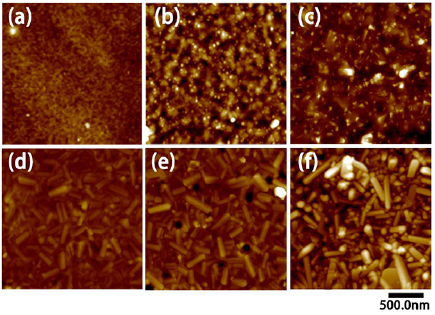
Figure 2. AFM images of (a) Ti2 sample before annealing, and (b) Ti2, (c) Ti1+Cu3, (d) Ti1.5+Cu3, (e) Ti2+Cu3, (f) Ti2+Cu5 samples after annealing.
Download figure:
Standard image High-resolution imageThe XTEM results of the Ti2+Cu3 sample after annealing are shown in figure 3. The Ti2+Cu3 sample consists of a single layer TiO2 nanorods on the shallow surface with a depth of about 100 nm. Besides, some small TiO2 nanoparticles still exist in deeper positions under the nanorods. From the SAED pattern shown in figure 3(b), one can find that the nanorods are mainly composed of rutile TiO2 with a polycrystalline structure. Figure 3(c) exhibits the high-resolution TEM (HRTEM) image of one nanorod on the surface. From the image, one can find that the interplanar spacings are 0.327 and 0.457 nm, corresponding to the crystal faces of (1 1 0) and (1 0 0) of rutile TiO2, which is consistent with the SAED patterns.
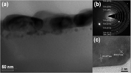
Figure 3. (a) XTEM results of TiO2 nanorod layers in the Ti2+Cu3 sample after annealing, (b) the SAED patterns of the Ti2+Cu3 sample, and (c) high-magnification HRTEM image of one nanorod.
Download figure:
Standard image High-resolution imageFigure 4 depicts the XPS spectra of the Ti2 and Ti2+Cu3 samples after annealing. The Ti 2p spectrum of the Ti2 sample in figure 4(a) shows two distinct peaks at 464.0 eV (Ti 2p1/2) and 458.3 eV (Ti 2p3/2) corresponding to Ti4+ species. While the XPS spectrum of the Ti2+Cu3 sample shows a clear deformation in the direction of lower binding energy. After deconvolution, the Ti 2p spectrum of the Ti2+Cu3 sample could be divided into two components of each peak, in which the emerging new peaks at 463.1 eV and 457.4 eV correspond to Ti3+ species [28]. Moreover, the components fitting from the Cu 2p spectrum at 953.0 eV (Cu 2p1/2) and 933.2 eV (Cu 2p3/2) and the satellite peak at near 943.8 eV confirm the existence of Cu2+ species, as shown in figure 4(b) [29, 30]. It could be found that due to the existence of Cu ions, a large number of Ti3+ ions are introduced into the Ti2+Cu3 sample. During annealing in N2 atmosphere, most of the defects induced by implantation may be repaired, and the defects inside TiO2 would disappear mostly in the growth of TiO2 nanorods. So, these Ti3+ should be associated with the Cu2+ existing in TiO2 nanorods or be generated on the surface of the TiO2 nanorods.

Figure 4. (a) XPS spectra of Ti 2p core level of the Ti2+Cu3 and Ti2 samples with the fitting results. (b) XPS spectrum of Cu 2p core level of the Ti2+Cu3 sample.
Download figure:
Standard image High-resolution imageTo gain an insight into the distribution of elements in the nanorods, the HADDF image of one nanorod with the corresponding Ti and Cu elemental color mappings is presented in figure 5. It can be found in figure 5(b) that the Ti element is mainly distributed in the TiO2 nanorods and some small nanoparticles below the nanorods layer, while the Cu element shown in figure 5(c) has a wide distribution range including exterior and interior of the TiO2 nanorods, which is larger than the ion range of Cu ions (38.4 ± 13.2 nm according to simulations by using SRIM2013 code [31]). Such a wide Cu distribution could be due to the thermal diffusion of Cu during annealing at high temperatures [32, 33]. The line scanned average atomic-number profiles of Cu and Ti were carried across the red line on the cross-sectional area in figure 5(a). As shown in figure 5(d), with the growth of TiO2 nanorods, some Cu ions remain inside them. Especially, it should be noted that the distribution of the Cu element is significantly higher in the edge portion of TiO2 nanorods than the substrate and interior of nanorods, suggesting that a large number of Cu ions are concentrated on the surface of TiO2 nanorods, which is also consistent with the distribution of the Cu element in figure 5(c). In addition, although some TiO2 nanoparticles still exist under the TiO2 nanorods, the Cu ion distribution density in these parts does not increase, as shown in figure 5(c).

Figure 5. (a) HAADF image of the Ti2+Cu3 sample after annealing, (b) and (c) EDXS element color mappings for Ti and Cu element, (d) the line-scanned average atomic-number profiles of Cu and Ti across one nanorod of TiO2 nanorods on the surface.
Download figure:
Standard image High-resolution imageIn fact, the TiO2 nanorods structure prepared by other methods by the hydrothermal method or chemical vapor deposition (CVD) did not produce such strong exciton absorption at room temperature in previous literature [34–36]. Therefore, it is convincing that the cause of exciton absorption cannot simply be attributed to the formation of TiO2 nanorods. Besides, the quantum effect could be neglected in these samples as the diameter of the TiO2 nanorods produced in our samples is several tens or even hundreds of nanometers. However, unlike previous research, a large amount of Cu ions aggregates on the surface of the TiO2 nanorods in the Ti+Cu samples in the form of CuO. So, we could make a reasonable hypothesis that the strong exciton absorption may be related to the presence of these Cu oxides.
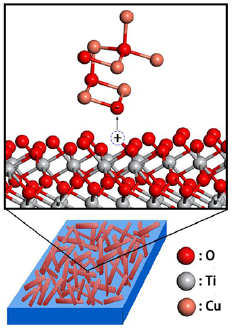
Since the presence of copper oxides will fiercely promote the growth of TiO2 during the annealing process [37], and it will accumulate a certain amount of CuO on the surface of TiO2 nanorods with their growth. Then the dipoles could appear in the interface between the two high-k material, as the TiO2 and CuO own different electronegativities (χ) and oxygen areal densities (σ) [38]. As shown in figure 6, a possible explanation is given as when the two dielectric materials are in contact, oxygen would migrate from the higher oxygen density material to the lower one. The calculated oxygen areal density ratio at the interface for the two materials could be expressed as [38, 39]

where  and
and  represent the volume of the structure including a oxygen atom in TiO2 and CuO, respectively. They could be calculated by analyzing their structures and the values are 15.61 Å3 and 19.98 Å3, respectively. The calculated result of the oxygen areal density ratio is 1.18, which is larger than 1. This could bring about positively charged vacancies at the surface of TiO2 and dipoles between TiO2 and CuO, which also led to a large number of Ti3+ arising at the interface of TiO2 nanorods [20]. The large number of dipoles on the surface of TiO2 can be a trap center of excitons and greatly strengthen the surface exciton binding energy; the Coulomb interaction between the surface electrons and holes of TiO2 nanorods and CuO in other words [40], and the presence of abundant TiO2 nanorods in the samples provides enough space for the formation of the dipoles layer. It has been reported that the exciton binding energy of surface state is much higher than that in bulk semiconductor [41, 42]. For nanoscale materials, surface exciton binding energy would intensely affect the exciton effect, due to the enhancement of surface effect, while the formation of the interface dipoles is an efficient method to enhance the surface exciton binding energy, which can be regarded as the trap center of excitons [21]. Therefore, the strong exciton absorption in the Ti+Cu samples could be attributed to the formation of interfacial dipoles layer on the surface of TiO2 nanorods. Besides, the assembly progress of TiO2 nanorods also plays a part on efficient exciton collectors [43]. Another important point is that some defects existing on the surface of TiO2 could inevitably deform the interface of TiO2, and this may also become a kind of self-trapping excitons center [21]. Based on the above points, the Ti+Cu samples could have a stronger exciton binding energy and enhance exciton absorption compared with samples without Cu ions implanted.
Figure 6. Schematic representation of migration of O ion and formation of dipoles on the surface of TiO2 nanorods and CuO nanoparticles.
Download figure:
Standard image High-resolution image
In addition, there is almost no change in the position of the exciton absorption peak as the fluence of Ti ions increases. As with the volume of TiO2 nanorods distinctly increasing, more Cu oxides could accumulate on the surface of TiO2, which also subjoins more contact area with CuO on the surface, thereby raising the number of surface dipoles, resulting in an enhancement in exciton absorption intensity. Although the TiO2 nanoparticles have a larger specific surface area, the distribution of the Cu element is relatively dispersed around them. Compared with the Ti2+Cu3 and Ti2+Cu5 samples, the exciton absorption peaks show distinct red shift when the fluence of Cu ion increases. The main reason should be related to the increase of doping content of Cu, which could cause a different red-shift level of the exciton peak [44, 45]. Besides, as the surface morphology of Ti2+Cu3 and Ti2+Cu5 samples are analogical, the number of surface polarized dipoles would be similar, so the intensities of exciton absorption peaks are alike. Finally, it should be mentioned that the Zn+Ti samples prepared in a similar way could also produce evident exciton absorption [46]. We consider that the appearance of the exciton absorption could be attributed to the generation of dipoles between ZnO and TiO2 nanorods in a similar way.
4. Conclusion
In summary, the TiO2 nanorods were synthesized by Ti and Cu ion sequential implantation and subsequent annealing. The Ti+Cu series samples produce distinct exciton absorption peaks at room temperature. Besides, it gradually becomes stronger with increasing the fluence of Ti ions, and when the fluence of Cu ions increases, the exciton absorption peak produces a significant red-shift. The reason could be due to the movement of oxygen from the TiO2 (larger σ) side to the CuO (smaller σ) side on the surface of the TiO2 nanorods. The generated surface polarized dipoles could enhance the surface exciton binding energy efficiently, and the exciton absorption of the Ti+Cu samples is greatly enhanced. Besides, the novel and simple method can control the intensity and position of exciton absorption in visible light significantly, which may be beneficial for applications on solar cells.
Acknowledgments
This work was supported by the Natural Science Foundation of China (NSFC) (Grant Nos. 11675120, 11535008).