

Abstract
The construction of two-dimensional (2D) van der Waals (vdW) heterostructures is an effective strategy to overcome the intrinsic disadvantages of individual 2D materials. Herein, by employing first-principles calculations, the electronic structures and potential applications in the photovoltaic field of the β-In2X3/α-In2X3 (X = S and Se) vdW heterostructures have been systematically unraveled. Interestingly, the band alignments of β-In2S3/α-In2S3, β-In2Se3/α-In2Se3, and β-In2Se3/α-In2S3 heterostructures can be transformed from type-I to type-II by switching the polarization direction of α-In2X3 layers. It is highlighted that the light-harvesting ability of the β-In2X3/α-In2X3 vdW heterostructures is significantly higher than the corresponding monolayers in nearly the entire visible light region. Interestingly, type-II β-In2S3/α-In2Se3↓ heterostructure can achieve the power conversion efficiency of 17.9%, where the α-In2Se3 layer acts as a donor and the β-In2S3 layer displays as the acceptor. The present research not only provides an in-depth understanding that the out-of-plane polarization of α-In2X3 monolayers can efficiently modulate the band edge alignment of the β-In2X3/α-In2X3 vdW heterostructures, but also paves the way for the application of these heterostructures in the field of photovoltaics and optoelectronics.
Export citation and abstract BibTeX RIS
1. Introduction
The detection of graphene [1] has sparked a growing fascination with the investigation of two-dimensional (2D) materials, leading to the swift advancements of 2D materials [2–4]. Since then, a large number of 2D materials have been experimentally synthesized or theoretically predicted, including but not limited to silicene [5], black phosphorene (BP) [6, 7], transition metal carbides/nitrides [8–11], transition metal chalcogenides [12–15], and group III metal chalcogenides (MX and M2X3) [16–21]. In addition, the construction of van der Waals (vdW) heterostructures enlarges the 2D material families [22–24]. Compared with single-layer 2D materials, the properties of 2D vdW heterostructures can be efficiently designed according to particular requirements, which makes them more useful and flexible in the applications of photovoltaic and optoelectronic devices [25, 26]. There are three types of band edge alignments in 2D semiconductor/semiconductor vdW heterostructures, each of which can be applied in different fields. The type-I heterostructures are commonly used in light-emitting diodes [27] and lasers [28], type-II heterostructures are suitable for photocatalysis [29, 30] and photodetectors [31], and type-III can be employed in tunneling field-effect transistors [32]. Therefore, designing vdW heterostructures with specific functions has become an emerging platform for developing innovative photovoltaic and optoelectronic devices.
Recently, a category of semiconducting 2D In2X3 (X = S, Se, and Te) monolayers has gained increasing attention due to their fascinating properties [33–35]. The 2D In2X3 monolayers have two distinct phases known as α-In2X3 and β-In2X3, and several of them have been successfully synthesized in experiments, such as α-In2Se3 [36–38] and β-In2X3 (X = S, Se and Te) [18, 39–41]. Among them, the β-In2X3 monolayers exhibit high photoresponsivity and light absorption and show great potential applications in photodetectors [42] and solar cells [43, 44]. On the other hand, the out-of-plane electric polarization arising from the asymmetric structure of α-In2X3 monolayers provides an efficient way to tune the electronic structures of the α-In2X3-based vdW heterostructures [45–52]. Therefore, systematic investigation of the out-of-plane electric polarization effect on the electronic structures of the β-In2X3/α-In2X3 vdW heterostructures and unraveling their further applications in photovoltaic and optoelectronic fields are meaningful and of great interest.
This work comprehensively studies the structural, electronic, band alignments, and optical properties of the β-In2X3/α-In2X3 vdW heterostructures based on density functional theory (DFT) calculations. The ab initio molecular dynamics (AIMD) simulations demonstrate the thermal dynamic stabilities of the β-In2X3/α-In2X3 vdW heterostructures. By switching the out-of-plane polarization direction of α-In2X3 layers, the band edge alignment features of β-In2S3/α-In2S3, β-In2Se3/α-In2Se3, and β-In2Se3/α-In2S3 heterostructures can be tuned from type-I to type-II. Moreover, the β-In2Se3/α-In2S3↓ heterostructure is suitably used as a solar cell with a PCE of 17.9%. Our results shed light on the effect of out-of-plane polarization direction of α-In2X3 layers on the electronic structures of the β-In2X3/α-In2X3 vdW heterostructures and offer new insight into designing advanced electronic devices based on 2D In2X3-based vdW heterostructures.
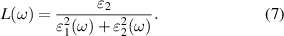
2. Computational details
The present works were based on the DFT implemented in the Vienna ab initio Simulation Package (VASP) [53]. The projector-augmented wave method [54] was used to describe the interactions between valence and core electrons, while the generalized gradient approximation, as parameterized by Perdew-Burke-Ernzerhof [55] was used to treat exchange-correlation functional effects. The cutoff energy for the plane-wave basis set was set to 500 eV, and an 11 × 11 × 1 k-points grid was used for the Brillouin zone sampling. The energy and force tolerance convergence criteria were set to 10−6 eV and 0.01 eV Å−1. The Heyd-Scuseria-Ernzerhof hybrid functional (HSE06) [56] was used to correct the band structures and band edge alignments of heterostructure and monolayer systems. A vacuum layer of at least 20 Å were added along the z-direction. For the α-In2X3 monolayers and β-In2X3/α-In2X3 vdW heterostructures, using the center of mass as the reference point, the Berry phase [57, 58] expressions with dipole correction are applied to these systems, which allows for the adjustment of the misalignment between the vacuum levels on the different sides of the structures. The DFT-D3 approach [59, 60] was utilized to account for vdW interactions. AIMD [61] simulations were performed using a canonical ensemble regulated by the Nose-Hoover thermostat [62] to examine the thermodynamic stability of heterostructures. The VASPKIT code [63] was used to post-processing some VASP calculation results.
The formation energy (Ef) and binding energy (Eb) of the β-In2X3/α-In2X3 heterostructures can be defined as follows:


where  ,
,  ,
,  are the total energies of β-In2X3/α-In2X3, β-In2X3 and α-In2X3, respectively.
  and
and  represent the total energies of β-In2X3 and α-In2X3 monolayer fixed in the corresponding heterostructures lattice constant, respectively, and A is the cross-sectional area. In 2D vdW heterostructure, the formation energy refers to the energy changing of forming certain vdW heterostructure, which represents the energy difference when stacking two independent 2D materials to create the heterostructure. The formation energy can be used to assess the stability of the heterostructure, where a more negative value of formation energy indicates the structure is more stable. On the other hand, the binding energy reflects the binding strength between two layers of the heterostructure. Thus, the more negative value of binding energy indicates the stronger interaction between two layers in heterostructures. Herein, the formation energy includes the binding energy and additional lattice distortion energy.
3. Results and discussions
Prior to constructing the β-In2X3/α-In2X3 (X = S and Se) heterostructures, we initially investigated the corresponding monolayers. The atom structures of α-In2X3 and β-In2X3 monolayers are shown in figures S1(a) and (b), respectively. Both the β-In2X3 and α-In2X3 monolayers belong to the trigonal 2D lattice with space groups of  and
and  , respectively, and possess 5 atomic layers with the X-In-X-In-X stacking configuration. After the structures are fully relaxed, the lattice constants are estimated to be 3.84, 4.01, 3.93, and 4.10 Å for β-In2S3, β-In2Se3, α-In2S3, and α-In2Se3 monolayers, respectively. Due to the asymmetric structure of the α-In2X3 monolayers, the out-of-plane electric polarization will be produced, pointing from the upper chalcogenide atoms to the bottom chalcogenide atoms, as marked by the red arrow in figure S1(b). On the one hand, the electric polarization in the α-In2X3 monolayers will lead to inhomogeneous charge distribution, generating a built-in electric field, which can facilitate the separation of photogenerated carriers. On the other hand, the built-in electric field will result in the existing electrostatic potential difference between the two surfaces of the α-In2X3 monolayers. Therefore, two different band alignments of the energy bands will be generated with respect to the vacuum levels on the different surfaces of α-In2X3 monolayers. It should be noted that the polarization orientation of α-In2X3 monolayers can be reversed via the application of external electric field. The band structures illustrated in figures S1(c) and (d) were used to understand the electronic structures of β-In2X3 and α-In2X3 monolayers. It can be seen that all of them pertain to indirect band gap semiconductors. The calculated band gaps of β-In2S3, β-In2Se3, α-In2S3, and α-In2Se3 monolayers by using HSE06 functional are 1.97 eV, 1.2 eV, 2.15 eV, and 1.41 eV, respectively. It should be noted that the obtained lattice constants and band gaps of the α-In2X3 and β-In2X3 monolayers match the previous experimental and theoretical results very well [33, 39, 40, 64], providing evidence of the validity of these theoretical predictions.
Based on the four monolayers mentioned above, we have constructed four different heterostructures by perpendicularly combing one β-In2X3 layer and one α-In2X3 layer together, namely β-In2S3/α-In2S3, β-In2Se3/α-In2Se3, β-In2Se3/α-In2S3 and β-In2S3/α-In2Se3 heterostructures, the corresponding lattice mismatches are 2.12%, 2.21%, 2.11%, and 6.31%, respectively. It is noted that β-In2S3/α-In2Se3 heterostructure can be fabricated despite the relatively large lattice mismatch between β-In2S3 and α-In2Se3, since both the β-In2S3 and α-In2Se3 monolayers exhibit outstanding mechanical characteristics [65, 66]. Due to the different out-of-plane polarization states of the α-In2X3 monolayers, we denote the heterostructure formed by the connection of β-In2X3 and α-In2X3 in the downward polarization direction as the β-In2X3/α-In2X3↓ heterostructure, while connection in the upward polarization direction as the β-In2X3/α-In2X3↑ heterostructure. Three distinct stacking configurations were employed as an initial criterion to examine how the stacking patterns influence the stability of heterostructures with different polarization states, as depicted in figures 1(a) and (b). The calculated lattice constants (a), interlayer distances (dlayer), formation energies (Ef), and binding energies (Eb) for all the heterostructures with different stacking configurations are listed in table 1. One can see that the interlayer distances of heterostructures range from 2.820 to 3.737 Å, which belong to the typical vdW gap [67, 68]. On the other hand, except for β-In2S3/α-In2Se3↓ heterostructure with stacking-I configuration possesses a positive value of formation energy, all of the other formation energies and binding energies show negative values, indicating the β-In2X3/α-In2X3 heterostructures are stable from thermodynamic point of view. Furthermore, the binding energies of the β-In2X3/α-In2X3 heterostructures fall within the range from −9.99 to −18.51 meV Å−2, providing further evidence that they belong to vdW heterostructures [67]. It is noted that the more negative the formation and binding energy values, the more stable the structure. Considering this factor, we can conclude that the most stable stacking patterns are the stacking-III for both the β-In2X3/α-In2X3↓ and β-In2X3/α-In2X3↑ vdW heterostructures. Therefore, the subsequent calculations are focused on stacking-III configuration.

Figure 1. The schematic structures of three different stacking configurations for (a) β-In2X3/α-In2X3↓ and (b) β-In2X3/α-In2X3↑ heterostructures.
Download figure:
Standard image High-resolution imageTable 1. The calculated lattice constants (a), interlayer distances (dlayer), formation energies (Ef), and binding energies (Eb) for β-In2X3/α-In2X3↓ and β-In2X3/α-In2X3↑ heterostructures.
| Heterostructure | Stacking | a (Å) | dlayer(Å) | Ef (eV) | Eb (meV Å−2) |
|---|---|---|---|---|---|
| β-In2S3/α-In2S3 ↓ | I | 3.851 | 3.620 | −0.147 | −10.532 |
| II | 3.855 | 2.974 | −0.224 | −15.712 | |
| III | 3.856 | 2.883 | −0.229 | −16.044 | |
| β-In2S3/α-In2S3↑ | I | 3.850 | 3.645 | −0.140 | −9.989 |
| II | 3.855 | 2.990 | −0.222 | −15.505 | |
| III | 3.854 | 2.918 | −0.235 | −16.360 | |
| β-In2Se3/α-In2Se3 ↓ | I | 4.017 | 3.700 | −0.167 | −10.912 |
| II | 4.024 | 3.042 | −0.255 | −16.283 | |
| III | 4.027 | 2.820 | −0.277 | −17.649 | |
| β-In2Se3/α-In2Se3↑ | I | 4.015 | 3.737 | −0.179 | −11.761 |
| II | 4.020 | 3.066 | −0.270 | −17.349 | |
| III | 4.021 | 2.949 | −0.285 | −18.280 | |
| β-In2Se3/α-In2S3 ↓ | I | 3.937 | 3.656 | −0.153 | −10.690 |
| II | 3.943 | 3.022 | −0.235 | −15.945 | |
| III | 3.945 | 2.850 | −0.250 | −16.877 | |
| β-In2Se3/α-In2S3↑ | I | 3.937 | 3.690 | −0.145 | −10.189 |
| II | 3.943 | 3.057 | −0.224 | −15.275 | |
| III | 3.943 | 2.927 | −0.236 | −16.006 | |
| β-In2S3/α-In2Se3 ↓ | I | 3.929 | 3.654 | 0.001 | −10.725 |
| II | 3.934 | 3.022 | −0.080 | −15.922 | |
| III | 3.936 | 2.860 | −0.098 | −17.087 | |
| β-In2S3/α-In2Se3↑ | I | 3.926 | 3.671 | −0.020 | −12.354 |
| II | 3.929 | 3.032 | −0.104 | −17.758 | |
| III | 3.931 | 2.931 | −0.116 | −18.508 |
The AIMD simulations were carried out to further understand the thermal dynamics stabilities of the β-In2X3/α-In2X3 vdW heterostructures. The time-dependent energy curves shown in figures 2(a)–(h) indicate that the total energies of the heterostructures remain stable within a reasonable range throughout the simulation periods. Additionally, the final structures obtained after 10 ps of simulation display minimal changes compared to their initial configurations, with atoms exhibiting only slight vibrational movements around their respective equilibrium positions. The AIMD simulation results have demonstrated that the β-In2X3/α-In2X3 vdW heterostructures exhibit exceptional thermal dynamic stability. Furthermore, the phonon dispersion curves of β-In2S3/α-In2S3↓ and β-In2Se3/α-In2Se3↓ heterostructures are also calculated and shown in figures S2(a) and (b), respectively. Unfortunately, there are existing significant imaginary frequencies in both heterostructures. To understand the origin of the significant imaginary frequencies in heterostructures, we calculated the phonon dispersion curves of β-In2X3 and α-In2X3 monolayers, and the corresponding results are plotted in figures S2(c)–(f). Clearly significant imaginary frequencies for β-In2X3 monolayers can be found in phonon dispersion curves, which agree with previous work [34]. This might be attributed to the strong displacive characters resulting from temperature-induced α to β phase transition, leading to the disappearance of polarization in β-In2X3 [69]. Previous studies have demonstrated that the imaginary frequency of β-In2X3 monolayers can be eliminated by making a small in-plane displacement of the middle X layer [70]. This small displacement of the middle X layer for β-In2X3 monolayers will generate in-plane polarization, which might guarantee the stability of β-In2X3 monolayers [70]. Therefore, the significant imaginary frequencies can also be eliminated by moving the middle X layer of β-In2X3 layers in β-In2X3/α-In2X3 vdW heterostructures. Although the β-In2X3/α-In2X3 vdW heterostructures are unstable from the perspective of the phonon dispersion curves. It is interesting to note that the 2D β-In2X3 has been successfully synthesized experimentally, which can be transformed from the 2D α-In2X3 at high temperature, and kept stable at room temperature [39–41, 71, 72]. Moreover, the Graphene/β-In2S3 vdW heterostructure has also been synthesized through the dry transfer method [42]. Therefore, combining the formation energy and AIMD simulation results, we believe the β-In2X3/α-In2X3 heterostructures can also exist at room temperature and be synthesized in the near future.
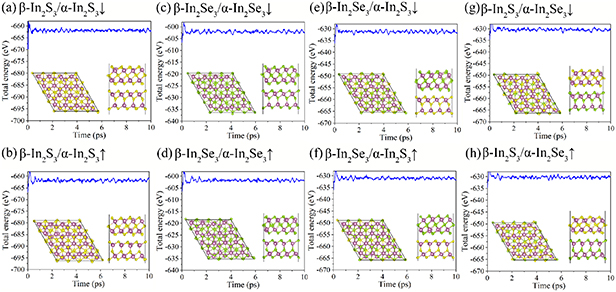
Figure 2. The total energy evolutions for (a) β-In2S3/α-In2S3↓, (b) β-In2S3/α-In2S3↑, (c) β-In2Se3/α-In2Se3↓, (d) β-In2Se3/α-In2Se3↑, (e) β-In2Se3/α-In2S3↓, (f) β-In2Se3/α-In2S3↑, (g) β-In2S3/α-In2Se3↓ and (h) β-In2S3/α-In2Se3↑ heterostructures from AIMD simulations. The inserts are the top and side views of the final structures after 10 ps simulations.
Download figure:
Standard image High-resolution imageTo reach insights into the electronic structures of the β-In2X3/α-In2X3 vdW heterostructures, the projected HSE06 band structures showing the contributions from individual layers are represented in figure 3. As described in figures 3(a), (c), (e) and (g), all the β-In2X3/α-In2X3↓ vdW heterostructures preserve the indirect band gap characteristic. Additionally, except for β-In2S3/α-In2Se3↓ heterostructure exhibit type-II band alignment feature, the others belong to type-I heterostructures. This is attributed to the fact that the conduction band minimum (CBM) and valence band maximum (VBM) of β-In2S3/α-In2S3↓, β-In2Se3/α-In2Se3↓, and β-In2Se3/α-In2S3↓ heterostructures are contributed by the β-In2X3 layer. Whereas in β-In2S3/α-In2Se3↓ heterostructure, CBM and VBM are from the β-In2S3 and α-In2Se3 layers, respectively. The calculated band gap of β-In2S3/α-In2S3↓, β-In2Se3/α-In2Se3↓, β-In2Se3/α-In2S3↓, and β-In2S3/α-In2Se3↓ heterostructures are 1.87, 1.12, 1.04 and 1.26 eV, respectively. It is worth noting that the type-II band alignment nature and suitable band gap of β-In2S3/α-In2Se3↓ heterostructure indicate its great application potential in photovoltaic devices [73]. On the other hand, for the β-In2X3/α-In2X3↑ vdW heterostructures shown in figures 3(b), (d), (f) and (h), it is interestingly seen that all of them are type-II heterostructures, as the CBM and VBM are contributed by the β-In2X3 and α-In2X3 layer, respectively. Compared with type-I heterostructures, spatial separation of carriers in type-II heterostructures effectively extends the recombination time of photogenerated carriers, which is more beneficial for the application in optoelectronic and photovoltaic fields [74–76]. Moreover, owing to the formation of type-II band alignment tailoring the band gap [29], the band gaps of the β-In2X3/α-In2X3↑ vdW heterostructures ranging from 0.55 to 0.78 eV are smaller than the β-In2X3/α-In2X3↓ vdW heterostructures.
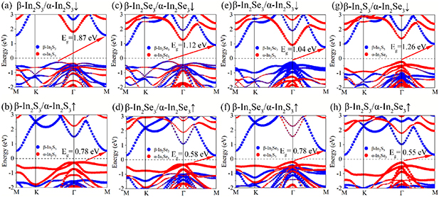
Figure 3. The project band structures of (a) β-In2S3/α-In2S3↓, (b) β-In2S3/α-In2S3↑, (c) β-In2Se3/α-In2Se3↓, (d) β-In2Se3/α-In2Se3↑, (e) β-In2Se3/α-In2S3↓, (f) β-In2Se3/α-In2S3↑, (g) β-In2S3/α-In2Se3↓ and (h) β-In2S3/α-In2Se3↑ heterostructures.
Download figure:
Standard image High-resolution imageTo unravel the physical origin of how the out-of-plane polarization of α-In2X3 monolayers modulates the band edge alignments, figure 4(a) illustrates a schematic diagram of the band energy levels in the β-In2X3/α-In2X3 vdW heterostructures. It is worth noting that the emergence of electrostatic potential differences (Δϕ) between the two surfaces of α-In2X3 leads to different band alignments of the energy bands with respect to the vacuum levels on the different surfaces. Herein, the calculated Δϕ is 1.27 and 1.18 eV for α-In2S3 and α-In2Se3 monolayers, respectively, which agree well with previous studies [33, 35]. The significant Δϕ of α-In2X3 monolayers give an excellent opportunity to achieve different types of band alignment in α-In2X3-based heterostructures as the surface of the α-In2Se3 layers in contact with the β-In2X3 layers altered with the polarization reversal [46]. Here, β-In2Se3/α-In2S3 heterostructure is proposed as an example to explain the band edge alignments modulated mechanism. The band edge alignments of β-In2Se3/α-In2S3 heterostructure before and after connecting are plotted in figures 4(b) and (c), respectively. One can see that the CBM of β-In2Se3 monolayer is 0.17 eV lower than the α-In2S3↓ monolayer, while the corresponding VBM is 0.80 eV higher. Therefore, a type-I band edge alignment is obtained after connecting β-In2Se3 and α-In2S3 monolayers to form β-In2Se3/α-In2S3↓ heterostructure. On the other hand, both the CBM and VBM energy levels of β-In2Se3 monolayer are lower than those of α-In2S3↑ monolayer, therefore, the forming of β-In2Se3/α-In2S3↑ heterostructure reaches a type-II band edge alignment. This phenomenon can be understood as when β-In2X3 monolayers are connected to α-In2X3 monolayers to form a β-In2X3/α-In2X3 vdW heterostructure, the energy bands of the two components can essentially be considered by aligning with respect to the vacuum level, owing to the nature of weak vdW interlayer interactions. Therefore, it is possible to reverse the polarization direction of the α-In2X3 layers by applying an external electric field. Hence, the attached β-In2X3 layers can contact different surfaces of the α-In2X3 layers, leading to very different band alignments of β-In2X3/α-In2X3 vdW heterostructures and even altering the type of heterostructure. Consequently, the electronic structures and optical properties of β-In2X3/α-In2X3 vdW heterostructures are changed.
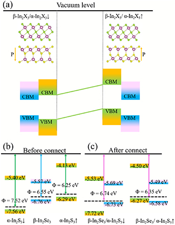
Figure 4. (a) The schematic diagram of out-of-plane polarization of α-In2X3 layers modulated band edge alignment of the β-In2X3/α-In2X3 vdW heterostructures. The band edge alignments of (b) isolated β-In2Se3 and α-In2S3 monolayers and (c) β-In2Se3/α-In2S3 heterostructures.
Download figure:
Standard image High-resolution imageThe optical absorption coefficient α (ω) of β-In2X3/α-In2X3 vdW heterostructures is one of the most critical parameters for their use in photovoltaic and optoelectronic devices, which can be calculated by [77]:
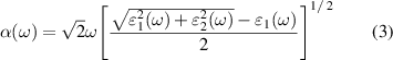
where  and
and  are the real part and imaginary part of the dielectric functions, respectively. Except for the optical absorption coefficients, the other optical properties of β-In2X3/α-In2X3 vdW heterostructures were also investigated, such as refraction indexes n (ω), extinction coefficients k (ω) reflectivities R (ω) and energy loss functions L (ω), which can be calculated as follows [77]:
Figures 5(a) and (b) show the optical absorption coefficients α (ω), refraction indexes n (ω), reflectivities R (ω), extinction coefficients k (ω) and energy loss functions L (ω) for β-In2X3/α-In2X3↓ and β-In2X3/α-In2X3↑ vdW heterostructures, respectively. Obviously, the optical absorption coefficients of the β-In2X3/α-In2X3↓ heterostructures have improved in the visible and ultraviolet light regions compared to the corresponding monolayers. Especially, the optical absorption coefficients of β-In2Se3/α-In2Se3↓ and β-In2S3/α-In2Se3↓ heterostructures are higher than the corresponding monolayers in nearly the entire visible and ultraviolet light regions. However, except for β-In2S3/α-In2S3↑ heterostructure, the increase of the optical absorption coefficients of the β-In2X3/α-In2X3↑ heterostructures is not as significant as the β-In2X3/α-In2X3↓ heterostructures, which is only enhanced in very narrow photon energy ranges. Furthermore, the refraction indexes of the β-In2X3/α-In2X3 vdW heterostructures were also evaluated. From figure 5, it can be observed that the refraction indexes of the β-In2X3/α-In2X3 vdW heterostructures are higher than the corresponding monolayers in all the spectral regions we investigated, and the values of refraction indexes following n (β-In2Se3/α-In2Se3) > n (β-In2Se3/α-In2S3) > n (β-In2S3/α-In2Se3) > n (β-In2S3/α-In2S3). Interestingly, the same trend as the refractive index can also be found in the reflectivities of β-In2X3/α-In2X3 vdW heterostructures and slightly increase with the increasing incident photon intensity. The extinction coefficient describes the degree of a given material absorbs or reflects light at a specific wavelength. Therefore, it exhibits a similar tendency to the optical absorption coefficients. In addition, it can also be found that the energy loss functions of β-In2X3/α-In2X3 vdW heterostructures are lower than the corresponding monolayer, which are beneficial to their solar cell related applications as well. Overall, the enhancement of the optical properties of the β-In2X3/α-In2X3 vdW heterostructures is conducive to its application in photovoltaic and optoelectronic devices.
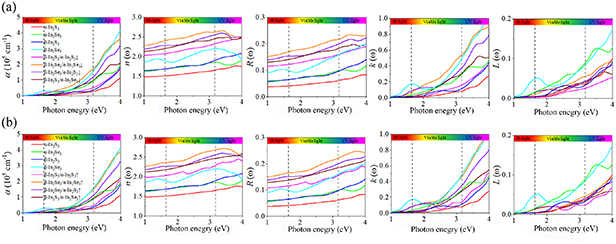
Figure 5. The optical absorption coefficients α (ω), refraction indexes n (ω), reflectivities R (ω), extinction coefficients k (ω) and energy loss functions L (ω) for (a) β-In2X3/α-In2X3↓ and (b) β-In2X3/α-In2X3↑ vdW heterostructures.
Download figure:
Standard image High-resolution imageIt is noted that β-In2S3/α-In2Se3↓ heterostructure possesses type-II band alignment with a suitable band gap, favorable optical absorption, and relatively small band offset, indicating its great potential application in the heterostructure solar cells. Therefore, to evaluate the performance of β-In2S3/α-In2Se3↓ heterostructure in solar cells, the power conversion efficiencies (PCE) η was calculated based on the following equation [78, 79]:
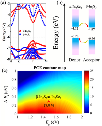
where the fill factor (βFF) is set to 0.65, VOC, JSC, Psolar, Eg and ΔEc represent the open-circuit voltage, short circuit current, total incident solar energy, band gap of donor and conduction band offset, respectively. Figure 6(a) shows the band structures of β-In2S3 and α-In2Se3 monolayers with respect to vacuum levels, which are calculated by fixing β-In2S3 and α-In2Se3 monolayers in the lattice of β-In2S3/α-In2Se3↓ heterostructure. The schematic diagram of the band edge alignment of β-In2S3/α-In2Se3↓ heterostructure is described in figure 6(b). It can be observed that the β-In2S3 and α-In2Se3 layers play as the acceptor and donor in heterostructure solar cell, respectively. Moreover, the band gap of the α-In2Se3 layer and band offset between the two layers are 1.49 eV and 0.35 eV, respectively. Based on the given parameters, a contour map depicting the relationship between Eg, ΔEc and PCE is presented in figure 6(c). The calculated PCE of the β-In2S3/α-In2Se3↓ heterostructure can be achieved at 17.9%, which is at the same level as other promising heterostructures solar cells, such as ZrS3/HfS3 (16%–18%) [80], In2SSe2/In2SeS2 (15.5%) [81], and SnS/GaSe (18%) [82], and is higher than ZrS3/MoS2 (14.2%) [83], GaTe/InS (11%) [21], and BP/SnSe (11.96%) [84].
Figure 6. (a) The band structures of β-In2S3 and α-In2Se3 monolayers fixed in the lattice of β-In2S3/α-In2Se3↓ heterostructure. (b) The schematic band edge alignments of β-In2S3/α-In2Se3↓ heterostructure in the form of individual monolayers. (c) The contour map of power conversion efficiency as a function of donor gap Eg and conduction band offset ΔEc.
Download figure:
Standard image High-resolution image
4. Conclusion
In summary, four types of the β-In2X3/α-In2X3 (X = S and Se) vdW heterostructures have been constructed, and each type of heterostructure has two different stacking configurations due to connecting of β-In2X3 monolayer to the different polarization direction of the α-In2X3 monolayer, namely the β-In2X3/α-In2X3↓, and β-In2X3/α-In2X3↑ vdW heterostructures. Their electronic structures, band edge alignments, and optical absorption coefficients have been systematically studied using DFT calculations. All the β-In2X3/α-In2X3 vdW heterostructures belong to indirect band gap semiconductors. The band alignment of β-In2S3/α-In2S3, β-In2Se3/α-In2Se3, and β-In2Se3/α-In2S3 heterostructures can be transferred from type-I to type-II by switching the out-of-plane polarization direction of α-In2X3 layers. Moreover, the optical absorption coefficients can be significantly enhanced by constructing the β-In2X3/α-In2X3 vdW heterostructures. Meanwhile, the PCE of β-In2S3/α-In2Se3↓ heterostructure can reach up to 17.9%. These results not only demonstrate the out-of-plane polarization α-In2X3 monolayers can efficiently modulate the electronic structures of the α-In2X3-based vdW heterostructures, but also provide the theoretical insight for the application of the β-In2X3/α-In2X3 vdW heterostructures in the field of optoelectronic devices and heterostructure solar cells.
Acknowledgments
This work was supported by the National Key Research and Development Program of China (No. 2022YFB3807200), the National Natural Science Foundation of China (No. 21973012), the Natural Science Foundation of Fujian Province (Nos. 2021J06011, 2020J01351, 2020J01474, 2021J01590 and 2021H6011), the Open Foundation of Key Laboratory of Green Perovskites Application of Fujian Province Universities (No. JXKFB202203), and the 'Qishan Scholar' Scientific Research Project of Fuzhou University.
Data availability statement
All data that support the findings of this study are included within the article (and any supplementary files).
Conflict of interest
The authors declare that they do not have any commercial or associative interest that represents a conflict of interest in connection with the work submitted.
Supplementary data (0.6 MB DOCX)