


Abstract
The simultaneous control of the number and position of negatively charged nitrogen-vacancy (NV) centers in diamond was achieved. While single near-surface NV centers are known to exhibit outstanding capabilities in external spin sensing, trade-off relationships among the accuracy of the number and position, and the coherence of NV centers have made the use of such engineered NV centers difficult. Namely, low-energy nitrogen implantation with lithographic techniques enables the nanoscale position control but results in degradation of the creation yield and the coherence property. In this paper, we show that low-energy nitrogen ion implantation to a 12C (99.95%)-enriched homoepitaxial diamond layer using nanomask is applicable to create shallow NV centers with a sufficiently long coherence time for external spin sensing, at a high creation yield. Furthermore, the NV centers were arranged in a regular array so that 40% lattice sites contain single NV centers. The XY8-k measurements using the individual NV centers reveal that the created NV centers have depths from 2 to 12 nm, which is comparable to the stopping range of nitrogen ions implanted at 2.5 keV. We show that the position-controlled NV centers are capable of external spin sensing with a ultra-high spatial resolution.
Export citation and abstract BibTeX RIS

Original content from this work may be used under the terms of the Creative Commons Attribution 3.0 licence. Any further distribution of this work must maintain attribution to the author(s) and the title of the work, journal citation and DOI.
Introduction
Individually addressable and controllable electron spins have a variety of technological applications, including quantum information processing (QIP) and quantum sensing. One particular electronic spin that can be optically initialized/read out and coherently manipulated by a microwave is the negatively charged nitrogen-vacancy (NV) center with the spin triplet (S = 1) ground state in diamond. These properties, in addition to a long (millisecond) spin coherence time, persist at room temperature. Thus, single NV centers form an outstanding platform for solid-state QIP at room temperature. Similarly, quantum sensing applications benefit from the excellent NV center properties, which enable the high-sensitivity detection of magnetic [1–4] and electric fields [5], temperature [6], and pressure [7]. Moreover, the highly localized spin density of the NV center provides nanoscale spatial resolution [8]. A unique capability of an optically accessible single spin sensor is the nuclear magnetic resonance (NMR) spectroscopy of small numbers of external nuclear spins on a diamond surface under ambient conditions [3, 4, 9–13]. The sensing volume, however, depends strongly on the NV center depth hence, the NMR measurement requires information about the depth of individual NV centers used as the probe. The depth information as well as the spin coherence properties allow the selection of a NV center as a spin probe that provides the detection volume and sensitivity appropriate for the target sample. Furthermore, information about the horizontal position of the NV center is useful for repeatedly accessing the NV center.
The accurate positioning of engineered NV centers is of crucial importance for both QIP and quantum sensing [14]. When NV centers are incorporated into diamond during chemical vapor deposition (CVD) or high-pressure high-temperature (HPHT) growth, three-dimensional control of the NV center positions is difficult. A tool for NV center fabrication with wide-range controllability of the depth and density is nitrogen ion implantation into a high-purity substrate followed by thermal annealing. This approach has been used in QIP applications for the fabrication of quantum registers composed of dipolar-coupled NV centers with nanometer separation. Implantation of 1 MeV 15N+ ions through nanochannels (diameter ∼20 nm) in a mica mask was used to create a pair of NV centers coupled by dipole–dipole interaction [15]. High probability of fabricating dipolar-coupled NV pairs was demonstrated by 30 keV nitrogen implantation using a resist mask with a regular array of nanoapertures (diameter ∼50 nm) [16]. While the NV–NV distance was defined by the aperture diameter in those demonstrations, a high-throughput fabrication of coupled NV centers with a separation distance of 40 nm was achieved by the implantation of 15N+ through a thin gold mask with 40 nm interval nanoapertures at an acceleration energy of 10 keV [17]. Meanwhile, maskless molecular nitrogen implantation has been employed to create a NV pair with a strong coupling [18]. Efforts to improve the positioning accuracy include the implantation of N+ at 0.5–5 keV through a small hole fabricated at the apex of an atomic-force microscope tip [19] and the suggestion of using an ion trap as the ion source for implantation with subnanometer resolution [20].
Position-controlled NV centers are also required for quantum sensing applications. In particular, the NMR spectroscopy of external spins benefits from single isolated NV centers implanted near the surface. Such shallow, single NV centers, if fabricated in a form of regular array by using nanomask implantation, are extremely useful. However, it has been reported that the creation efficiency of a shallow NV center decreases with decreasing implantation energy. According to [21], the creation efficiency is 0.1% for nitrogen ion implantation at 2.5 keV. Although implanting nitrogen ions with a high fluence is expected to compensate for the low creation efficiency, it is also known that such implantation produces too many vacancies near the NV center, which degrades the coherence properties of the NV center to an extent where it is hardly usable as a spin probe. To avoid this dilemma, the implantation of nitrogen ions at a comparatively high energy (typically 10–30 keV [17, 22–24]) is effective when single NV centers are fabricated by nitrogen ion implantation through nanoapertures. The average depth of NV centers created by nitrogen implantation at 10–30 keV has been estimated to be 15–40 nm by SRIM [25] simulation. However, to use all the created NV centers as an NMR probe, surface-sensitive shallower NV centers are desired. Therefore, for the nanoscale sensing of external spins, improving the creation efficiency is critically important as well as the control of the number and position of NV centers.
In the present work, nitrogen ions are implanted into a 12C-enriched CVD diamond layer at 2.5 keV. Our CVD film has a distinctive feature that the roughness of the as-grown surface is below 1 nm [26, 27], making it suitable for electron beam (EB) lithography. The horizontal position of the NV centers is defined by a regular array of 45 nm diameter holes fabricated in a polymethyl methacrylate (PMMA) resist film by EB lithography. The average depth, projected range, and transverse straggle for the nitrogen ion implantation into diamond at 2.5 keV are estimated to be 4.5, 1.9, and 1.6 nm, respectively, by SRIM simulation. Thus, the nitrogen implantation through the 45 nm diameter holes enables the NV centers to be localized at each lattice site of the regular array with high precision. The depth of the created NV centers was determined by detecting 1H NMR signals from immersion oil placed on the diamond surface. The depth calibration also demonstrates that the coherence properties of the fabricated NV centers can be used as probes for external nuclear spin sensing.
Methods
A 99.95% 12C-enriched homoepitaxial diamond film with a thickness of approximately 20 μm was grown on a (100)-oriented type-Ib HPHT crystal (5 × 5 × 1 mm3) by microwave plasma-assisted CVD. The conditions used for the growth of the high-quality homoepitaxial diamond film are given elsewhere in detail [27]. After cleaning in a mixture of sulfuric acid and nitric acid (3:1) at 200 °C for 30 min, the diamond surface was exposed to a remote hydrogen plasma at ∼640 °C for 5 min [28]. This hydrogen-termination treatment provides an electroconductive surface that prevents electrostatic charging upon EB irradiation. The diamond surface was coated with an EB-sensitive PMMA resist film (Microchem, 950PMMA A4) of approximately 200 nm thickness using a spin-coater. Regular arrays of 45 nm diameter holes (interval, 4 μm; grid area, 100 × 100 μm2) were patterned in the PMMA film by EB lithography. The relationship between the EB dose and the hole diameter is shown in SI figure 2 is available online at stacks.iop.org/NJP/20/083029/mmedia. To help with localization, alphanumeric characters of ∼10 μm size were also patterned. The alphanumeric pattern allows a high nitrogen dose, resulting in bright address markers consisting of NV centers located at the same depth as the regular array of NV centers, as shown in SI figure 4. After the EB lithography, nitrogen ions with a fluence of 1 × 1012 cm−2 were implanted at 2.5 keV at a tilt angle of approximately 3° from the [100] axis. Then, the PMMA resist film was removed by sonication in tetrahydrofuran, acetone, and water in that order. The diamond substrate was cleaned in a mixture of sulfuric acid and nitric acid (3:1) at 200 °C for 30 min to remove the contaminants completely. After rinsing in ultra-pure water and subsequently drying in air, the diamond substrate was annealed at 1000 °C in 10% H2 forming gas for 2 h to create NV centers. The diamond substrate was cleaned again in a mixture of sulfuric acid and nitric acid (3:1) at 200 °C for 30 min to obtain an oxygen-terminated surface. Finally, the diamond substrate was rinsed in ultra-pure water and subsequently dried in air. Photoluminescence (PL) and pulsed optically detected magnetic resonance (ODMR) measurements were performed using a laboratory-built scanning confocal fluorescence microscopy (CFM) system with 532 nm laser excitation. After soldering a Cu wire to provide microwave radiation, the diamond surface was exposed to ozone to remove the contamination caused by the Cu wiring.
Results and discussion
As shown in figure 1(a), the regular array of fluorescence spots and the alphanumeric characters can be clearly observed in the CFM image. With a few exceptions, fluorescence spots are observed only at the lattice sites of the regular array. The fluorescence spots exhibited PL spectra characteristic of negatively charged NV centers, as shown in figure 1(b). The number of NV centers per spot η was measured by the following method. Firstly, as shown in figure 1(c), photon autocorrelation measurements were performed to select fluorescence spots containing a single NV center. Namely, we selected fluorescence spots satisfying g2(0) < 0.5, where g2(τ) is the second-order autocorrelation function. Then, η was estimated from the ratio of the photon count rate of a fluorescence spot to that of a single NV center by assuming that the fluorescence intensity of a spot is proportional to the number of NV centers. Secondly, the number of NV centers in a spot was also verified from its ODMR spectrum. As shown in figure 1(d), NV centers with different orientations can be distinguished by their Zeeman splitting even if they are observed as a single fluorescence spot. As shown in figure 1(e), η ranges from zero to six in this measurement. This is because the fluctuation in the number of nitrogen ions implanted in each lattice site and the probabilistic association of a vacancy with implanted nitrogen during thermal annealing result in the probabilistic formation of NV centers at the sites. NV centers are created in 70% of the lattice sites in the regular array while 30% of the lattice sites remain empty. As shown in figure 1(e), the distribution can be fitted with a Poisson distribution with an average λ = 1.17, indicating that nearly 40% of the lattice sites contain a single NV center. These single NV centers can be accessed in a repeatable manner by using the address markers and the grid. The average number of implanted nitrogen ions per lattice site is 16 hence, the conversion yield from an implanted nitrogen atom to a NV center is evaluated to be 7.3% (1.17/16) based on the fitting. Meanwhile, the more precise conversion yield is given by the quotient of the sum of NV centers divided by the sum of implanted ions, which is evaluated to be 7.6% (143/1888). We conjecture that the small discrepancy is due to the small number of samples. We also evaluated the creation yield of NV centers for nitrogen implantation through nanoholes with different diameters. As shown in supporting information (SI) figures 1 and 2, the nanoholes of 45–100 nm diameter exhibit a creation yield of 5.6 ± 2%, suggesting that the high creation yield originates from the high CVD film quality.

Figure 1. (a) CFM image of a regular array and the alphanumeric characters 'b55' composed of NV centers. The color bar indicates the photon count per second. The numbered circles show the NV centers employed for the XY8-k measurements. Twenty-one of the 25 employed NV centers are shown in the CFM image. (b) Representative PL spectrum obtained from a fluorescence spot at a lattice site in the regular array. (c) Representative graph obtained by photon autocorrelation measurements. The second-order autocorrelation function g2(τ) reveals that the spots correspond to single NV centers. (d) ODMR spectra obtained from a fluorescence spot containing four NV centers with four different orientations. (e) Distribution of the number of NV centers per spot. The data are compared with a Poisson distribution (λ = 1.17). The number of sampled fluorescence spots is n = 118.
Download figure:
Standard image High-resolution imageNext, we measured the NV center depth by detecting 1H NMR signals from immersion oil (Nikon Type NF, proton density ρ = 68 ± 5 nm−3) placed on the diamond surface [4]. The number of NV centers employed for the NMR measurements was 25; 21 of which are shown in figure 1. We used a dynamical decoupling technique based on the XY8-k pulse sequence which acts as a high-pass filter, to filter out low frequency noise. This suppression of the noise source prolonged the electron spin coherence time of the NV centers by an order of magnitude or more. In addition to the noise suppression, the pulse sequence serves as a narrow-bandpass filter, revealing Larmor precession of the transverse magnetization of external nuclei. Signals from these statistically polarized nuclei are detected if their precession period matches the cycle of the π-pulse train applied to the NV centers. In the measurements, a magnetic field of 432 G was applied parallel to the NV axis hence the resonance condition (νN = 1/2τ) was satisfied by the π-pulse spacing of τ = 271 ns for 1H nuclear spins. The echo decay was measured for a small time range (100 ns) around 271 ns, where the 1H signal was expected. As shown in figure 2, we evaluated the NV center depth by fitting the power spectrum in the frequency domain obtained by deconvolution of the time domain spectrum using the filter function of the dynamic decoupling sequence (see also SI figure 3) [12]. Two (NV11 and NV19) of the 25 employed NV centers did not exhibit 1H NMR signals, which are presumably located at a greater depth (d > 12 nm). The histogram of the depth for the other 23 NV centers is shown in figure 3. The comparison of the experimental results with those from SRIM and Crystal-TRIM (C-TRIM) [29] simulations shows a contribution of the channeling effect to the depth distribution. Almost 50% of the NV centers are located at a depth of 2–4 nm from the surface. As described above, the depth has been determined by the observation of NMR signals of protons in immersion oil on the diamond. Thus, the single NV centers have coherence properties sufficient for using as a probe for detecting NMR signals from nanoscale volume in the sample placed on the diamond surface. The detection volume depends on the depth of the single NV center used. The depth-calibrated NV centers in a regular array with the address marker are advantageous in providing easy access to one with a desired depth repeatedly.

Figure 2. 1H NMR signals from the immersion oil placed on the diamond surface shown in the frequency domain. The applied static magnetic field is 432 G. The depths of the four NV centers are estimated to be (a) 2.84 ± 0.11, (b) 3.05 ± 0.15, (c) 4.11 ± 0.29, and (d) 7.26 ± 0.17 nm by XY8-k measurements. S(ω) is the power spectral density obtained from the time domain spectrum (shown in SI figure 3) by spectral decomposition; where ω = 2πν. The spectra (purple dots) are fitted with the Lorentz function (blue lines) to estimate the magnetic field fluctuation  from protons in the immersion oil to determine the NV center depth.
Download figure:
Standard image High-resolution image
Figure 3. Histogram of the depth of NV centers compared with the results from SRIM and CTRIM simulations. In the SRIM simulation, diamond is assumed to be amorphous, whereas in the CTRIM simulation, the diamond crystalline structure, and hence the channeling effect, is taken into account.
Download figure:
Standard image High-resolution imageFigure 4 shows the Hahn echo decay time of 19 depth-calibrated NV centers. The coherence time decreases with decreasing depth, suggesting a depth dependence in the coupling with magnetic fluctuation noise of the environment. Figure 5(a) shows the spin coherence data as a function of total evolution time for a NV center at a depth of 7.85 nm (NV23) as a function of total evolution time by varying the pulse spacing and the pulse number of Hahn-Echo, XY8-k (k = 2 and 8) and inversion recovery. In addition, the decoupling efficiency of 4 NV centers at different depths is summarized in figure 5(b). We used the fitting function exp(−t/T2)p, where p runs from 1 through 3. The scaling factor used to extend the coherence time T2 to the number (N) of pulses in the CPMG-N or XY8-k measurements is evaluated to be 0.30–0.43, which is significantly lower than the expected limit (2/3) of a simple Lorentzian bath [30].
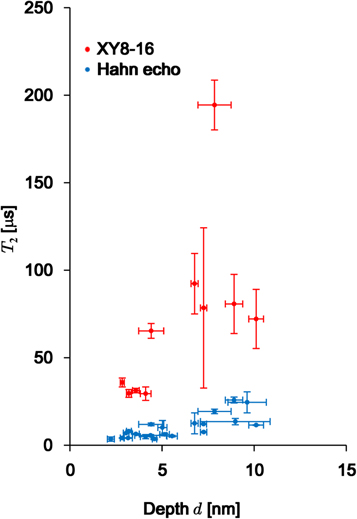
Figure 4. Relationship between the NV center depth and the Hahn echo decay time T2 (blue). The coherence time prolonged by the XY8-16 pulse sequence is also shown (red). NV center depths are evaluated by 1H NMR signals, as shown in figure 2.
Download figure:
Standard image High-resolution image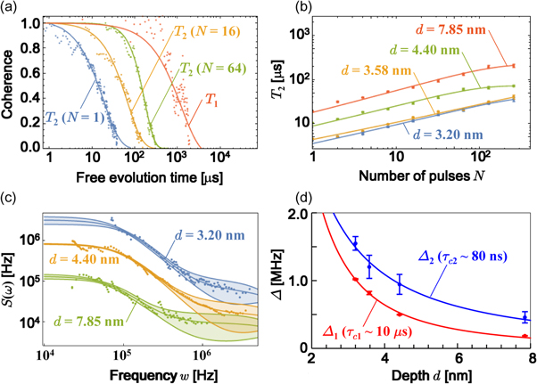
Figure 5. (a) Spin coherence data obtained by dynamical decoupling measurement as a function of total evolution time for a NV center at a depth of 7.85 nm (NV23). The line N = 1 shows the Hahn echo data, the line N = 16 shows the XY8-2 data, and the line N = 64 shows the XY8-8 data. The spin-lattice relaxation data (T1) are also shown. (b) Decoupling efficiency of four NV centers at different depths. The fitting function is exp(−t/T2)p. The lines N = 2 and N = 4 show the CPMG-N data. Other lines show the XY8-k data (N = 8k). (c) Comparison of noise spectra for NV centers at different depths. Colored regions indicate 1σ confidence regions. (d) Low- and high-frequency spin bath coupling strengths, extracted by global fitting, as a function of NV center depth.
Download figure:
Standard image High-resolution image
Implanting nitrogen ions with a fluence of 16 nitrogen ions per nanohole resulted in the formation of an average of 1.17 NV centers per spot, which enabled a high fraction (40%) of the lattice sites to be consisted of a single NV center. To determine the effect of decoherence sources on the coherence properties of the shallow NV centers, we conducted the following noise analyses. The coupling of a shallow NV center with spin bath dynamics gives rise to a noise spectrum S(ω) in the frequency domain. The coherence decay C(t) = exp[−χ(t)] in the time domain, which can be measured by periodic dynamical decoupling sequences such as Hahn echo and XY8-k sequences, is determined by the noise spectrum in the frequency domain subject to the filter function of the applied pulse sequence. The filter function acts as a bandpass filter, whose passband frequency (ω = kπ/t, where t is the total length of the decoupling sequence) dictates the region of the noise spectrum that couples with the central spin. Thus, the noise spectrum is obtained from the coherence decay curves by spectral decomposition [31]. In the noise spectroscopy of shallow NV centers created randomly by 2.5 keV broad-beam nitrogen implantation [32], the presence of two noise sources was revealed by fitting the noise spectral density S(ω) to a double Lorentzian function of the form  , where the NV—spin bath coupling strength Δi and the autocorrelation time of the spin bath τc(i) characterize the corresponding noise source. It can be determined by investigating the depth dependence
  whether the noise sources are surface-related or not. It has been reported in [33, 34] that the first term, with x1 and the correlation time τc1, originates from the two-dimensionally fluctuating spin bath of the surface electron spins. It has also been reported in [32] that the second term, with x2 and τc2, is ascribed to noise induced by the surface-modified phonons. In our sample, the noise spectra are measured for three NV centers with depths 3.20, 4.40, and 7.85 nm. The noise spectra are fitted well with a double Lorentzian function with the common correlation times τc1 and τc2 for the three NV centers at different depths, as shown in figure 5(c). The depth dependence of Δ1 yields x1 = 2.01 ± 0.06, as shown in figure 5(d), and the corresponding correlation time τc1 was evaluated to be 10 μs. This 1/d2 scaling of the coupling strength is described well by 2D surface spin bath, which is attributed to the surface electron spins [32–34]. The density of the surface electron spins (g = 2) is estimated to be ∼0.05 spins nm−2 with an average separation of 2.2 nm. The fitting of the depth dependence of Δ2 yields x2 = 1.3 ± 0.16, as shown in figure 5(d) with a correlation time τc2 of 80 ns. Note that the depth dependence of the NV—spin bath coupling strength (xi and ai) and the depth-independent autocorrelation times of the spin bath (τc1 and τc2) of the NV centers created by nanohole implantation in the present work are similar for those of shallow NV centers created by broad-beam implantation, which has been reported in [32] (table 1). Thus, the shallow NV centers created by nanohole implantation, in which an average of 16 nitrogen ions were implanted within an area of 45 nm in the diameter, do not include a significant contribution from extra noise source(s). Thus, the positioning of single shallow NV centers in a regular array has been achieved, with the NV centers having similar coherence properties to those reported for NV centers randomly positioned by broad-beam implantation [32].
Table 1. Comparison of the fitting parameters used in the noise analysis.
| Parameter | Nanohole impla. (This work) | Broad-beam impla. [32] |
|---|---|---|
| x1 | 2.01 | 1.75 |
| τc1 | 10 μs | 11 μs |
| a1 | 11.5 | 7.7 |
| x2 | 1.3 | 0.9 |
| τc2 | 80 ns | 146 ns |
| a2 | 5.6 | 2.2 |
| T2 (Hahn echo) | 3.5–26 μs | 7–51 μs |
In the present work, the Hahn echo coherence time has not been gained by the 12C enrichment since the Hahn echo decay is dominated by the contributions from the surface electron spins and the surface-modified phonons. However, it should be noted that the 12C enrichment is effective to eliminate the electron spin echo envelope modulation by 13C [12]. Moreover, the absence of the signals from the internal 13C nuclei is important in detecting those from external 13C nuclei since the signal from external 13C nuclei provides the deterministic information of the chemical structure of organic and biomolecules.
Conclusion
Using a regular array of nanoholes together with address markers patterned in a PMMA resist film by EB lithography, the positions of NV centers were well defined. Except for a small fraction of deeper centers, the fabricated NV centers have coherence properties that can be used for detecting external nuclear spins. The 1H-NMR signals from immersion oil placed on the diamond surface were detected using the NV centers, and the depths of the individual NV centers were determined. Note that a set of addressable NV centers with depths ranging from 2 to 12 nm were fabricated, and their positions and coherence properties were known. Thus, we can select a NV center appropriate for external spin sensing among the centers.
It has been reported that the thermal oxidation at 465 °C [10, 35–37] and soft oxygen plasma treatment [38] improve the coherence properties of shallow NV centers. When using these methods, the diamond surface is slightly etched and modified so as to reduce the surface electron spins acting as a noise source. Since our noise analysis indicates that the noise source is predominantly from the surface, it is expected that these methods will also be effective for our samples by decreasing the noise spectral density in the low frequency region.
High-sensitivity NMR detection under ambient conditions opens new possibilities, such as the chemical identification of an extremely small quantity of organic molecules [39]. In the near future, advanced miniaturization processes will enable the fabrication of a diamond chip with microfluidics and nanoscale vessels with the high precision alignment of single NV centers in the vicinity of the sample solution. The recent progress of single-molecule fluorescence imaging using a regular array of small cavities [40] and cell-free protein synthesis [41] could be combined with such applications to biomolecules.
Acknowledgments
This work was supported by Japan Society of the Promotion of Science (JSPS) KAKENHI (No. 26246001, No. 26220903, No. 25289109, No. 15H03980, No. 17H02751, No. 16K14242, No. 18H03766), and by DFG, BMBF, Volkswagenstiftung, ERC, and BW Stiftung.