

Abstract
In this work, structural, optical and electrical properties of ZnO thin films grown by laser ablation of a Zn metallic target on oxygen atmosphere using the 532 nm emission of the second harmonic of a Nd:YAG laser, are studied. Different mean kinetic energies of the plasma (Ek) at fixed ion density (Np) were used as control parameters. X-ray diffraction profiles show the presence of a width (002) peak together with a peak associated with the (101) reflection. Changes in Ek affect the crystallinity of the samples. An intense PL emission in the visible range of the spectra associated with a majority intrinsic donor defects can be observed. The films showed an unusual low electrical resistivity as compared to the commonly reported values for undoped ZnO thin films.
Export citation and abstract BibTeX RIS

Original content from this work may be used under the terms of the Creative Commons Attribution 4.0 licence. Any further distribution of this work must maintain attribution to the author(s) and the title of the work, journal citation and DOI.
1. Introduction
ZnO thin films have been widely studied due to its potentials applications such as solar cells, transparent conductive oxides (TCOs), piezoelectric sensors, varistors, transistors and diodes [1, 2]. This material presents interesting properties such as high excitonic binding energy (60 meV) and a direct bandgap (Eg) of 3.37 eV at room temperature (RT) that is similar to established optoelectronic materials such as GaN [1, 3]. In the literature it has been reported, for ZnO thin films, photoluminescence (PL) emissions, at RT, in the UV range (around 377 nm) [4], in the visible range (400 to 700 nm) or in both [5]. PL emissions in the UV range are associated with band to band recombination (electrons and holes) [6]. While emissions in the visible region are associated with defect carrier concentrations: donor (zinc interstitial Zni and oxygen vacancies VO) and acceptors (Zinc vacancies VZn and oxygen interstitial Oi) [7]. However, intensities of photoluminescence emissions, are also related to other physical characteristics such as crystalline quality and microstructure [8]. On the other hand, the natural electrical conductivity in ZnO is n-type and is associated to a majority concentration of oxygen vacancies, VO, and zinc interstitials, Zni [7]. However, electrical conduction in the polycrystalline ZnO is strongly related to the motion of the electrons between grain boundaries (GB model) [9, 10]. ZnO thin films produced with high optical transparency and low electrical resistivity values can be appropriate for TCOs or thin film transistors (TFT) fabrication [1, 2].
Low cost and versatility in the manufacture of ZnO thin films have allowed the performance enhancements of several experimental procedures in deposition methods such as CVD (chemical vapor deposition) [11], RF magnetron sputtering [12] or PLD (pulsed laser deposition) [13]. PLD method allows the deposition of high-quality zinc oxide nanostructured thin films, by the ablation of ZnO targets (frequently used) or by ablation of a Zn target (necessarily under O2 atmosphere). One of the most significant differences between ZnO thin films deposited by PLD from a Zn target and ZnO targets is the thickness; deposited layers by ablating of Zn metallic targets are usually thinner [14, 15], this can be an advantage in the fabrication of nanoscale devices. Dynamics of the plasma in PLD method have been used to modify the physical properties of the deposited materials [16–18]. However, there are few studies related to the control of the plasma parameters at room temperature (RT); mean kinetic energy (Ek) and plasma density (Np), in the growth of the ZnO thin films. Deposits at room temperature can present advantages as in the fabrication of films for flexible electronics applications [19]. The crystallinity of the ZnO thin films, obtained by plasma methods, such as PLD, are related to collisions of the species contained in the plasma (ions and particles) and it is usually tuned by the use of different oxygen work pressure [8, 20, 21]. The crystallinity of the deposited films can also be modified by the use of the different photon energies of the laser. In this work, the Langmuir planar probe is used to determine of Ek and Np parameters of the Zn cations contained in the plasma that interacts with an O2 reactive atmosphere at RT. From this plasma parameter and by the use of a green wavelength (532 nm) for laser ablation, crystalline, optical and electrical properties of the deposited ZnO thin films have been studied.
2. Experimental
A metallic Zn target (99.99%) rotating at 15 rpm was ablated by the second harmonic of a Nd:YAG laser (λ = 532 nm), with a 10 Hz repetition rate and a pulse width of 5 ns. The Zn plasma was generated into O2/Ar (20/80) as a reactive atmosphere. Chamber was evacuated to a base pressure of 5 × 10⁻⁵ Torr, and during the deposits, the working pressure of 2 × 10⁻² Torr was kept. The ZnO thin films were deposited on glass substrates at RT. The target to substrate distance was 5 cm. The deposition time was 30 min for all the samples. Thin films have been deposited at different mean kinetic energies (Ek) of the plasma, this has been done by varying the incident laser energy and modifying the focusing spot size on the target. Despite Ek variations, the plasma density (Np = 1 × 1013 cm−3) was kept constant, by the use of attenuating glasses whit different thicknesses.
For plasma diagnosis, a copper probe (Langmuir planar probe) was placed parallel to the substrate and perpendicular to the direction of plasma expansion. To detect the cations contained in the plasma (Zn+) the copper probe was negatively biased and connected to a circuit formed by an electrical resistance and an oscilloscope; signals were collected as a result of a potential drop in the resistance. From the signals (time of flight curves, TOF) obtained by the oscilloscope the mean kinetic energy of the plasma (Ek) as well as plasma density (Np) was estimated according to the followings relations:[22]

where m is the ionic mass and d is the distance between target and substrate,  is the ion probe current intensity and t is the time,
  is the electron charge,
  is the plasma flow velocity and
  is the collecting area of the Cu probe.
Crystalline profiles of the samples were obtained by XRD with a Panalytical Empyrean diffractometer system. The optical properties of the films were determined by UV–vis spectroscopy in the range 300 to 1100 nm with a Thermo Genesys spectrophotometer and Photoluminescence (PL) spectroscopy from 350 to 660 nm, using a 355 nm UV solid-state laser for excitation. The thickness of the ZnO samples was measured by a surface Profilometer Dektak 150. Conductivity type, resistivity, mobility and carrier concentration, were performed by Hall effect, by a Keithley 110 power supply coupled to a Walker Scientific electromagnet system.
3. Results and discussion
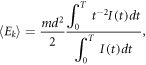
In figure 1(a) the XRD crystalline profiles normalized with the thickness (divided by the thickness) of the ZnO thin films deposited at different Ek is presented. Measurements were performed in powder diffraction mode. The diffraction pattern shows an intense peak at 36.3° corresponding with (101) plane, also a wide peak around 34.7°, corresponding with (002) plane, they belong to the Wurtzite phase of ZnO (PDF card 21-1486). The average crystallite sizes (D) were terminated with Scherrer equation [23]:

where β, λ and θ are the FWHM (full width at half maximum), x-ray wavelength and the Bragg angle of the (101) diffraction peak, respectively. The formation of a wide (002), as well as a preferred (101) orientation, are unusual for ZnO films deposited at RT. However, in the literature, S. Angappane [24], has reported the formation of preferred (101) peak at RT as well as a wide (002) peak by the use of high substrate temperatures (400 °C), in ZnO films by PLD. Apparently, the wide (002) peak could be produced by heterogeneous stress in the crystalline lattice.
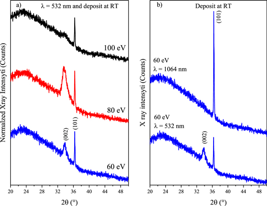
Figure 1. (a) Normalized XRD patterns at different mean kinetic energies and by ablation with 532 nm and (b) comparison of the ablation with 1064 and 532 nm in samples grown at 60 eV.
Download figure:
Standard image High-resolution imageFilms can be thought to be composed by a mixture of crystallites with (101) and (002) preferred orientations; supported by the absence of additional diffraction planes, that would appear in randomly oriented polycrystalline film. The FWHM of each peak would then correspond to the crystallite extension perpendicular to the corresponding plane, but also might include some effect from crystalline stress. The asymmetric widening observed for the (002) peak could be associated to crystallites submitted to tensile stress, inducing distortions of the crystalline lattice.
Therefore, the relative intensity (I(002)/I(101) ratio) in the XRD profile is an indicator of crystallinity in the samples, see table 1; for an intermediate Ek (80 eV) the lowest crystallinity is observed and corresponds to an 0.83 relative intensity value. However, for Ek of 100 eV balance is altered and it turns in a low intense (002) peak (I(002)/I(101) = 0.20), while, in sample grown at 60 eV the relative intensity is 0.37.
Table 1. Mean kinetic energy, crystallite size, intensity of (101), relative intensity, FWHM and band gap energy of the ZnO thin films.
| Ek (eV) | Thickness (nm) | Crystallite size from (101) plane (nm) | I(002)/I(101) (XRD counts) | FWHM From (101) | Eg (eV) |
|---|---|---|---|---|---|
| 100 | 93 | 53 | 0.20 | 0.16 | 3.36 |
| 80 | 98 | 54 | 0.83 | 0.15 | 3.35 |
| 60 | 62 | 80 | 0.37 | 0.10 | 3.31 |
Intensities of the (002) peak show a non-linear relation with Ek, meanwhile, FWHM values for the (101) peak (see table 1) have a similar value to samples grown at 80 and 100 eV (0.15 and 0.16 respectively) while the sample grown at 60 eV have a 0.10 value. FWHM values from (101) peak show correspondence whit the growth process; thickness is similar in the samples at 80 and 100 eV (93 and 98 nm respectively), but in the sample grown at 60 eV thickness is 62 nm (around 35 nm thinner). Besides, the crystallite size is around 53 nm in the samples at 80 and 100 eV while, in the sample grown at 60 eV, the crystallite size is bigger (80 nm).
The growth process is affected by increasing in Ek, reducing the reaction time of the Zn ions with the O2 atmosphere, thus, increasing the collisions between particles and ions. Both factors are compensated in samples grown at 80 and 100 eV, while in the sample at 60 eV the longer reaction time (low mobility of the ions) of the Zn+ with O2, produce (101) crystallites with an improved structural homogeneity.
For comparison purposes, a ZnO thin film grown at 60 eV was deposited using 1064 nm to ablate the Zn target and in the same experimental conditions (see figure 1(b)) than for the depositions using 532 nm. A lower crystallinity in the sample obtained by ablating with 532 nm is observed (figure 1(b)). Reduction of λ in the laser ablation process increases the amount of evaporated material from the target [18]. A proportion of this material is conformed for ionized Zn.
Crystallization of the ZnO phase is related to Zn+2 concentration in the plasma, however, in our case, the concentration of the cations in all deposits was maintained constant (Np = 1 × 1013 cm-3). Since ionization of different species than Zn+2 is unlikely, it is suggested that the use of higher photon energy generates a higher fraction of material in the plasma that is non-relevant for the formation of ZnO crystalline phase; promoting stress and inducing the formation of wide (002) peak at RT. In similar experimental conditions for ZnO by PLD (high laser energy ablation, λ = 248 nm, at RT and under O2 reactive atmosphere of 1 × 10⁻² Torr) Gupta et al [19] report the formation of a wide (110) peak. Seemly, high energy photons used to ablate under low pressure of reactive O2 can be favorable to produce this type of XRD signal.
The optical characterization in transmittance spectra was carried out in ZnO thin films and is showed in figure 2(a); an average transmittance of 85% and an absorption edge around 360 nm are found. However, transmittance from 540 nm is higher in the sample grown at 60 eV. Note that, in this sample, the absorption starts at around 27%, while in samples at 80 and 100 eV it starts at 15%. This is due to the thickness of the films, which makes evident the effect of the glass substrate in the spectrum of sample grown at 60 eV. The behavior of the curves of the figure 2(a) corresponding to samples grown at 80 and 100 eV is very similar to each other. The Optical bandgap (Eg) estimated from Tauc plots can be observed in figure 2(b) and the values are shown in table 1. Bandgap values are similar in the samples grown at 80 and 100 eV and slightly shorter in samples grown at 60 eV.
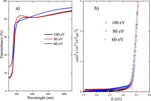
Figure 2. (a)Transmittance spectra and (b) Bandgap estimation of ZnO thin films grown at different Ek.
Download figure:
Standard image High-resolution imageEmissions in the visible range are observed for all samples deposited with 532 nm, as it is shown in figure 3(a). In the visible range, a peak around 416 nm as well as, a low-intensity band around 510 nm (figure 3(a)) are observed. However, the intensities in the samples grown at 80 and 100 eV are similar, while in the sample deposited at 60 eV is approximately 3 times higher. Changes in bandgap energy, thickness as well as in the PL intensity, show correspondence with changes in the crystallite size from the (101) crystal plane. Being, these properties, similar for samples grown at 80 and 100 eV (see table 1). Therefore, optical properties and growth process can be associated with the (101) and not with the (002) crystalline plane.
Figure 3. PL characterization for (a) films deposited by use on laser green (λ=532 nm), (b) deconvolution sample at 60 eV and (c) film deposited by use on laser IR (λ = 1064 nm) at 60 eV.
Download figure:
Standard image High-resolution image
PL emission around 405 nm (3.06 eV), observed in the deconvolution of the sample grown at 60 eV (see figure 3(b)), is related to transitions between Zn vacancies (VZn) and conduction band (CB) [23]. Emissions close to 405 nm as 393–396 nm (~3.16 eV) are associated with the electrons transition from near-band-edge (NBE) to the valence band [25]. Emissions around 423 and 444 nm (2.93 and 2.78 eV, respectively) can be associated with transitions between Zn interstitial (Zni) and the valence band (VB) [25, 26]. Also, emission around 511 nm (2.4 eV) can be associated with transitions between oxygen antisite (OZn) and VB [26]. Intensities shown in figure3(b), suggest a slightly larger concentration of the donors intrinsic defects (Zni), as compared to acceptors defects (VZn and OZn).
In ZnO thin film, deposited with 1064 nm, an intense UV emission (around 377 nm) can be observed, see figure 3(c), however, emissions localized in the visible range (associated with the intrinsic defects formation) are not observed anymore. This is in agreement with the appearance of stress for the samples deposited with 532 nm, which also induced the formation of intrinsic defects.
The electrical characterization (conductivity type, resistivity, mobility, and carrier concentration) of the ZnO thin films deposited with 532 nm was carried out by Hall effect measurements and is shown in table 2. ZnO films present n-type conductivity, this is in agreement with PL analysis (see figure 3(b)) where it was observed the majority formation of the Zni intrinsic defect (donor). Resistivity values are close in all samples, thus, seemingly, changes in Ek do not show a clear effect on the electrical properties. This behavior was not expected considering the significant differences in the crystallite sizes (for the (101) plane, see table 1), between sample grown at 60 eV and samples grown at 80 and 100 eV; since, for almost identical carrier concentration (6 × 1019 cm−3), the electrical resistivity values would increase for smaller crystallite sizes, from barrier energy at the boundary of the crystals [10]. Possibly, electrical resistivity values in the samples are compensated from the differences in defect concentrations; since PL characterization shows that sample grown at 60 eV have a greater defect concentration (acting as electron traps), thus, bringing the resistivity value closer to these of samples grown at 100 and 80 eV.
Table 2. Conductivity type, resistivity, mobility and carrier concentration pf ZnO thin film deposited by laser λ = 532 nm at different Ek.
| Ek (eV) | Conductivity type | Resistivity (Ω cm) | Mobility (cm2V−1s−1) | Carrier concentration (cm−3) |
|---|---|---|---|---|
| 100 | n | 0.008 | 11.2 | 7 × 10¹⁹ |
| 80 | n | 0.006 | 17.8 | 6 × 10¹⁹ |
| 60 | n | 0.01 | 10.9 | 6 × 10¹⁹ |
ZnO thin films showed a lower electrical resistivity value compared with literature reports; 0.1 to 0.3 Ω cm, to ZnO films deposited by PLD [21, 24, 27, 28]. However electrical resistivity values are similar to those of ZnO:Cu thin films; (0.01 to 0.2 Ω cm) [28, 29]. This unusual low resistivity could be appropriate to use the films as TCOs [1, 2].
In the polycrystalline ZnO thin films, there is a strong relation between electron mobility and (002) orientation [19]. This is in agreement with the greater mobility in the sample at 80 eV, shown in table 2, that corresponds with a relative intensity (I(002)/I(101)) of 0.83 (see table 1).
4. Conclusions
Structural electrical and optical properties of ZnO thin films, deposited by ablation of a Zn target with 532 nm and varying the mean kinetic energy of the plasma (Ek) in 60, 80 and 100 eV, have been studied. High energy of the photons impinging the Zn target in a reactive O2 atmosphere, reduces the crystallinity and causes heterogeneous stress in the crystalline lattice. This suggests the formation of two zones oriented in (101) and (002) respectively.
Sample grown at 60 eV, showed a higher crystallinity, while in the samples grown at 80 and 100 eV the structural and optical properties are similar. PL emission intensities are thought to be related to (101) plane. Samples showed an n-type conductivity, with an unusual low resistivity that could be appropriate for the fabrication of TCOs materials or TFT devices. Variation in Ek does not show a clear effect on the electrical properties, however, carrier mobility can be associated with the presence of crystals oriented in (002) plane.
Acknowledgments
Authors want to thank the technical assistance of Sergio Oliva (U de G), as well as the financial support from CONACYT (Grant: CB2010-156773), Universidad de Guadalajara (pro-SNI). JAGdeL wants to thank to CONACyT for this PhD scholarship, as well as the financial support from Doctorado en Ciencia de Materiales, CUCEI (PROINPEP, UdeG).