
Abstract
Ultraviolet (UV) sensors have gained a lot of importance in the field of environmental sciences, due to their pollution monitoring applications. The current limitations of the UV sensors are their higher temperature operability resulting in high power consumption, degradation and low efficiency. Hence an attempt was made to fabricate room temperature (RT) operable, UV index sensors, using ZnO nanorods on Indium Tin Oxide (ITO) electrodes. The nano rods were grown using hydrothermal method with an optimized concentration and growth duration of 5 mM and 3 h respectively. The vertical rods with a hexagonal face, showed an aspect ratio of six, with weak quantum confinement and a strain of the order of ∼0.002. Nanorods were polycrystalline with an average crystallite size of 50 nm. The broad emission spectra were mostly seen in blue region, with transitions due to singly and doubly ionized zinc interstitials, whose concentration increased with increase in growth duration. The UV response in direct sunlight gave a sensitivity of 118, with rise time and fall time of 35 s and 65 s respectively. The experiments not only yielded reproducible results but the UV index profile for the sensor in response to sunlight, over a full day was in accordance with the profile of the standard WHO sensor. This is of great significance especially from the point of view of ozone depletion, health concerns like skin cancer and environment pollution.
Export citation and abstract BibTeX RIS
1. Introduction
Tremendous amount of research has been done to increase the efficiency of UV sensors, which are actually indispensable to research in pollution monitoring, ozone monitoring, health issues, telecommunication, industry quality control and military applications [1–3]. By definition, a good UV sensor should exhibit high sensitivity and responsivity, sharp cut off wavelength, low dark current, high quantum efficiency, low response time and high signal to noise ratio. Currently, the commercially available sensors have certain limitations like : (i) need of filters, (ii) degrading trend, (iii) low efficiency, (iv) high response time and (v) need for high voltage input for photomultiplier [4–6]. UV sensors are broadly classified into four categories namely: (i) photoconductive detectors, (ii) Schottky detectors, (iii) p–n, pin junction detectors and (iv) MSM (metal semiconductor metal). This classification is based on the material being used and construction, which affects the performance of the device [7, 8]. In fact the performance of a UV detector depends upon many factors like the choice of active material, structure of device, electrodes and the circuitry involved, which are actually interdependent also. The active material should have a suitable structure, high surface area to volume ratio (SA/vol), high thermal and chemical stabilities and high internal gain. Various materials being experimented upon, as active materials are, II-VI compounds, III-VI compounds, ZnO, SnO2, TiO2, GaN, Si, Ge and SiC [8]. Amongst these, Metal oxides like ZnO, TiO2 are readily available, easier to fabricate, possess higher durability and are more cost effective as compared to other materials like GaN or SiC [9, 10]. ZnO is a wide bang gap semiconductor with higher chemical and thermal stabilities and a high binding energy of 60 meV. The excitons in ZnO remain stable at room temperature because of its high exciton binding energy of 60 meV which is much higher than the room temperature ionization energy of 26 meV. The excitons can efficiently generate electron hole pairs which recombine directly or via trap states. In addition ZnO has high electron mobility, high dielectric constant and high intrinsic defect density (because of the empty tetrahedral structure). Defects like Zn interstitials, oxygen vacancies which create trap states in the forbidden gap, play a vital role in making ZnO a more suitable candidate for other opto electronics devices applications also. The presence of high defect density also accounts for the broad band emission in the visible region, for ZnO to be used as a more suitable candidate for an LED [11]. Keeping in view the aforementioned properties, one can comfortable conclude that ZnO is a suitable active material for UV sensors, gas sensors, laser devices, cosmetics, LEDs and photovoltaic devices too [12, 13].
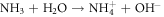
In fact, since ZnO is intrinsically an N type material and also has a high defect density, it has a high tendency to adsorb oxygen molecules on its surface which finally results into trapping of free electrons and creation of oxygen ions. This adsorption of oxygen and trapping of electrons creates a depletion layer. Hence on exposure to UV radiation, with photon energy higher than the band gap (3.37 eV) of ZnO, electron hole pairs get generated. The oxygen ions then recombine with the holes to release oxygen molecules, leading to desorption of oxygen. This is the underlying principle of ZnO UV sensors which can be expressed in the form of a chemical reaction as follows [14]:  On application of a bias, the free charge carriers flow, resulting into a change of resistance which can be taken as equivalent to the amount of UV radiation.
Keeping in view, the importance of surface area in the case of sensors, nano materials are definitely a better choice for the active material since they have a large SA/Vol ratio. That is why, with the advent of low dimensional materials, the sensitivity of sensors and other devices has improved tremendously more so because these materials possess higher mobility, quantum confinement effect and band gap modulation. In fact in 2002, after Yang and his co workers developed a single nanowire UV detector, and got a good response, research got a big boost in this direction [15, 16]. For electrodes, a lot of work has already been reported on Ag, Au, Pt, ITO, ZnO-ITO as electrode materials with various fabrication methods like MOCVD (metal-organic vapor phase deposition), PLD (pulsed laser deposition), MBE (molecular beam epitaxy) and RF sputtering [17, 18]. The electrodes need to be chosen as per its interface properties, mobility and the ease of fabrication. In the present work, ITO was chosen because of its high transparency (>95%), low cost, ready availability and its Ohmic nature of contact with ZnO. Thus Photoconductive sensors, using ZnO nanorods (NR) with ITO electrodes were fabricated using low temperature processes and incurred very low cost too. They were found to be highly sensitive, had low response times and required no amplifying device because of internal high gain. For the practical application of this sensor, its UV index profile was created in response to sunlight, over a full day. The UV index profile matched very well with the UV index profile of standard WHO sensor.
2. Experimental (material fabrication and circuit)
ZnO nanorods were fabricated on preseeded ITO coated glass substrates, by hydrothermal process [19]. ITO coated glasses which were procured from Sigma Aldrich, were cut into sixteen, 2 cm × 2 cm pieces, followed by etching of ITO in the centre, by conc. HCl. The etching was done in the center so that the ITO remaining on the sides could be used as electrodes, schematic of which s given in figure 1. This was followed by ultrasonic cleaning of cut pieces, in an ultrasonic cleaner to remove all impurities [20]. For seeding with ZnO particles, drop cast method was used wherein a 5 mM solution of Zinc Acetate dihydrate (Zn(CH3COO).2H2O ) in Ethanol was prepared, by constant stirring for an hour on a magnetic stirrer, at 60 °C. The solution turned slightly turbid after an hour. A drop of this turbid solution was poured on the substrate, which was then dried by hot air blowing at 90 °C. This process was repeated four times to get uniformly distributed zinc acetate (Zn(CH3COO) particles. To get ZnO particles, the substrates were then annealed at 350 °C for 1 h because Zn(CH3COO) decomposes into ZnO and H2O at that temperature. The reactions for the same are given as [21]:


Figure 1. Schematic for the complete experimentation processes.
Download figure:
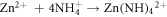
Standard image High-resolution imageTo confirm the present of ZnO particles, scanning electron microscope (SEM), X-Ray diffraction (XRD) and Photoluminescence (PL) characterizations were done on the seeded substrates. This was followed by the growth of ZnO NR by hydrothermal process. Concentrations of 5, 10, 15 and 20 mM solutions of Zn(NO3).6H2O in (de-ionized) DI water were made, by adding equal ratios of Hexamethylene Tetra amine (HMT ) and zinc nitrate hydrate Zn(NO3).6H2O in DI water and mixing the solutions separately for each concentration. A magnetic stirrer was used for mixing. The PH was checked and maintained at 6.6. The seeded glass samples were then immersed at an angle of 60°, in Teflon coated autoclaves containing the above solutions and sealed. The autoclaves were then kept at 90 °C, in pre heated furnace, for 3, 4.5, 6 and 7.5 h respectively to study the growth patterns with time. The equations involved for the growth process are given as [22]:


After the completion of growth, the sides were thoroughly washed with DI water to remove any extra salts and were systematically labeled as: XmYh where X and Y stand for concentration and growth duration respectively. Hence notation 5m3h is for sample made from 5 mM solution and annealed for 3 h and 15m7.5 h refers to a sample made from 15 mM solution grown for 7.5 h. All these 16, sensor samples were characterized for their morphological, optical and structural studies using SEM, XRD and PL. For UV response set up, the circuit used is given in figure 10 in section 3.4 of this paper. In this circuit, a high input impedance (metal oxide semiconductor (MOS)) opamp was used, since the resistance of the sensors, in dark was found to be ∼1000 M Ω. The full schematic of the procedures are given in figure 1.
3. Observation and calculations:
3.1. Scanning electron microscopy
To study the surface morphology of ZnO NR, SEM spectra were taken on the instrument JEOL-4, which are shown in figures 2, 3 and 4 for samples 5m3h, 20m3h and 20m7.5 h respectively. In figure 2, distinct vertical nanorods are seen for sample 5m3h, with an average diameter and length of 100 nm 600 nm respectively, which gives an aspect ratio 6. It was also observed that with an increase in concentration, the growth did not exhibit so much vertical nature and showed an overlapping of NR, as shown in figure 3, for sample 20m3h. The rods in this figure are not that vertical, are very dense with an average diameter and length of 100 nm 800 nm respectively giving an aspect ratio of 8. Hence one can say that with increase in concentration (from 5 mM to 20 mM), density increased because of lack of space and horizontal growth dominated the vertical growth. Further, with an increase in growth duration (from 3 h to 7.5 h), it was found that the diameter decreased, density increased even more and rods grow completely horizontally, as is shown in figure 4, for 20m7.5 h sample. The aspect ratio for these rods is 20 with average diameter of 50 nm and average length of 1000 nm respectively.

Figure 2. SEM image of 5 mM ZnO nanorods grown for 3 h (sample 5m3h). Tips show a hexagonal shape. (average diameter = 100 nm and average length = 600 nm).
Download figure:
Standard image High-resolution image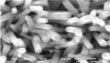
Figure 3. SEM of 20 mM ZnO nanorods grown for 3 h (sample 20m3h). Faces show a hexagonal tip and the rods are overlapping and not so vertical. (average diameter = 100 nm and average length = 800 nm).
Download figure:
Standard image High-resolution image
Figure 4. SEM of sample 20m7.5 h of ZnO nr. Rods are quite horizontal and overlapping. (Average diameter =50 nm and average length =1000 nm).
Download figure:
Standard image High-resolution image3.2. X ray diffraction
XRD spectra were taken to study the structure, particle size and strain in ZnO nr. The spectra taken were in the range of 2θ values from 20° to 70o on Bruker-DS, which are displayed in figures 5 and 6 respectively for 20m4.5 h and 15m7.5 h samples. From these spectra, it is clear that the main peaks in ZnO nr samples were at 31.8°, 34.5° and 36.2° for (100), (002) and (101) planes and at 47.5° and 56.6° for (102) and (110) planes respectively. All the peaks showed a Gaussian profile, indicating polycrystalline behavior of the ZnO NR. No other impurity peaks were found. Figure 5 shows the XRD peaks for sample 20m4.5 h, where the intensity for (101) is higher than (002) peak intensity whereas peak intensity for (002) is higher than (101) plane for sample 15m7.5 h (figure 5). In fact, 11 out of 16 samples exhibited maximum intensity in (002) direction, indicating a preferential growth in that direction. For the rest of the 5 samples, the maximum intensity was in (101) direction conforming with JCPDS (file # 043–0002) data for ZnO [23, 24]. This proves that for the nano rods growth, C plane direction was preferred over (101) plane direction, which is also evident from the SEM pictures (vertical growth with a hexagonal tip). Also no consistent change in peak intensity or position was observed due to change in annealing duration or concentration.
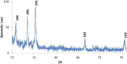
Figure 5. XRD spectra of 20m4.5 h sample of ZnO nanorods.
Download figure:
Standard image High-resolution image
Figure 6. XRD spectrum of 15m7.5 h sample of ZnO nanorods.
Download figure:
Standard image High-resolution imageTable 1 shows to a comparison between the peaks and intensities of standard ZnO (JCPDS) and the current ZnO NR samples for different concentrations. (15m3h, 20m3h, 15m4.5 h, 20m4.5 h, 10m6h, 15m6h and 15m7.5 h). In this table, columns 2 and 4 show JCPDS data where a maximum of 100 is exists for (101) plane [25]. Columns 5 to 11 give the relative intensities of present samples, where maximum intensity is in (002) for 3 samples and in (101) plane for rest of the four samples. There is a slight shift in the peak positions with respect to JCPDS data, in the present samples, which could be attributed to either instrumental error or due to different growth mechanisms.
Table 1. Table for XRD 2θ peak position with respective intensities for ZnO bulk ( JCPDS data) and for present ZnO nr samples.
| (hkl) | 2 θ | INTENSITY | ||||||||
|---|---|---|---|---|---|---|---|---|---|---|
| ⇓ | JCPDS | ZnO | JCPDS | 15m3h | 20m3h | 15m4.5 h | 20m4.5 h | 10m6h | 15m6h | 15m7.5 h |
| (100) | 31.770 | 31.8 | 57 | 67 | 66 | 66 | 70 | 67 | 43 | |
| (002) | 34.422 | 34.5 | 44 | 100 | 100 | 100 | 78 | 89 | 98 | 100 |
| (101) | 36.253 | 36.2 | 100 | 98 | 97 | 77 | 100 | 100 | 100 | 70 |
| (102) | 47.539 | 47.5 | 23 | 32 | 27 | 33 | 21 | |||
| (110) | 56.603 | 56.5 | 32 | 34 | 20 | 34 | 27 | 17 | ||
To estimate the average grain size (grain referring to the dimension of coherent diffracting domains) and strain, Williamson Hall method was used [22, 25], according to which the relation between strain, particle size and 2 θ position can be expressed as Williamson Hall equation, given by:

where βhkl is the FWHM of the XRD peak, θ is the Bragg's diffraction angle, λ is the K-Cuα wavelength (=1.54A°) of X-ray, Rhkl is the linear dimension of the diffracting domain along a direction normal to plane (hkl). For the above analysis, the peaks in (100), (002), (101), (102) and (110) planes were used. Graphs between β Cos(θ)/λ versus Sin(θ)/λ for 5m7h and 5m4h samples were drawn and linear fits were plotted, as shown in figure 7. The average particle size and strain were calculated from the y intercepts and slopes of the linear fits given by equations: y = 0.0049x + 0.0158 and y = 0.0056x + 0.0133 for 5m7h and 5m4h samples respectively.

Figure 7. Williamson-Hall plot for 5m4.5 h and 5m7.5 h ZnO nr samples showing linear.
Download figure:
Standard image High-resolution imageThe grain sizes for 5m4.5 h and 5m7.5 h samples were found to be 63 nm & 75 nm respectively. The strain values were estimated to be in the range of 0.0015 to 0.006. Table 2 lists the values of grain sizes and strains calculated for all 5 mM samples. It is clear from the table that the grain size has increased from 42 nm to 75 nm with increase in growth duration from 3 h to 7.5 h.
Table 2. Grain sizes and strains for 5 mM ZnO nr samples.
| 5m3h | 5m4.5 h | 5m6h | 5m7.5 h | |
|---|---|---|---|---|
| Grain size (nm) | 42.7 | 46 | 63 | 75 |
| Strain | 0.0015 | 0.0027 | 0.0015 | 0.006 |
3.3. Photoluminescence
To study the nature of excitonic and non excitonic emissions and the related trap phenomena for ZnO NR, PL spectra were taken at room temperature and figure 8 and figure 9 show the PL spectra for 5 mM and 20 mM samples respectively. From these spectra, it is clear that a wide band emission is present from 380 nm (3.37 eV) to 493 nm 2.55 eV), with maximum peak at 438 nm and other peaks and shoulders at 414 nm (3 eV), 438 nm (2.87 eV), 465 nm ( 2.69 eV), 470 nm (2.68 eV), 483 nm (2.60 eV) and 493 nm (2.55 eV). From amongst all the 5 mM samples (figure 8), the intensity of 438 nm peak is maximum at 700, for a growth duration of 3 h (5m3h) and only a shoulder appears at 493 nm. With increase in growth duration, the overall intensity and intensities of respective peaks decrease, as shown by four curves marked as 5m3h, 5m4.5 h, 5m6h and 5m7.5 h. It was also observed that with increase in mM concentration, the maximum peak position shifted from 438 nm to 467 nm, as shown for 20 mM samples, in figure 9. Also a comparison between the spectra of figures 8 and 9 shows that overall luminescence intensity decreases with increase in both concentration and growth duration. One can thus conclude that with increase in concentration, the emissions shifted more towards lower energy trap states.

Figure 8. PL spectra for 5 mM samples of ZnO nanorods respectively.
Download figure:
Standard image High-resolution image
Figure 9. PL spectra for 20 mM samples ZnO nanorods respectively.
Download figure:
Standard image High-resolution imageIn fact upon photo excitation of a fluorescent material, any or all of the three processes can take place, namely: (i) Excitonic emission, (ii) Trap related emission and (iii) Non radiative emission [25, 26]. In the present samples, it was observed that trap related emissions dominated over the excitonic emission, which is actually a major reason for high sensitivity of the UV sensor; in other words it is because of presence of numerous defects, that the sensitivity is so high. Also the nanorods have a large SA/vol ratio more photo generated holes get captured in trap states. For ZnO, the probable candidates for hole trapping are O2− ions at its surface [19]. This trapping is also related to the particle size in the sense that as the size increases the surface area decreases but the transition rate for exciton should not be affected by the size change. ZnO being an open structure with HCP, where Zn occupies only half the tetrahedral sites and all the octahedral sites being empty, there is maximum tendency of accommodating intrinsic defects which also accounts for the dominated defect related emissions. Upon irradiation, various transitions taking place are: (i) VB to CB and VB to shallow levels (ii) Subsequent transition from CB to deep levels and shallow levels to deep levels which gives rise to violet, blue or green emission depending upon the energy difference. The oxygen vacancies Vo+, Vo++ defects are situated approximately 2 eV below the conduction band and these trap states have been presumed to be the recombination centre for green emission in general. After such a recombination a neutral state Vox, is formed whose level is just below (∼0.8 eV) the conduction band. Besides the oxygen vacancies, more defects namely Zn interstitials, singly and doubly ionized interstitials (Zni+, Zni++) give rise to blue emission. Zni is located at 0.22 eV below the CB and is responsible for the violet emission (∼380 nm). Lower wavelength (blue) emission are supposed to occur due to deeper (0.37 eV) location of Zni. More traps due to defects of Zni+ and Zni++ are approximately 0.56 eV and 0.63 eV below the CB from where transitions may take place to VB or zinc vacancy (Vzn) thus giving blue emission again. Figure 10 gives the contributions of these defect related emissions for ZnO nr. These are only approximate since different authors have reported different states for same defects respectively [27, 28].

Figure 10. Pl spectrum of ZnO nr (20 mM samples) shown with PL peak positions and corresponding emissions as per defect related trap states, in the energy band diagram of ZnO.
Download figure:
Standard image High-resolution imageTo estimate the transition levels (quantum states) corresponding to various emissions, one can combine the 1d quantum confinement model and Williamson - hall method [29]. The crystallite size of the present ZnO NR (diameter = 30 nm) were found to be much higher than the ZnO exciton Bohr radius (=2.34 nm), because of which one can say that the quantum confinement lies in the weak regime. Hence using the weak quantum confinement regime and Williamson-Hall method, the expression for n → 1 transition can be written as [29]:
From the above equations it can be concluded that α depends upon the grain size R. Table 3 gives the values of transition levels for different PL peaks and the same data is plotted in figure 11.
Table 3. Values of transition levels (n) and emission wavelength for 40 nm particle of ZnO.
| Wavelength(nm) | 373 | 414 | 438 | 465 | 470 | 480 | 493 |
|---|---|---|---|---|---|---|---|
| Transition level (n) | 79 | 74 | 69 | 66 | 66 | 65 | 65 |
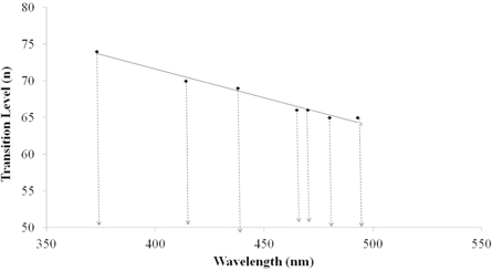
Figure 11. Plot between emission wavelengths (nm) versus transition levels (n) for 40 nm ZnO particle.
Download figure:
Standard image High-resolution image3.4. UV index sensor
For UV response and UV index measurements, 5 mM samples were selected because of their better morphological results as compared to other concentrations (section 3.1). The circuit used for sensitivity measurement is shown figure 12 where a very high impedance opamp TL074 was used. This opamp has almost infinite input impedance (MOS opamp), which is suitable for the ZnO NR sensor since the impedance of NR was estimated to be in the range of ∼1000MΩ, in dark.

Figure 12. Circuit diagram for UV light response measurement. Rd is the ZnO sensor resistance, Rin = 67MΩ and opamp TL074 is used in voltage follower configuration.
Download figure:
Standard image High-resolution imageIn this circuit, Rd is the device resistance to be measured, Vin = 8 V, Vo is the output voltage, Rin = 67 MΩ and the opamp TL074 is used in the voltage follower configuration. The sensor was kept in a black box with a shutter, which was opened and closed for UV radiation exposure (from sunlight). The sensitivity measurements were taken at roof top, every one hour, starting at 8am till 6 pm, over many days. Care was taken to avoid the days with variation in humidity or cloudiness. The output response of the four sensors (5m3h, 5m4.5 h, 5m6h and 5m7.5 h) is plotted in figure 13. In this figure, 5m3h sample showed the least rise time and fall time of 28 s and 32 s respectively, in comparison to other samples. The rise time was calculated as the time required to reach 90% from 10%, of the saturation value and fall time is the time taken to reach 10% from 90% of the saturation value. In figure 14, the rise time trends for all sensors are plotted again. Similarly figure 15 shows the fall time trends separately, for all sensors. All the rise times and fall times are also listed in table 4 along with sensitivity of four sensors.

Figure 13. UV response of four sensors made from 5 mM ZnO nanorods with growth times of 3 h (5m3h), 4.5 hrs (5m4.5 h), 6 h (5m6h) and 7.5 h(5m7.5 h) respectively.
Download figure:
Standard image High-resolution image
Figure 14. The rise time of 4 sensors (5m3h, 5m4.5 h, 5m6h & 5m7.5h) marked as 28 s, 35 s, 55 s & 77 s respectively.
Download figure:
Standard image High-resolution image
Figure 15. The fall time of 4 sensors (5m3h, 5m4.5 h, 5m6h & 5m7.5 h) marked as 37 s, 120 s, 95 s & 130 s respectively.
Download figure:
Standard image High-resolution imageTable 4. Table showing rise time and fall time of four 5 mM ZnO nr sensors.
| SN | Rise Time (sec) | Fall Time (sec) | Sensitivity |
|---|---|---|---|
| 5m3h | 35 | 46 | 118 |
| 5m4.5 h | 49 | 64 | 102 |
| 5m6h | 70 | 132 | 95 |
| 5m7.5 h | 76 | 160 | 88 |
The sample 5m3h, showed the highest sensitivity of 118 with least response times, hence this sample was chosen to create a UV index profile, where conductance was plotted against time, as shown in figure 16. In this fig, the UV index profile of the standard WHO sensor [30], is plotted on the main vertical axis whereas the secondary vertical axis show conductance profile for 5m3h sample. Both the graphs were normalized. As can be seen, with increase in radiation intensity around 13 h, the conductance increases to maximum and decreases on both sides as the Sunlight intensity decreases in the morning and evening. The matching of these two profiles proves that the 5m3h sensor sample can be easily used as the UV index device. A slight deviation which was observed could be accounted for due to difference in humidity or other conditions of the atmosphere.

Figure 16. Calibrated UV index plotted against time for 5m3h sensor shown by solid curve. Dotted curve is the WHO standard UV index.
Download figure:
Standard image High-resolution image
4. Conclusions and results
UV index sensors were fabricated using ZnO nanorods and ITO electrodes. The nanorods grown from 5 mM concentration and with a growth duration of 3 h, gave the best morphological results in comparison with other concentration and growth durations. The SEM results proved that the NR for 5m3h sample, were vertical whereas the NR in other samples of higher concentrations and growth durations, (>5 mM) were not so vertical overlapping arrays. The diameter and length were 100 nm and 600 nm respectively for 5m3h ZnO sample, giving an aspect ratio of 6. The material was polycrystalline in nature as shown by the Gaussian peaks of XRD spectra with an increase in average grain from 42 nm to 75 nm with an increase in annealing duration from 3 h to 7.5 h. Also 11 out of our 16 samples showed a preferential growth in (002) direction instead of (101) plane unlike that for bulk ZnO, with slight variation in 2θ peak positions which could be lattice strain. The NR exhibited weak quantum confinement since particle size was much higher than the Bohr's exciton radius for ZnO. The transition levels were estimated to be from levels 65 to 79 to level 1. PL spectra showed a broad emission spectrum from 380 nm to 493 nm with peaks and shoulders at 413 nm, 453 nm, 440 nm, 467 nm, 483 nm & 493 nm. These were mostly due to Zn interstitials and Zn++ ionized vacancies. The maximum PL intensity of 770 was observed at 413 nm for 5m3h sample, which decreased both with increase in concentration and growth duration. With increase in growth duration, the 440 nm (2.86 eV) peak showed higher intensity than 413 nm (3.06 eV) peak suggesting that the density of ionized Zn defects increased with time. UV sensitivity was measured in direct sunlight under normal humidity conditions. The rise time and fall time of 5m3h sensor was estimated to be 35 s and 46 s respectively with a sensitivity of 118. The UV index profile of our 5m3h low cost sensor, matched very well with the UV index profile of WHO standard sensor. Thus this 5m3h sensor can be used as a non degrading, sturdy UV index sensor.
Acknowledgments
The authors wish to acknowledge and thank the University of Delhi for its financial support to buy material and equipment for this work under the Innovation project RD202. We also thank Mr Harsh, University Science Instrumentation centre for allowing the conduction of PL, SEM and XRD studies. We also extend heartfelt gratitude to the Principal, Rajdhani College for support to conduct this work. Students Brijesh and Manish contributed significantly in experimental and theoretical procedures and hence heartfelt thanks to them also.