
Abstract
We studied the electrical properties of polysilicon/hafnium (Hf)-silicate gate stacks with various controlled  compositions, using bis-dimethylamino-silane (BDMAS:
  ) and tris-dimethylamino-silane (TDMAS:
  ) as precursors. The high-
 films were fabricated by atomic layer deposition (ALD) using
  and each of the Si precursors in turn.
  was used as an oxidant. Effective oxide thicknesses (EOTs) were reduced in line with increasing Hf contents: the very thin dielectric
  was fabricated with a
  composition of 74%. The flatband voltage
  shift of p-type metal oxide semiconductor field effect transistors (p-MOSFETs) employing either Si precursor were improved by reducing the
  composition: the value of
  shift was improved to about
  for Hf-silicate gate stacks in which
  composition was reduced from 72–74% to 21–23%. The subthreshold swings (S values) were dependent on the Hf content in the p-MOSFETs employing both Si precursors. By using the gate length (Lg) of the transistors as
  ,
,  values varied from
  /dec for
  composition ratios from 21 to 74%, respectively, due to a Fermi-level pinning problem. Inspection of subthreshold characteristics of n-MOSFETs revealed values of
  at
at  , which were greater than
  , while
  was less than
  , using either Si precursor
  . With the p-MOSFETs, the values of
  at
at  for Hf-silicate gate stacks in which
  composition was between 21 and 23% were approximately
  greater than those in which
  composition was between 72 and 74%. The leakage current densities were dependent on the Hf content in the Hf-silicate gate stacks. However, those were independent of the Si precursors for the Hf-silicate gate stacks with the same Hf content, because the carbon impurity concentrations near the surface of the annealed layers at
  were about
  for both Si precursors.
Export citation and abstract BibTeX RIS
For many years, silicon dioxide  films have been the gate dielectric in complementary metal oxide semiconductor (CMOS) devices. For gate oxide thicknesses of less than
  , the direct tunneling current increases by a factor of 100 times for each
  decrease in thickness.1, 2 This high gate leakage current increases the standby power consumption.2 In order to reduce the leakage current due to direct tunneling, high-dielectric-constant (high-
 ) materials allow for an increase in the physical thickness while maintaining a low equivalent oxide thickness.3–8 Among the many high-
 materials available, those based on Hf and its nitride exhibit low leakage currents and high carrier mobility.7, 8
Sputtering and metallorganic chemical vapor deposition (MOCVD) are two methods that have been used for the formation of high- films.3–8 Another possible deposition technique is atomic layer deposition (ALD), which has some desirable features in that it allows precise control of composition, film thickness, conformality, and uniformity.9–15 Hafnium-tetrachloride
  and water
  have been widely used to deposit
  using the ALD technique.9, 10 There have been reports of groups using Hf amide-type precursors such as
  for growing
  or Hf-aluminate films in order to solve the problem of particles that occurs when using
  precursors.11–16 Furthermore,
  and
and  precursors are interesting materials because their melting points are very low (less than
  ) and they exhibit high vapor pressures (92 and
  at
at  , respectively).15, 16 It has been reported that the thickness and
  composition ratios of ALD Hf-silicate films could be easily controlled by regulating the number of deposition cycles using
  and TDMAS
  , or
, or  and BDMAS
  precursors.15, 16 The flatband/threshold voltage
  of poly-Si gated p-type metal oxide semiconductor field effect transistor (p-MOSFETs) formed using Hf-based gate dielectrics is unacceptably high due to Fermi-level pinning.17 Recently, the suppression of these shifts in
  has been studied for Si-rich Hf-silicate gate dielectrics
  in poly-Si gated p-MOSFETs.17–20
In this study, we investigated the effect of  composition on the electrical properties of poly-Si gated n- and p-MOSFETs, incorporating ALD Hf-silicate gate dielectrics that had been fabricated using
  and TDMAS, or
  and BDMAS precursors.
Experimental
The substrates that we used were  p-type Si(100) wafers. Immediately following a pretreatment with diluted (0.5%) HF, a
  -thick SiON layer was formed by rapid thermal processing (RTP) in an NO ambient at
  for
for  to prevent boron penetration and interfacial layer growth. After the underlayer formation, Hf-silicate films were deposited by using an ALD technique.
  was used to form the
  layers, and TDMAS or BDMAS were used to form the
  layers. A single ALD cycle for
  consisted of the following process: the
  precursor was introduced into the reactor chamber for
  , after which it was purged for
  . This precursor was introduced using a liquid flow meter system and vaporized at
  with Ar as a carrier gas. Following this,
  was introduced for
  as an oxidant and then purged for
  . The
. The  and the carrier gas had flow rates of
  and
and  , respectively. A single ALD cycle for
  consisted of the following process: the Si precursor was introduced into the reactor chamber for
  and was then purged for
  , and an oxidant
  was introduced for
  and purged for
  . In this ALD
  process, BDMAS was directly introduced into the reactor chamber and controlled using a mass flow system at
  , because the vapor pressure of BDMAS is very high. The BDMAS had a flow rate of
  in order to obtain good uniformity of better than 5%. TDMAS was introduced into the reactor chamber using a liquid mass flow system and vaporized at
  with Ar as a carrier gas. The TDMAS and carrier gas have flow rates of 10 and
  , respectively, to obtain good uniformity of better than 5%. In the process, a buffer gas of Ar always flowed at
  into the reactor chamber.
  was used as a source of oxygen using an
  flow ratio of
  with the concentration of
  in
in  being
being  . The pressure in the ALD reactor chamber was controlled at
  for
for  deposition, and at
  and
and  for TDMAS-
 and BDMAS-
 deposition, respectively.15, 16 The film depositions were carried out at
  . The
. The  compositions of the ALD Hf-silicate films were controlled by varying the
  ratio in the gas-phase: compositions of 23, 44, and 74% were achieved for ratios of
  ,
,  , and
, and  for TDMAS; and 21, 48, and 72% were achieved for ratios of
  ,
,  , and
, and  for BDMAS, respectively.15, 16
In this transistor device fabrication process, counterimplantation was applied to reduce the  for p-MOSFETs after the well formation.21 The channel doping concentrations were about 5 and
  for n-MOS and p-MOSFETs, respectively. After the formation of high-
 gate stack dielectrics, the films were nitrided using a nitrogen radical plasma treatment.8 The nitrogen plasma was formed in an
  ambient at
  at
at  using a
  radio frequency (rf) power supply. After nitridation, the films were treated in an
  -diluted oxygen atmosphere (
 concentration of 0.1%) at
  for
for  as a postnitridation annealing (PNA). Polysilicon was then deposited on the high-
 gate stack to provide the gate electrodes, and boron and phosphorus were implanted as p- and n-type dopants, respectively. After patterning and etching of the polysilicon gate electrodes, rapid thermal annealing (RTA) was performed at
  for
for  to activate the dopants. The samples were then annealed at
  for
for  in forming gas (
 mixture).
The film thickness and uniformity of the Hf-silicate and  films were measured with an ellipsometer over
  wafers. The composition of the Hf-silicate films was measured using high-resolution Rutherford backscattering (HR-RBS) analysis with a
  helium ion
  beam. Capacitance-voltage (C-V) and current-voltage (I-V) measurements were performed in parallel on an HP 4284A LCR meter at high frequency
  and an HP 4156C parameter analyzer. The effective oxide thicknesses (EOT) and flatband voltage
  of the films were calculated using an analytical quantum mechanical model.22 The effective mobility was measured by applying a modified split C-V method. The interfacial trap density (Nit) was evaluated from the charge-pumping current (Icp) at room temperature.14 Residual impurities such as carbon and hydrogen were analyzed by secondary ion mass spectrometry (SIMS) with a
  cesium primary ion
  beam. The primary ion beam was raster scanned over an area of
  .
.
Results and Discussion
Figure 1 shows the C-V characteristics of ALD Hf-silicate gate stacks employing TDMAS for (a) n-MOSFETs and (b) p-MOSFETs. Hf-silicate films were evaluated with three different Hf contents (Hf 74% using  , Hf 44% using
  , and Hf 23% using
  ratio). As shown in Fig. 1, the EOTs of these films were 1.18, 1.32, and
  for
for  compositions of 74, 44, and 23%, respectively, in the Hf-silicate gate stacks: the EOTs were reduced with increasing Hf contents due to increases in their dielectric constant
  . The
. The  of all of the n-MOSFETs were almost the same, however, those of the p-MOSFETs were dependent on the Hf content of the Hf-silicate gate stacks.
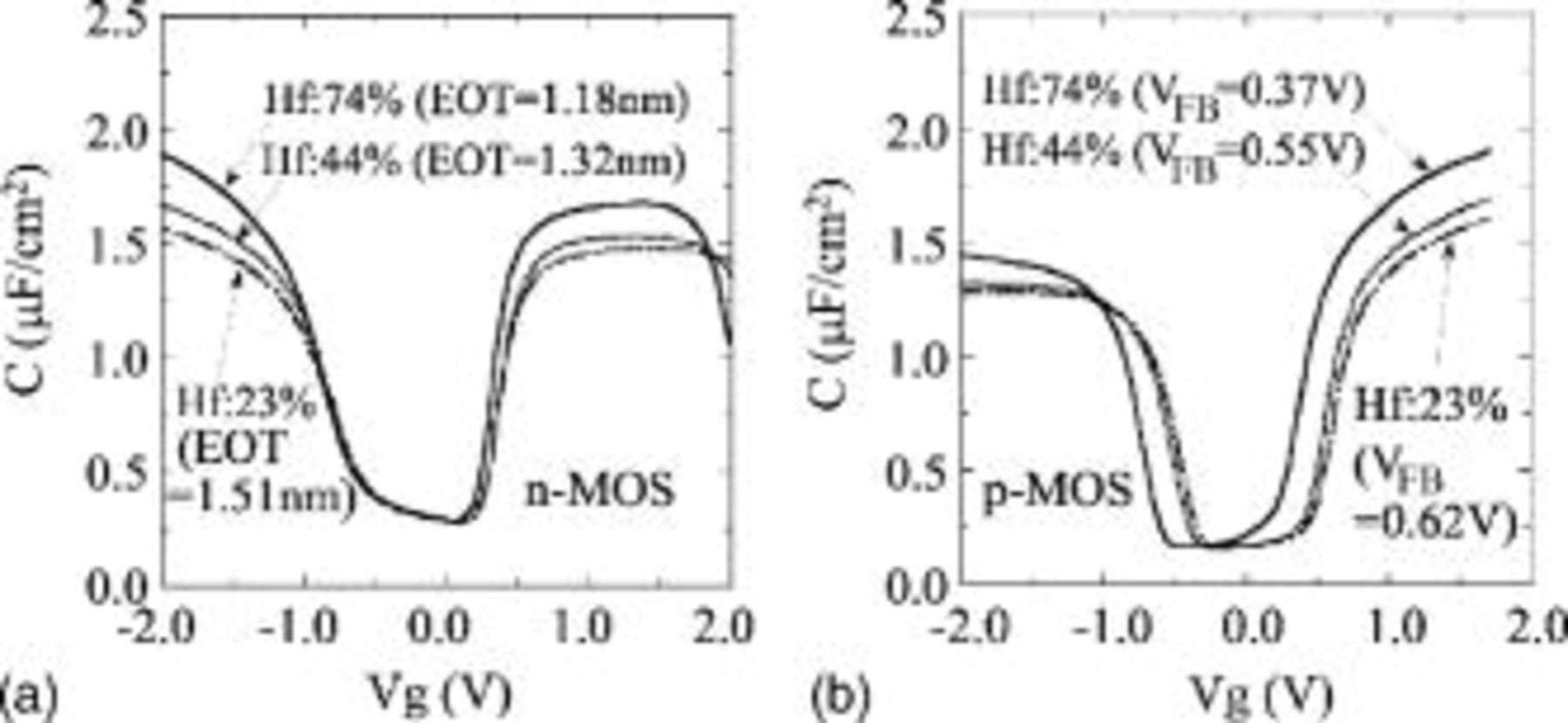
Figure 1. C-V characteristics of ALD Hf-silicate gate stacks employing TDMAS for (a) n-MOSFETs and (b) p-MOSFETs. Hf-silicate films were evaluated with three different Hf contents (Hf 74% using  , Hf 44% using
  , and Hf 23% using
  ratios). C-V measurements were performed using capacitors with an area of
 . The EOT and flatband voltage
  were calculated from the analytical quantum mechanical model.22
Figure 2 shows the C-V characteristics of ALD Hf-silicate gate stacks employing BDMAS for (a) n-MOSFETs and (b) p-MOSFETs. The Hf-silicate films possessed almost the same Hf contents as in the TDMAS case; the  compositions of 72, 48, and 21% were achieved with ratios of
  ,
,  , and
, and  , respectively. As shown in Fig. 2, the values of EOT were reduced with increasing Hf contents and the
  values of the p-MOSFETs were also dependent on the Hf contents of the Hf-silicate gate stacks.
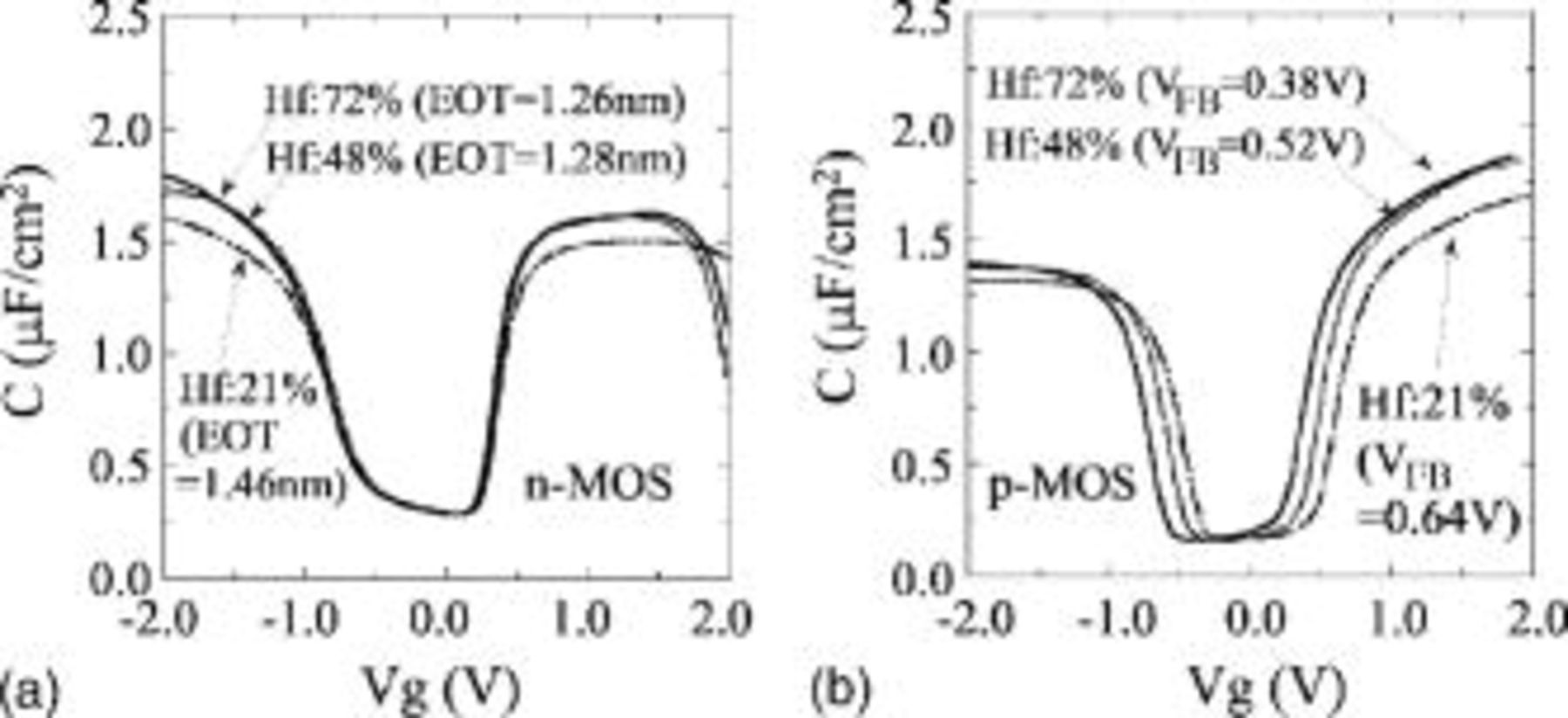
Figure 2. C-V characteristics of ALD Hf-silicate gate stacks employing BDMAS for (a) n-MOSFETs and (b) p-MOSFETs. Hf-silicate films were evaluated with three different HF contents (Hf 72% using  , Hf 48% using
  , and Hf 21% using
  ratios).
Figure 3 shows the dependence of  on the
  composition in the ALD Hf-silicate gate stacks, using TDMAS and BDMAS precursors, for n- and p-MOSFETs. As shown in Fig. 3, values of
  of n-MOSFETs were slightly increased by reducing the
  composition: the value of
  shift was about
  . Values of
  shift of p-MOSFETs were improved by reducing the
  composition: the improved value of
  shift was about
  for
for  compositions of 23–21%. Furthermore, these results were not dependent on the Si precursors. This probably occurs because the Fermi-level pinning problem is suppressed by Si-rich Hf-silicate films; however, there is still the Fermi-level pinning problem because the value of
  is about
  for the poly-
 sample using the same conditions of device fabrication process.17–20 The reason for this result is still not fully understood.
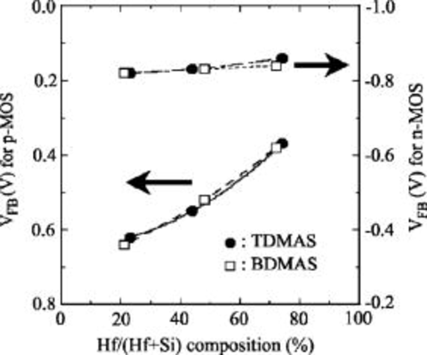
Figure 3. Dependence of  on the
  composition in the ALD Hf-silicate gate stacks, using TDMAS and BDMAS precursors, for n- and p-MOSFETs.
Figure 4 shows the subthreshold characteristics of ALD Hf-silicate gate stacks with different Hf contents using (a) TDMAS and (b) BDMAS precursors. In this measurement, the gate length (Lg) and the gate width  of the transistors used were
  and
and  , and the applied voltages between the drain and the source were 1.1 and
  for the n- and p-MOSFETs, respectively. The subthreshold swings (
 values) for all samples were good, being less than
  /dec for n-MOSFETs. The S values were dependent on the Hf content of Hf-silicate gate stacks for p-MOSFETs: these varied from
  /dec for
  compositions from 21 to 74%, respectively. The drain currents
  at
at  were less than
  in both n- and p-MOSFETs. The drain current
  at
at  in the n-MOSFETs fabricated using BDMAS were larger than those using TDMAS because the values of
  of BDMAS devices were slightly larger than those using TDMAS. The values of
  were greater than about
  . Meanwhile, the values of
  in the p-MOSFET samples were dependent on the Hf-content. The values of
  for Hf-silicate gate stacks containing
  compositions of 72–74% were about
  less than the values in devices with
  compositions of 21–23%, probably due to the Fermi-level pinning problem. The processing parameters and electrical properties of these samples are summarized in Table I.
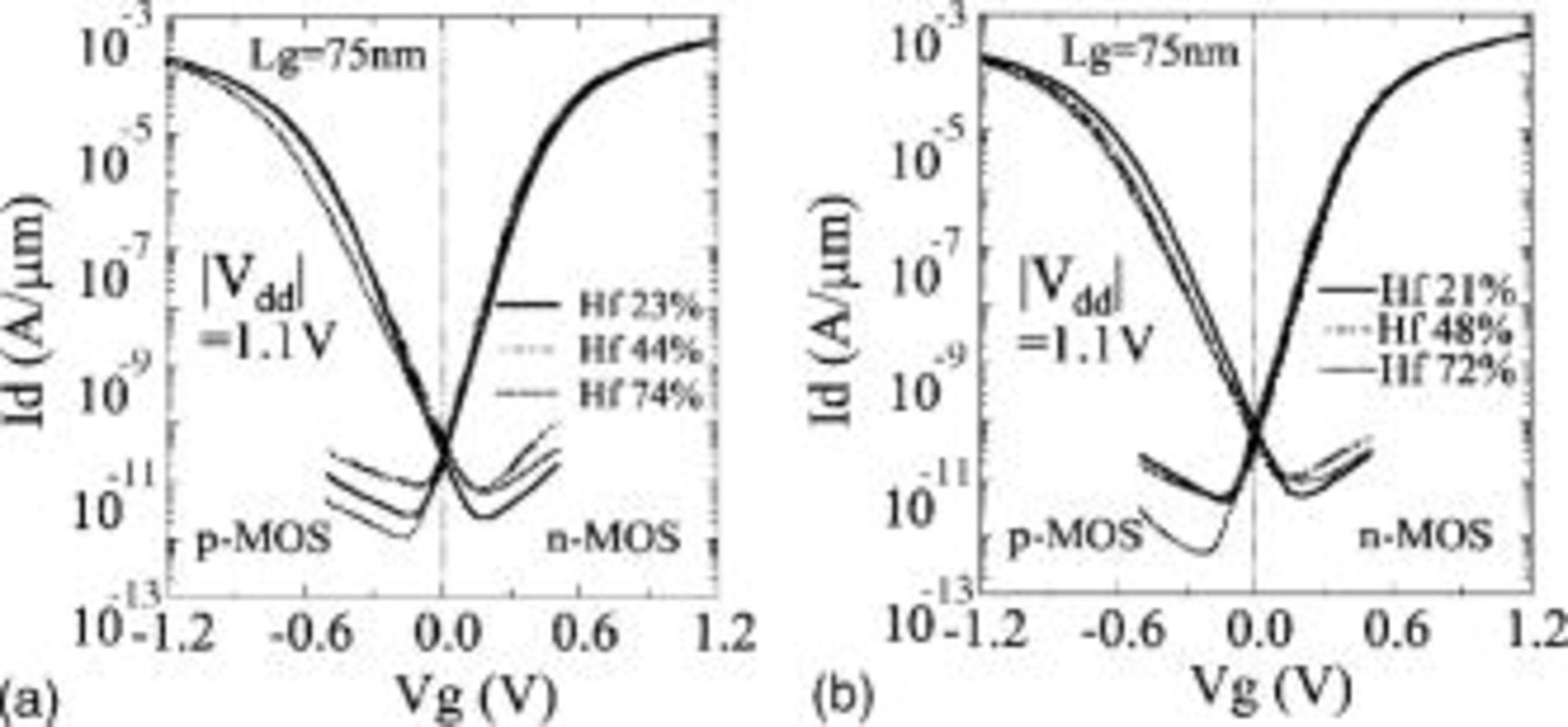
Figure 4. Subthreshold characteristics of ALD Hf-silicate gate stacks with different Hf contents, using (a) TDMAS and (b) BDMAS precursors. In this (Lg) and the gate width  of the transistors used were
  and
and  , and the applied voltages between the drain and the source were 1.1 and
  for the n- and p-MOSFETs, respectively. The value of the threshold voltage was defined as the gate voltage for
  for n- and p-MOSFETs.
Table I. Processing parameters and electrical properties of ALD Hf-silicate gate stacks using TDMAS and BDMAS precursors.
| Si Precorsors |
 ratio ratio |
 composition composition |
  at at 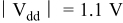
|
  at at 
| S (mV/dec.) | |||
|---|---|---|---|---|---|---|---|---|
| n-MOS | p-MOS | n-MOS | p-MOS | p-MOS | p-MOS | |||

| 23% | 320 | 152 | 20 | 30 | 74 | 92 | |
| TDMAS |

| 44% | 352 | 155 | 26 | 60 | 72 | 96 |

| 74% | 340 | 118 | 29 | 45 | 71 | 102 | |

| 21% | 379 | 159 | 52 | 62 | 75 | 94 | |
| BDMAS |

| 48% | 389 | 134 | 31 | 43 | 73 | 99 |

| 72% | 390 | 115 | 74 | 66 | 74 | 105 | |
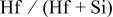
Figure 5 shows the effective mobility curves of ALD Hf-silicate gate stacks employing TDMAS for (a) n-MOSFETs and (b) p-MOSFETs. Universal curves are shown for reference. Hf-silicate films were evaluated with three different Hf contents (Hf 74% using  , Hf 44% using
  , and Hf 23% using
  ratio). The effective mobility was measured by applying a modified split C-V method. As shown in Fig. 5, the effective curves were good for both n-MOS and p-MOSFETs, being the same level as that of reference universal curves at
  . Furthermore, the effective mobility curves did not vary between the Hf contents [
 23–74%] for either n-MOS and p-MOSFETs.
Figure 5. Effective mobility curves of ALD Hf-silicate gate stacks employing TDMAS for (a) n-MOSFETs and (b) p-MOSFETs. Universal curves are shown for reference. Hf-silicate films were evaluated with three different Hf contents (Hf 74% using  , Hf 44% using
  , and Hf 23% using
  ratio). The effective mobility was measured by applying a modified split C-V method.
Figure 6 shows the effective mobility curves of ALD Hf-silicate gate stacks employing BDMAS for (a) n-MOSFETs and (b) p-MOSFETs. Hf-silicate films were evaluated with three different Hf contents (Hf 72% using  , Hf 48% using
  , and Hf 21% using
  ratio). The effective curves were good for both n-MOS and p-MOSFETs, and the effective mobility curves did not vary between the Hf contents (
 21–72%) for either n-MOS or p-MOSFETs. Also, the effective mobility curves of Hf-silicate gate stacks employing BDMAS were almost the same as those employing TDMAS (Fig. 5) for all of the n-MOS and p-MOSFETs.
Figure 6. Effective mobility curves of ALD Hf-silicate gate stacks employing BDMAS for (a) n-MOSFETs and (b) p-MOSFETs. Hf-silicate films were evaluated with three different Hf contents (Hf 72% using  , Hf 48% using
  , and Hf 21% using
  ratio).
Figure 7 shows the number of interface trap density (Nit) of ALD Hf-silicate gate stacks employing (a) TDMAS and (b) BDMAS for both n-MOS and p-MOSFETs. As shown in Fig. 7, the interface trap densities for all n-MOSFET devices were low, despite using high- gate stacks. Trap densities of about
  for all n-MOSFETs were almost the same level as those with the
  SiON reference film.14, 23 Therefore, the effective mobility curves did not vary between the Hf contents [
 21–74%] and using TDMAS and BDMAS precursors for n-MOSFETs. However, the interface trap densities for all p-MOSFET devices were higher than those with the
  SiON reference film. For p-MOSFETs, the effective mobility is not so sensitive to the interface trap density, so the effective mobility is not changed for all ALD Hf-silicate gate stacks employing TDMAS and BDMAS precursors (Fig. 5 and 6).
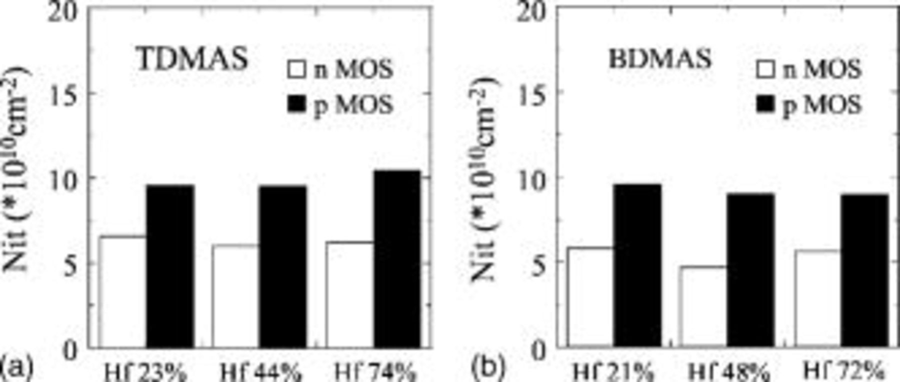
Figure 7. Interface trap density (Nit) of ALD Hf-silicate gate stacks employing (a) TDMAS and (b) BDMAS for both n-MOS and p-MOSFETs. Nit was evaluated from the charge-pumping current (Icp) at room temperature. In this measurement, the gate length (Lg) and the gate width  used were 0.5 and
  , respectively.
Figure 8 shows the leakage current density at  as a function of EOT for n-MOSFETs. Thermal oxide data is also given for reference. The I-V measurements were performed using capacitors with an area of
 . The leakage current density in Hf-silicate gate stacks with
  were reduced by about 3 orders of the magnitude with respect to a reference
  film. Furthermore, the leakage current densities were dependent on the Hf content of the Hf-silicate gate stacks: the leakage current densities were reduced as the Hf content increased because all of the devices were fabricated with same thickness, resulting in thinner EOTs. Furthermore, the leakage current densities were not dependent on the Si precursors.
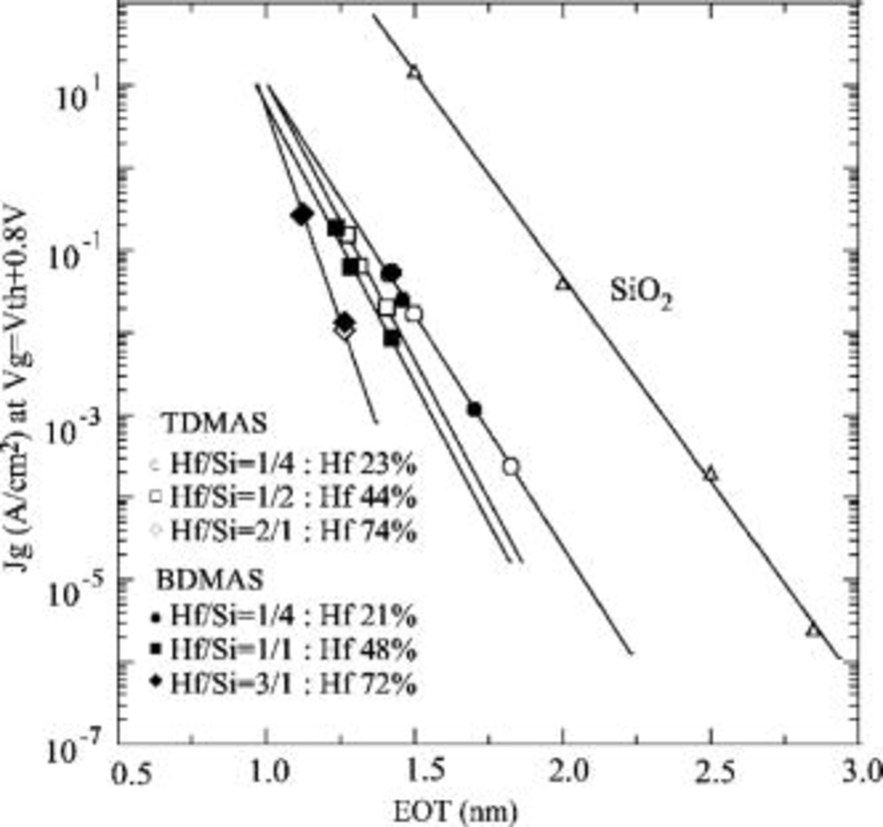
Figure 8. Leakage current density at  as a function of EOT for n-MOSFETs. I-V measurements were performed using capacitors with an area of
 .
.
Figure 9 shows SIMS depth profiles of ALD Hf-silicate films using (a) TDMAS and (b) BDMAS precursors. In these results, a  ratio of 1:1 was used in each ALD Hf-silicate film formation, and all the films were deposited at
  . The
. The  compositions of the Hf-silicate films were 56 and 48% using TDMAS and BDMAS, respectively. As can be seen in Fig. 9a-1, the average residual carbon impurity concentrations in the as-deposited layer using TDMAS were
  . For ALD Hf-silicate film formation using BDMAS (as shown in Fig. 9a-2), the carbon impurity concentrations were reduced by about an order of magnitude with respect to the process using TDMAS. As shown in Fig. 9b-1 and 9b-2, the average residual carbon impurity concentrations in the annealed layer, using both Si precursors, were reduced by about a half order of magnitude compared with the as-deposited layers. Furthermore, as the carbon impurity concentrations near the surface of the annealed layers were about
  for both Si precursors, it was considered that the electrical properties would be almost the same for the Hf-silicate gate stacks with the same Hf content.
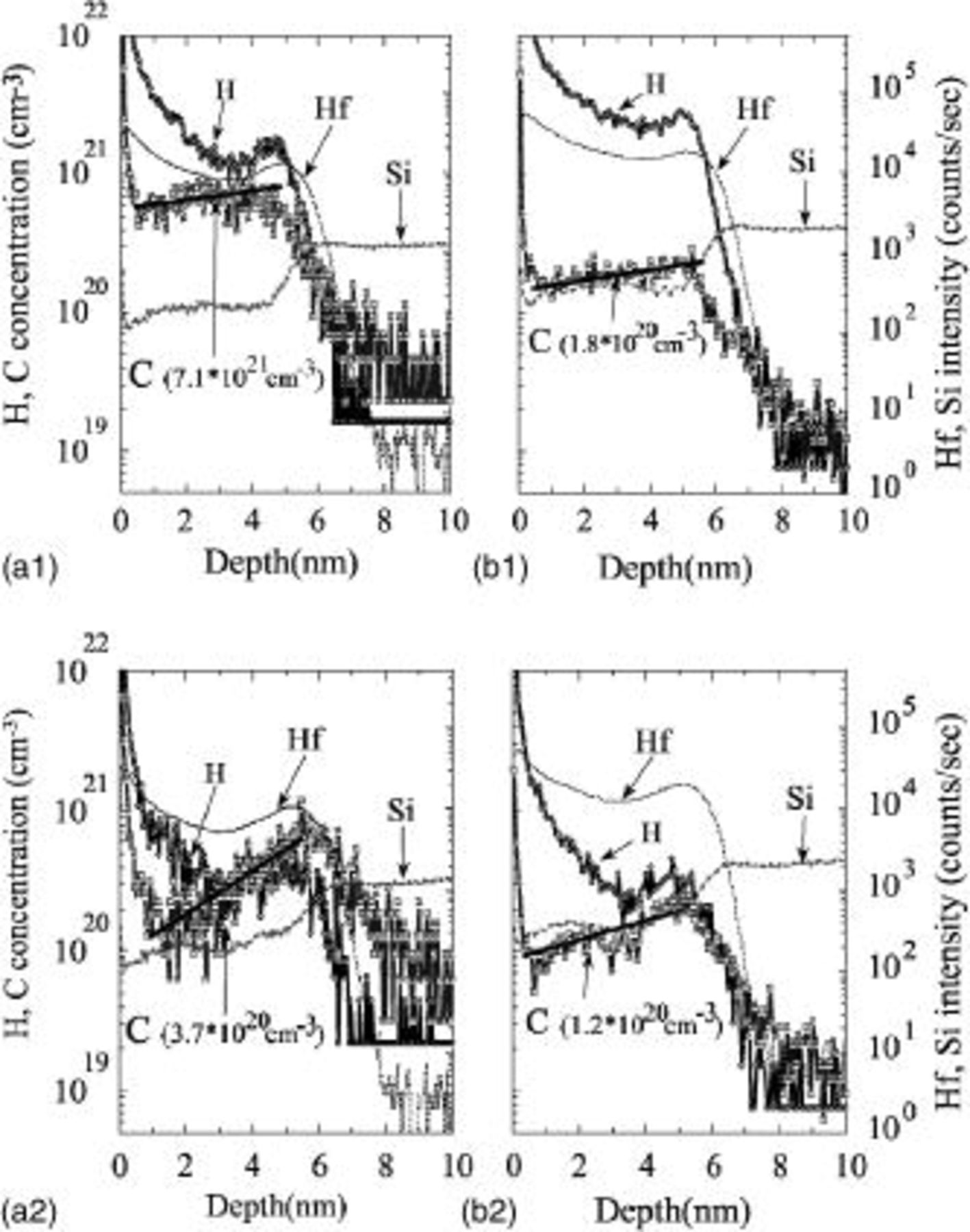
Figure 9. SIMS depth profiles of ALD Hf-silicate films using TDMAS (a) and BDMAS (b) precursors. (a-1) and (b-1) The as-deposited case, and (a-2) and (b-2) that treated by high-temperature annealing at  for
for  in
in  -diluted oxygen atmosphere (
 concentration of 0.1%), respectively.
  ratios of 1:1 were used in each ALD Hf-silicate film formation and all the films were deposited at
  . SIMS analyses were done with a
  cesium primary ion
  beam. The concentrations
  of carbon and hydrogen impurities are indicated by the left ordinate and the secondary ion intensities of Hf and Si (counts/s) are indicated by the right ordinate.
Conclusions
We investigated the electrical properties of poly-Si/ALD Hf-silicate gate stacks fabricated using BDMAS and TDMAS precursors. The high- films were fabricated using atomic layer deposition (ALD) employing
  and each of the Si precursors, in which the
  composition was controlled. The EOTs were reduced in line with increasing Hf contents: the very thin dielectric
  was fabricated with a
  composition of 74%. The
  shifts of p-MOSFETs were improved by reducing the
  composition: the value of the
  shifts was improved to about
  for Hf-silicate gate stacks in which
  composition was reduced from 72–74% to 21–23%. The subthreshold swings were dependent on the Hf content in the p-MOSFETs for both Si precursors.
  values were varied from
  /dec for
  compositions from 21 to 74%, respectively, due to the Fermi-level pinning problem
  . Inspecting the subthreshold characteristics of n-MOSFETs, the values of
  at
at  were greater than
  and
and  was lower than
  with both Si precursors
  . With p-MOSFETs, the values of
  at
at  for Hf-silicate gate stacks in which
  was about
  greater than those in which
  . The leakage current densities were dependent on the Hf content in the Hf-silicate gate stacks. However, those were independent of the Si precursors for the Hf-silicate gate stacks with the same Hf content, because the carbon impurity concentrations near the surface of the annealed layers at
  were about
  for both Si precursors.
Acknowledgment
The authors thank Dr. K. Nakamura for his encouragement and useful discussions.
Semiconductor Leading Edge Technologies (Selete), Incorporated, assisted in meeting the publication costs of this article.