
Abstract
The authors report the growth of TiO2 nanowires by heating the Ti/glass template and the fabrication of a TiO2 nanowire photodetector (PD) by depositing interdigitated contact electrodes. It was also found that the fabricated TiO2 nanowire PD was visible-blind with a cutoff wavelength around 390 nm. Compared with conventional film-type TiO2 PDs, it was found that we could achieve a 10 times larger photocurrent from the TiO2 nanowire PD. It was also found that dynamic response of the TiO2 nanowire PD was stable and reproducible with an on/off current contrast ratio of around 100. Furthermore, it was found that UV-to-visible rejection ratio observed from the TiO2 nanowire PD was also larger, as compared to conventional film-type TiO2 PDs.
Export citation and abstract BibTeX RIS
Ultraviolet (UV) photodetectors (PDs) are important devices that can be used in various applications such as space communication, ozone-layer monitoring, and flame detection. With improved growth and processing technologies, UV PDs using Si as the active layer have already been successfully commercialized. However, the responsivity of Si PDs in UV region is low due to its small bandgap energy.1 At the same time, Si-based PDs also detect visible light (i.e., 400–700 nm). In many applications, it is important to detect UV light without also detecting visible light. In order to achieve "visible-blind," one needs to push the cutoff wavelength to λ ≦ 400 nm. With bandgap energy of 3.0 eV (for rutile), the cutoff wavelength for TiO2 is around 390 nm.2,3 For the fabrication of visible-blind PDs, TiO2 is a good candidate material.
TiO2 is an interesting semiconductor material that has attracted much attention in recent years. It has been shown that thin-film TiO2 can be used for gas sensors,4,5 light emission diode,6,7 and solar cells.8–10 With a wide direct bandgap energy of 3.0 eV, planar-type TiO2-based PDs have also been demonstrated.2,3 Other than planar films, it is also possible to fabricate TiO2 nanowire-based PDs. One-dimensional (1-D) semiconductor nanowires have attracted great attention because of their potential applications in nanoscale devices. Compared with bulk or thin film-based devices, 1-D nanowire PDs should provide a high internal photoconductivity gain due to the surface-enhanced electron-hole separation efficiency.11,12
Recently, TiO2 nanowires have attracted a lot of attention for potential application in optoelectronic devices due to their large surface-area-to-volume ratio. Wu et al. reported the growth of TiO2 nanowires on glass substrates by thermal evaporation.13,14 They produced single-crystalline TiO2 NWs, whose size and density were controlled by adjusting the growth parameters. The electron field emitter also has been fabricated. However, no report on the fabrication of 1-D TiO2 nanowire PDs could be found in the literature, to our knowledge. In this study, we report the growth of TiO2 nanowires by the furnace oxidation of Ti/glass template. The visible-blind TiO2 nanowire PDs also were fabricated. Physical properties of the nanowires and electrooptical properties of the fabricated PDs will also be discussed.
Experimental
Before the growth of the TiO2 nanowires, a Corning 1737 glass substrate was wet-cleaned with acetone and de-ionized water. The glass substrate was subsequently baked at 100°C for 10 min to evacuate moisture. A 400-nm-thick titanium (Ti) film layer was then deposited onto the glass substrate by electron-beam evaporation. Finally, the samples were annealed in a furnace at 700°C for 3 hours to synthesize TiO2 nanowires in argon (Ar) ambiance. The crystal quality of the as-grown nanowires was then characterized by an X-ray diffractometer (XRD, MAC MXP18) and a high resolution transmission electron microscope (HRTEM, JEOL JEM-2100F). The surface morphology of the samples and the size distribution of the nanowires were characterized by a field-emission scanning electron microscope (FE-SEM, JEOL JSM-7000F).
To fabricate the TiO2 nanowire UV PD, we deposited a thick Pt (100 nm) film through an interdigitated shadow mask onto the TiO2 nanowires to serve as contact electrodes, as shown in Figure 1. We designed the size of interdigitated shadow mask as 2 mm wide and 2.2 mm long with a finger spacing of 0.2 mm. A conventional 2-D TiO2 PD prepared on glass substrate by sputtering was also fabricated for comparison. It should be noted that identical interdigitated shadow mask and exactly the same Pt (100 nm) contact electrodes were used for the 2-D TiO2 PD. Current-voltage (I-V) characteristics of the fabricated PDs were then measured by an HP 4156 semiconductor parameter analyzer at room temperature. Spectral-responsivity measurements of the PDs were also performed at room temperature by a JOBIN-YVON SPEX System with a 300-W xenon arc lamp light source (PERKINELMER PE300BUV) and a standard synchronous detection scheme.
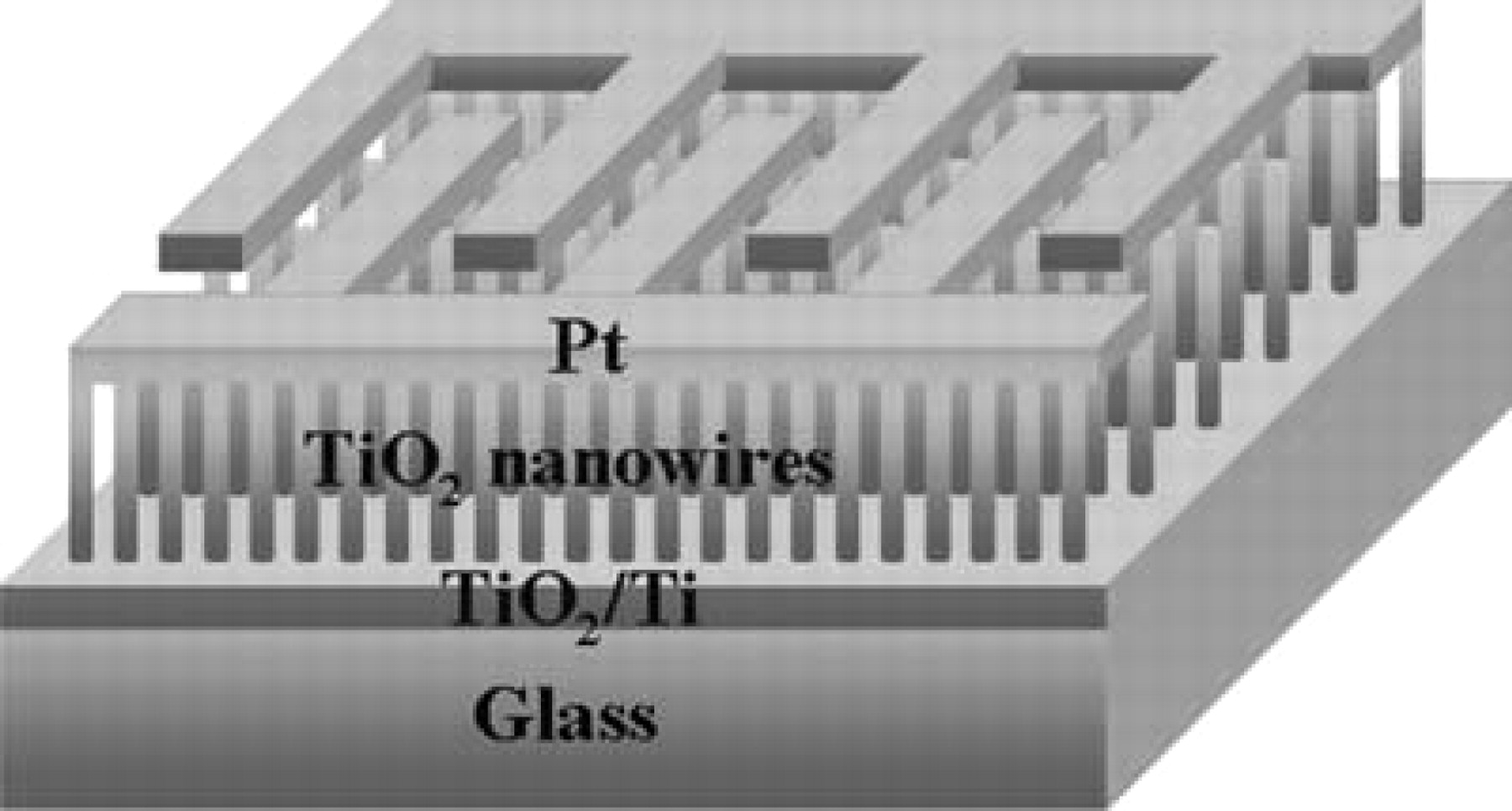
Figure 1. Schematic diagram of the fabricated TiO2 nanowire PD.
Results and Discussion
Figure 2a shows a cross-sectional FE-SEM image of the nanowires prepared on a Ti/glass template. It can be clearly seen that high-density nanowires were grown on the Ti/glass template. As shown in Fig. 2a, the average length and average diameter of these nanowires are 0.3 μm and 50 nm, respectively. Figure 2b shows the crystallographic characteristics obtained from XRD measurements. As shown in Figure 2b, it was found that the sharp XRD peak was observed from the nanowires could be indexed to (110) of rutile-TiO2 (JCPDS Card no. 88-1175). No Ti-related signal was found, indicating that the Ti film changed into TiO2 nanowires after the furnace oxide annealing process. It also was found that only one XRD peak was observed from the TiO2 nanowires. It was noticed that the TiO2 nanowires grown by the method of furnace oxidation were single crystalline. Figure 3a shows the bright-field TEM image of the as-grown TiO2 nanowires while Figure 3b shows the HRTEM image of the individual TiO2 nanowire. The images clearly show the single crystalline structure of the nanowire. The inter-planar spacing is 3.2 Å, which corresponds to the spacing of (110) for rutile-TiO2. The inset of Figure 3b shows the selected-area electron diffraction (SAED) pattern of the nanowire. The electron diffraction pattern also shows that the nanowire is uniformly crystalline.
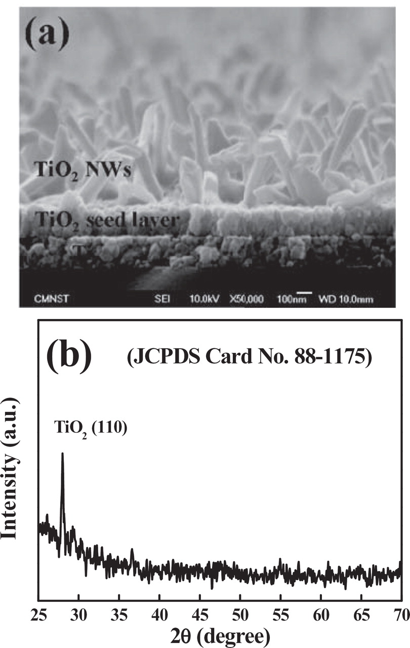
Figure 2. (a) Cross-sectional FE-SEM images of TiO2 nanowires and (b) XRD analysis of TiO2 nanowires.
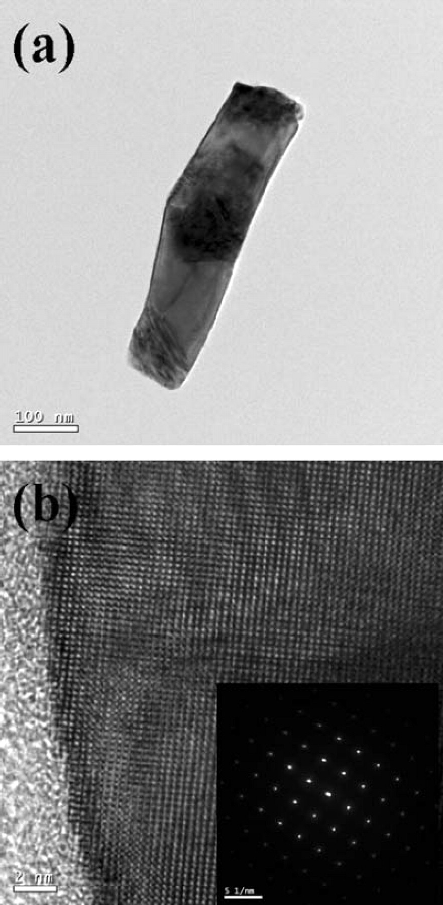
Figure 3. (a) Bright-field TEM image of the TiO2 nanowire. (b) A high-resolution TEM image of individual TiO2 nanowire in (a). The inset in (b) shows the SAED patterns.
Figure 4 shows I-V characteristics of the fabricated TiO2 nanowire PD measured in dark and under UV illumination. During photocurrent measurement, we illuminated the sample with 390-nm UV light (0.54 mW/cm2) by dispersing a 300-W xenon arc lamp with a monochromator. For comparison, I-V characteristics of the conventional 2-D TiO2 PD were also plotted. With 5 V applied bias, it was found that dark currents measured from conventional 2-D TiO2 PD and TiO2 nanowire PD were 1.24 × 10⁻¹⁰ and 2.97 × 10⁻¹¹ A, respectively. The low dark currents observed from both PDs could be attributed to the barrier height of the Pt/TiO2 contact. It was also found that the dark current of TiO2 nanowire PD was lower than 2-D TiO2 PD. The small dark current should be attributed to the high resistance and good crystal quality of the single crystalline TiO2 nanowires. Under the same applied bias, it was found that the measured photocurrents increased to 3.03 × 10⁻¹⁰ and 1.62 × 10⁻⁹ A for the conventional 2-D TiO2 PD and TiO2 nanowire PD, respectively. In other words, we achieved an almost 10 times larger photocurrent from the TiO2 nanowire PD, as compared to that observed from the conventional 2-D TiO2 PD. The significantly larger photocurrent also provides us a much larger photocurrent to dark current contrast ratio for TiO2 nanowire PD.
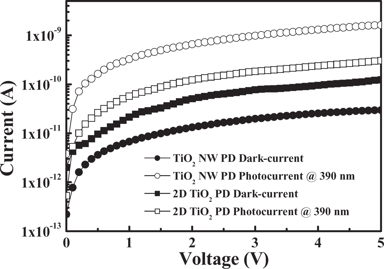
Figure 4. Room-temperature I-V characteristics of the TiO2 PDs measured in dark and under 390 nm UV illumination.
Figure 5 shows measured transient response of the fabricated TiO2 nanowire PD, as we switched the UV excitation on and off. The on and off times of the light source was both controlled at 120 seconds. As shown in Figure 5, it was found that dynamic response of the TiO2 nanowire PD was stable and reproducible with an on/off current contrast ratio of around 100. It was also found that photocurrent increased rapidly initially and then increased much slower as we turned on the UV excitation. Similar slow response was also observed as we turned off the UV light. With a rough nanowire surface, the surface defect related trapping center could retard the speeds of charge-carrier collection upon UV illumination and charge-carrier recombination as the UV light was turned off.15
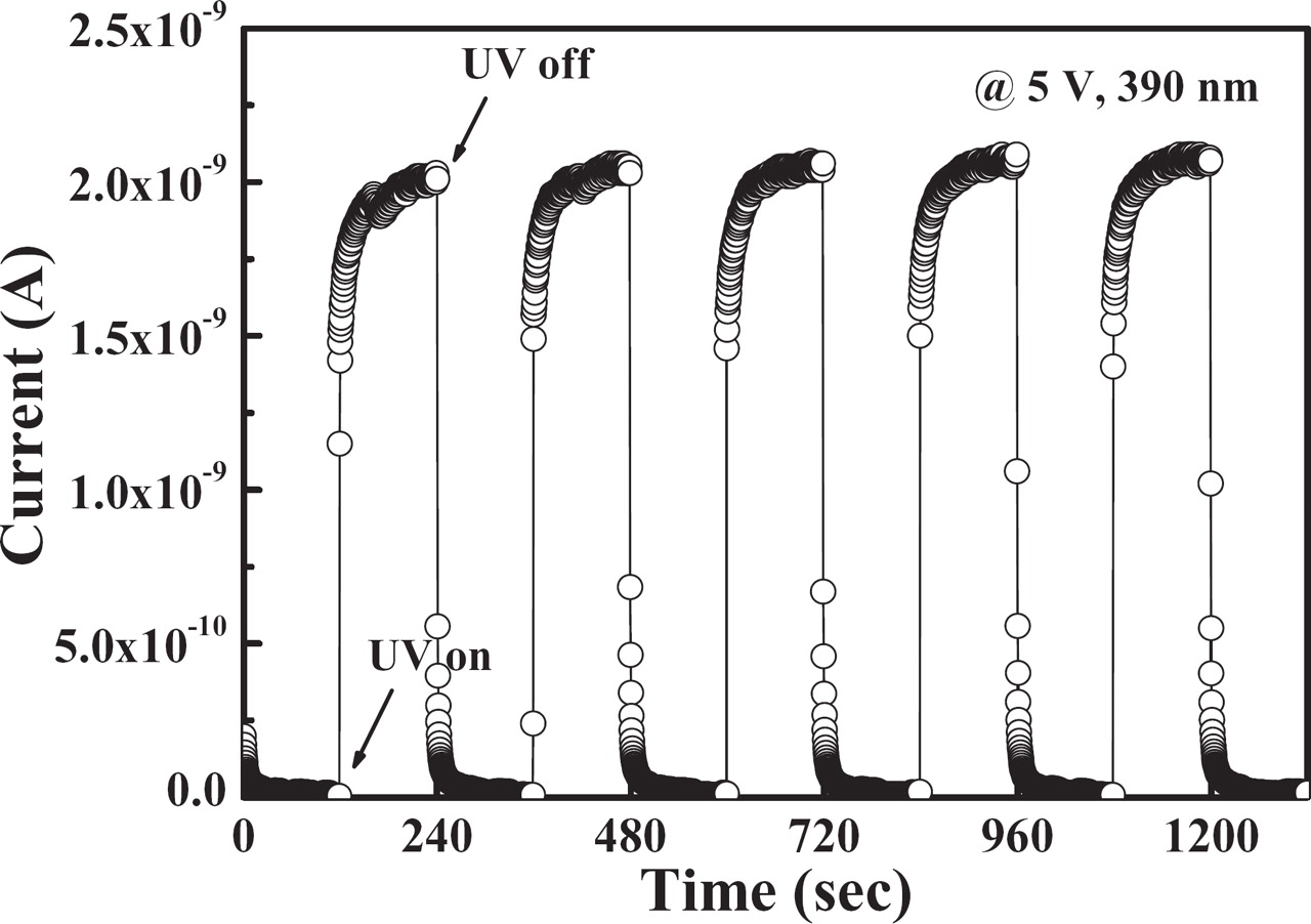
Figure 5. Transient response of the fabricated TiO2 nanowire PD, as we switched the UV excitation on and off.
Figure 6 shows room-temperature spectral responses of the fabricated TiO2 nanowire PD using a 300-W Xe lamp dispersed by a monochromator as the excitation source. During these measurements, the monochromatic light calibrated with a UV-enhanced Si diode and an optical power meter was modulated by a mechanical chopper and collimated onto the front-side (i.e., metal-side) of the fabricated devices using an optical fiber. The photocurrent was then recorded by a lock-in amplifier. It should be noted that photoresponses of the fabricated PD were flat in the short-wavelength region while a cutoff wavelength occurred at around 390 nm. This indicates that the fabricated TiO2 nanowire PD was indeed visible-blind. With an incident light wavelength of 390 nm and a 5 V applied bias, it was found that the measured responsivities were 6.85 × 10⁻² and 7.65 × 10⁻³ mA/W for the TiO2 nanowire PD and the conventional 2-D TiO2 PD, respectively. In other words, we achieved a around 10 times larger responsivity from the TiO2 NW PD, as compared to that observed from conventional 2-D TiO2 PD. It is possible that the extra absorption is partially attributed to the additional TiO2 NW layer and/or to the surface roughness. As shown in Figure 6, it can also be observed clearly that measured responsivity increased as applied bias increased on the TiO2 nanowire PD. This suggests that photoconductive gain exists in the TiO2 nanowire PD.16 Recently, high photoconductive gain has also been observed from ZnO17 and SnO218 nanowire PDs. It has been shown that the photoconductive gain in these oxide semiconductor nanowires was related to the molecular sensitization mechanism and/or hole-trapping effect.17,18 Similar phenomena should also occur in our TiO2 nanowire PD. In the dark, oxygen molecules absorb on the nanowire surface and capture free electrons from the n-type TiO2. Therefore, it creates a depletion layer with low conductivity near the surface. Under 390-nm UV irradiation, electron-hole pairs will be generated in the depletion region. The photogenerated holes oxidize the adsorbed negatively charged oxygen ions on the surface while the remaining electrons in the conduction band increase the conductivity. These oxygen-related hole-trap states at the nanowire surface prevent charge-carrier recombination and prolong the photocarrier lifetime. Recently, Ji et al. report the fabrication of ZnO nanorod UV PDs.19 It was found that ZnO nanorod PDs can provide a higher responsivity and a larger UV-to-visible rejection ratio than the conventional 2D ZnO PDs. Compared to their results, it should be noted that the performances of this TiO2 nanowire PD were not optimized. We believe the low responsivity was related to the poor carrier collection efficiency from the electrodes since the 0.2 mm finger spacing was too long. We should be able to achieve a much larger responsivity by optimizing the fabricated parameters of the TiO2 nanowire PD. Here, we define UV-to-visible rejection ratio as the responsivity measured at 350 nm divided by the responsivity measured at 450 nm. With such a definition, it was found that the UV-to-visible rejection ratios were 15 and 3 for the TiO2 nanowire PD and conventional 2-D TiO2 PD, respectively, when biased at 5 V.
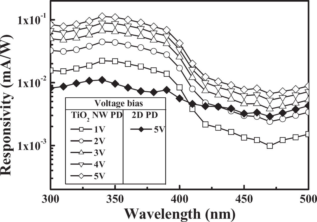
Figure 6. Room-temperature spectral responses of the TiO2 PDs measured with different applied biases.
Conclusions
In summary, we report the growth of TiO2 nanowires by heating the Ti/glass template and the fabrication of a TiO2 nanowire PD by depositing interdigitated contact electrodes. It was found that the average length and diameter of the TiO2 nanowires were around 0.3 um and 50 nm, respectively. It was also found that the fabricated TiO2 nanowire PD was visible-blind with a cutoff wavelength around 390 nm. Compared with conventional film-type TiO2 PDs, it was found that we could achieve a 10 times larger photocurrent from the TiO2 nanowire PD. It was also found that dynamic response of the TiO2 nanowire PD was stable and reproducible with an on/off current contrast ratio of around 100. Furthermore, it was found that UV-to-visible rejection ratio observed from the TiO2 nanowire PD was also larger, as compared to conventional 2-D TiO2 PDs.