
Abstract
We report an investigation of the leakage current in Pt/β-Ga2O3 Schottky contacts on an ( ) substrate using a temperature-dependent current–voltage (I-V-T) measurement in a temperature range of 300 K to 425 K. It was revealed that the main process of the reverse leakage current flow is the emission of electrons through trap states located near the metal-semiconductor interface, governed by the Poole-Frenkel emission (PFE). Based on an etch pits analysis, the density of the defects at the surface of the (
 ) β-Ga2O3 substrates was estimated to be ∼2 × 105 cm−2. The trap states associated with these high-density defects, which could be the main culprit for the reverse leakage current in the Pt/β-Ga2O3 Schottky contacts, were identified at ∼ 0.7 eV below the conduction band.
Export citation and abstract BibTeX RIS

This is an open access article distributed under the terms of the Creative Commons Attribution Non-Commercial No Derivatives 4.0 License (CC BY-NC-ND, http://creativecommons.org/licenses/by-nc-nd/4.0/), which permits non-commercial reuse, distribution, and reproduction in any medium, provided the original work is not changed in any way and is properly cited. For permission for commercial reuse, please email: oa@electrochem.org.
Gallium oxide (Ga2O3) has attracted great attention as a promising material platform for power devices and optoelectronics due to its superior material properties, such as an ultra-wide bandgap of approximately 4.9 eV and a high breakdown electric field of up to 8 MV/cm.1–4 In addition, the availability of large-size single-crystal β-Ga2O3 wafers fabricated by a low-cost edge-defined film-fed growth (EFG) method will enable the future mass production of β-Ga2O3-based devices including Schottky barrier diodes (SBDs) and field-effect transistors (FETs).5,6 The β-Ga2O3 SBDs have showed great potential for high power applications.7 However, crystal defects such as oxygen vacancies, dislocations and point defects8–11 are generally present at high densities in the β-Ga2O3 wafers since the EFG technique is less mature so far. The defects in material have widely been known to cause a serious leakage current issue in a device, degrading its performance and reliability. Therefore, to understand the fundamentals of current transport in the metal/semiconductor junction is of great importance for the development of high performance devices based on β-Ga2O3.12 Recently, Masataka Higashiwaki et al. demonstrated high-voltage vertical SBDs by epitaxy of an n−-β-Ga2O3 drift layer on (001) substrates and revealed that the reverse leakage current is associated with crystal defects by a thermionic field emission (TEF) model.13,14 Kasu et al. also reported their study on the correlation between crystal defects and leakage current in the Schottky contacts to (010), (001) and ( )-oriented β-Ga2O3 substrates,9–11 but without explaining the underlying leakage mechanisms. The leakage analysis for Schottky contacts to β-Ga2O3 is still quit limited in the literature.
In this letter, we report on a study of leakage current in Pt Schottky contacts to an EFG-grown  β-Ga2O3 substrate by a temperature-dependent current–voltage (I-V-T) measurement. The reverse leakage current in a temperature range of 300 K to 425 K was found to be in agreement with the Pool-Frenkel emission (PFE) theory.
Experimental
Two pieces of ( ) β-Ga2O3 substrates were prepared from a bulk crystal grown by the EFG method in this study. The Ga2O3 powder 99.995% in purity was used as the source material. The crystal was grown in the <010> direction, with a growth rate adjusted to 6–10 mm/h, in the atmosphere mixture of argon and carbon dioxide. After cutting the substrates about 1 mm in thickness and 10 × 10 mm2 in size, a high temperature annealing at 1500 °C was performed in air for 48 hours to reduce residual stress in the crystal and improve their crystalline quality. And the surfaces of the substrates were treated by a double-side chemical mechanical polishing (CMP) process. Vertical SBDs were fabricated using one piece of the substrates. First, the substrate was cleaned with acetone and isopropanol, followed by a 4-cycle deionized (DI) water rinse and N2 blow drying. After that, ohmic metal was deposited on back side of the sample by blanket evaporation of Ti/Au (50 nm/250 nm). To facilitate the formation of a good ohmic contact between Ti and β-Ga2O3, a rapid thermal annealing at 850°C for 30 seconds in a N2 ambient was performed. Then, a Pt/Ti/Au (50 nm/50 nm/150 nm) metal stack was evaporated on the front side of the sample and patterned using a liftoff process, serving as the Schottky electrodes. Fig. 1 schematically illustrates the device structure of the fabricated SBDs. The diameter of the circular Schottky contacts was 200 μm. The sample was attached onto a copper plate by using conductive silver paste and a Keithley 4200 parameter analyzer was employed for the current–voltage (I-V) and capacitance-voltage (C-V) characterization. The I-V-T measurements were performed under a vacuum of ∼ 10−4 Pa.
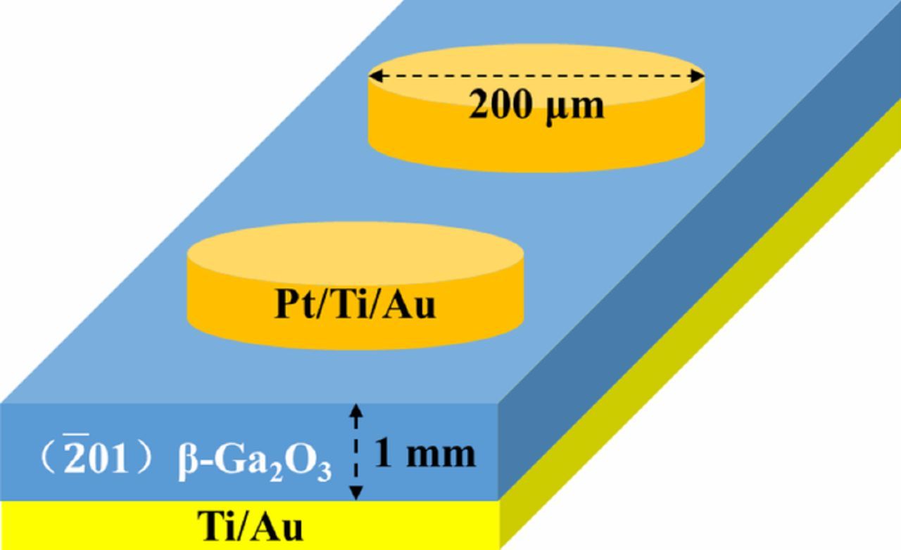
Figure 1. Schematic device structure of the vertical Pt/β-Ga2O3 SBDs.
Results and Discussion
Fig. 2 shows the typical I-V characterization of a fabricated Pt/β-Ga2O3 SBD at 300 K. The device exhibited a good rectification characteristic with a reverse leakage current density of ∼10−3 A/cm2 at a reverse bias of −20 V and a forward current density reaching 320 A/cm2 at a forward bias of 3.7 V. The ideality factor ns, the Schottky barrier height ϕB, and the series resistance RS were extracted from the forward I-V curve by using the following thermal emission (TE) model.
![Equation ([1])](https://content.cld.iop.org/journals/2162-8777/8/7/Q3054/revision1/d0001.gif)
where S is the area of the Schottky barrier contact, A* is effective Richardson's constant (33.7 A cm−2 K−2),15 q is the electron charge. The ns, ϕB, and RS were estimated to be 1.81, 1.27 eV, and 5.56 mΩ·cm2, respectively. The observed Schottky barrier height was lower than the theoretical value based on the electron affinity of Ga2O3 ∼ 4.00 eV15 and the work functions of Pt ∼ 5.93 eV.16 Besides, the ideality factor was much larger than unity. These could be due to the interface traps within the Schottky contacts and the barrier inhomogeneities.15,17 Fig. 3 shows the C-V characteristics for the fabricated devices measured at 100 kHz under 300 K. The effective donor concentration (Nd – Na) in the sample was extracted to be ∼ 4.03 × 1017 cm−3 from the linear fitting curve in the inset of Fig. 3. Apart from the shallow donor impurities like Si and Sn, it has been reported that plenty of oxygen vacancies usually exist within the β-Ga2O3 crystals and contribute to their n-type conductivity.8,18 The built-in voltage was extracted to be 2.42 V, which was much higher than the I-V determined schottky barrier height. This behavior was resulted from the existence of the defects in Ga2O3 and the barrier inhomogeneities in a noideal diode. Similar phenomenon was also observed by Yao et al.,19 which was associated with the observed large ideality factor in previous I-V results.
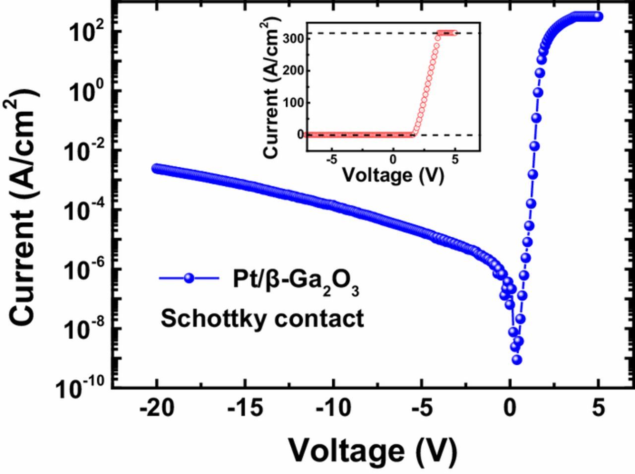
Figure 2. The typical I-V characterization of a fabricated Pt/β-Ga2O3 SBD at 300 K.
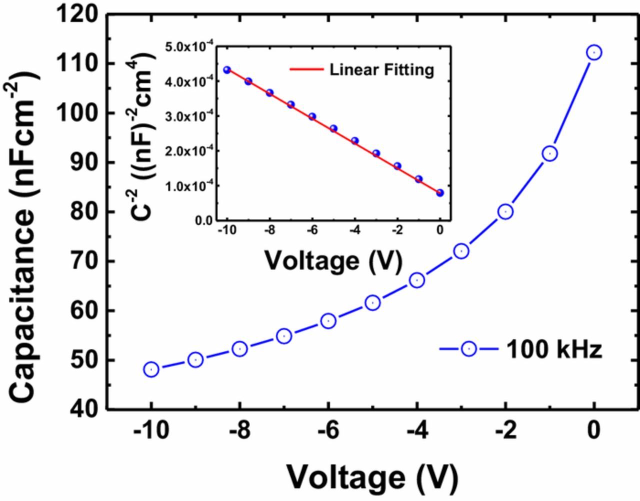
Figure 3. The typical C-V characterization of a fabricated Pt/β-Ga2O3 SBD at 300 K.
In order to reveal the crystal defects near the surface of ( ) β-Ga2O3 substrates, we carried out a wet etching process using the other piece of sample and observed its etch pits. The sample was first immersed in a 30% KOH solution at 90°C for 1 h. Then the etched surface was characterized by scanning electron microscopy (SEM). As shown in Fig. 4, etch pits with a distinctive shape can be clearly observed. The defects density of the (
 ) β-Ga2O3 substrates used in this study was estimated to be ∼ 2 × 105 cm−2. The KOH etched pits in our study were slightly different from those etched by H3PO4.9–11 We considered that these high-density defects must give rise to the reverse leakage current and the inhomogeneous barrier heights in the fabricated SBDs.
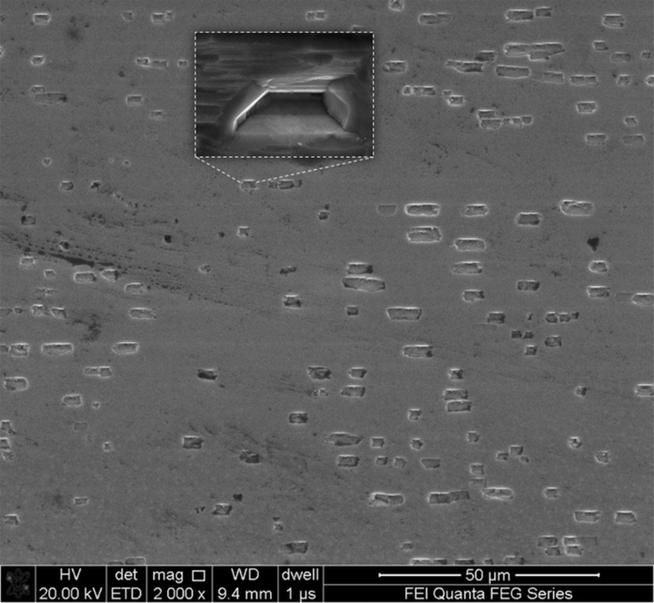
Figure 4. SEM image of the etched surface on the ( ) β-Ga2O3 substrate by hot KOH solution. The inset shows the enlarged image of an etched pit on the sample.
Fig. 5a shows the reverse I-V-T characteristics of the Pt/β-Ga2O3 SBD measured in a temperature range of 300 K to 425 K. The leakage current was observed to increase rapidly with the increase of both bias voltage and temperature, indicating an electric-field-enhanced thermal emission of the electrons within the reverse-biased Pt/β-Ga2O3 SBDs. We employed a PFE model to analyze the leakage mechanisms in the device. The PFE refers to the emission of electrons via a trap state into a continuum of electron states, which could be associated with the presence of defects.20–23 The PFE-governed leakage current density is given by
![Equation ([2])](https://content.cld.iop.org/journals/2162-8777/8/7/Q3054/revision1/d0002.gif)
where Eb is the electric field in the semiconductor barrier at the metal-semiconductor interface, ϕt is the barrier height of electron emission from the trap states, εr is the high-frequency relative dielectric constant, and C is a constant. As discussed in Ref. 22, r is the degree of compensation ranging from 1 to 2 depending on the position of Fermi level. Fig. 5b plots the log(J/Eb) versus  for the Pt/β-Ga2O3 SBD measured at various temperatures. The linear dependence of log(J/Eb) on
  is a proof for the PFE mechanism of the leakage current in the devices, as expressed by
![Equation ([3a])](https://content.cld.iop.org/journals/2162-8777/8/7/Q3054/revision1/d0003.gif)
![Equation ([3b])](https://content.cld.iop.org/journals/2162-8777/8/7/Q3054/revision1/d0004.gif)
![Equation ([3c])](https://content.cld.iop.org/journals/2162-8777/8/7/Q3054/revision1/d0005.gif)
![Equation ([3d])](https://content.cld.iop.org/journals/2162-8777/8/7/Q3054/revision1/d0006.gif)
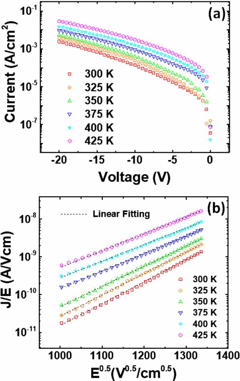
Figure 5. (a). The reverse I-V-T characteristics of the Pt/β-Ga2O3 SBD measured in a temperature range of 300 K to 425 K, (b). Poole-Frenkel plots of the reverse leakage current for the Pt/β-Ga2O3 SBD.
The m(T) and b(T) are plotted as functions of q/kT in Fig. 6. As defined in Eqs. (3c) and (3d), εr and ϕt can be calculated from the slop of m(T) and b(T) versus q/kT, respectively. Considering the β-Ga2O3 substrates in the experiment are relatively defective, it is fairly safe to choose r = 1 in the calculation.23 The obtained εr is 4.42, in good agreement with the reported value 3.91 for β-Ga2O3.24 From Fig. 6b, ϕt is calculated to be 0.7 V, suggesting that the trap states are probably located at ∼0.7 eV below the conduction band in the ( ) β-Ga2O3 substrates. Quite similarly, deep-level defects located at ∼ 0.8 eV below the conduction band have been recently revealed in the EFG-grown unintentionally-doped β-Ga2O3 by a steady-state photo-capacitance spectroscopy.25,26 These results further evidence the validity of using PFE model to describe the leakage current in our study. Therefore, it can be concluded that emission of electrons from metal into the defects-related trap states should be the dominant leakage mechanism in the Pt/β-Ga2O3 SBDs in the temperature range of 300 K to 425 K.
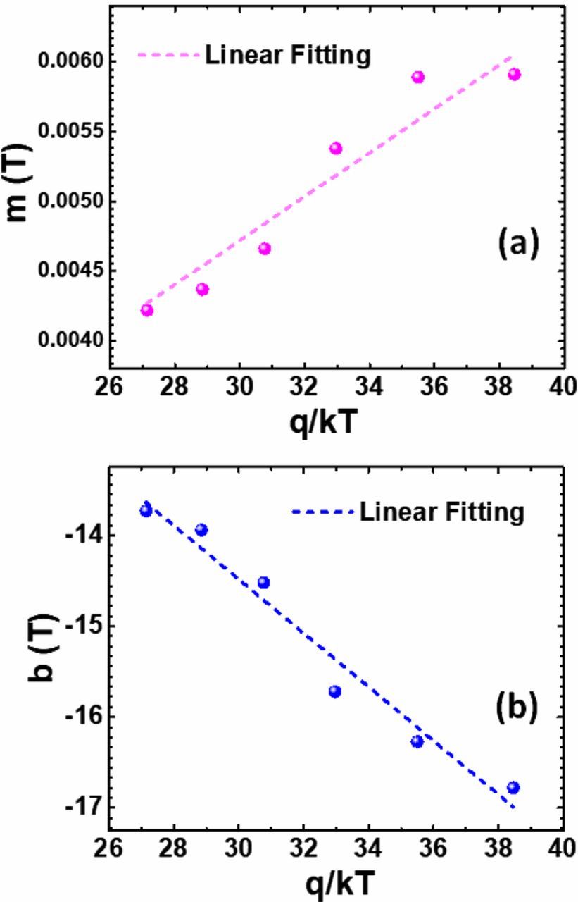
Figure 6. The m(T) and b(T) curves as functions of q/kT for the measured Pt/β-Ga2O3 SBD.
Conclusions
In summary, we fabricated Pt/β-Ga2O3 SBDs on an EFG-grown ( ) substrate and investigated the leakage current transport mechanism across the Schottky contacts through an I-V-T measurement. The fabricated SBDs showed a higher Schottky barrier height extracted by C-V measurement than that by I-V measurement, and a much larger ideality factor than one, indicating the existence of interface traps and the distribution of defect-induced barrier inhomogeneities of the devices. In the temperature range of 300 K to 425 K, the reverse leakage current could be well described by the PFE model, indicating a dominant leakage mechanism of the Pt/β-Ga2O3 SBDs by the emission of electrons via the detect-related trap states that located near the metal-semiconductor interface. The energy level of the defect-related trap states was deduced to be ∼0.7 eV below the conduction band for the EFG-grown (
 ) β-Ga2O3 substrates.
Acknowledgment
This work was supported in part by the Frontier and Key Technological Innovation Foundation of Guangdong Province under grant No. 2017A050506039, the International Science and Technology Cooperation Program of Guangzhou under grant No. 201807010093 and the National Natural Science Foundation of China under grant 11505140, 11375144 and 61621001.
ORCID
Leidang Zhou 0000-0003-3052-5556
Xing Lu 0000-0001-5808-9552