
Abstract
The shape of a silicon wafer is one of the key wafer characteristics. It is not only impacted by wafering and epitaxial processes but also highly modulated by device manufacturing processes, such as film deposition, CMP, lithography, and thermal process. Wafer shape can be best described and visualized by a complex 3D contour map, which contains both global (low spatial frequency) and local (high spatial frequency) wafer shape components. Unfortunately, the 3D contour map is not practical to guide wafer shape control in high volume production. To quantify and control the wafer shape, two global shape metrics, bow and warp, have been used for a few decades. These two metrics, however, are too simplified to capture local wafer shape. In this study, the limitations of traditional global shape metrics, bow and warp, are addressed, and different global and local shape metrics are explored. A novel shape metric of Site Slope-Radial Range (SSRR) reveals unique local wafer shape characteristics in the slope domain and may help us to better understand the impact of local wafer shape to device manufacturing processes, particularly lithography and CMP.
Export citation and abstract BibTeX RIS
The geometry of a bare silicon wafer as a starting substrate is critical to device manufacturing processes and final yield. Historically, wafer geometry has been characterized by various shape and flatness metrics defined by SEMI Shape Decision Tree and SEMI Flatness Decision Tree, respectively.1 Based on SEMI Standard M59, the shape for wafer surfaces is defined as the deviation of a specified wafer surface relative to a specified reference plane when the wafer is in an unclamped condition. Typically wafer shape captures the global component of wafer geometry with a spatial wavelength ranging from a few to hundreds of millimeters (Fig. 1). Directly derived from the device lithography application, wafer flatness is described by both global and local flatness metrics. Similar to global shape metrics, global flatness metrics, such as Global Backside Ideal Focal Plane Range (GBIR) measure the wafer thickness variation across the entire wafer. On the other hand, site flatness metrics, such as Site Frontside Least Squares Focal Plane Range (SFQR), capture local flatness variation within a site, which is usually governed by the device die size or scanner exposure slit size. The impact of site flatness of a bare wafer on lithography defocus and critical dimension (CD) uniformity is well understood.3,4 Over the years, the site flatness metric SFQR has become the most important parameter for incoming silicon wafer quality control, as reflected in both SEMI Standards M49 and ITRS1,5 in which the site flatness requirement is directly driven by the device CD scaling.
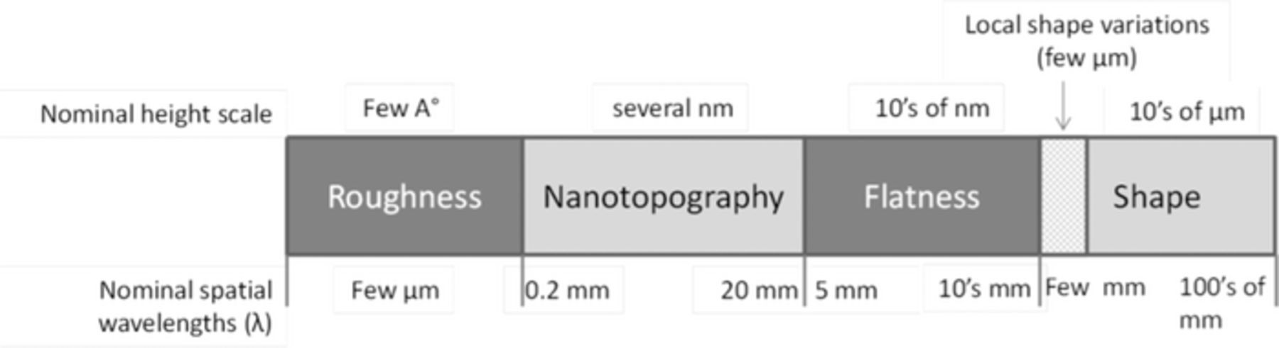
Figure 1. Nominal height scale vs. nominal spatial wavelength for different wafer geometry parameters.
With increasing device complexity and continuous shrinking of CD, the traditional wafer geometry metrics alone, defined in the thickness domain within FQA (flatness quality area), become insufficient. Since 1999, Intel-led metrology users' groups, with the participation of major silicon suppliers and key metrology suppliers, have been devoting significant effort to the development of wafer geometry metrologies and characterization metrics to meet the advanced technology needs.6 The extensive studies conducted by these users groups through close collaboration have enabled several critical, novel wafer geometry concepts for future silicon wafer development and high volume manufacturing (HVM) wafer quality control, including Nanotopography, Edge Roll-Off, Edge Dimension, and Localized Feature Metrics.7–8
Nanotopography is defined as the wafer surface topography in the spatial wavelength range of 0.2 millimeter to 20 millimeters (Figure 1).9 It is traditionally quantified by threshold height analysis (THA) curves at different analysis window areas (either 2 mm or 10 mm circular/square). THA values of 2 mm × 2 mm and 10 mm × 10 mm windows at the 0.05% threshold are most commonly used to monitor the surface nanotopography of incoming wafers. Since the introduction of nanotopography metrics, the surface topography of incoming wafers has improved tremendously, which has driven a significant enhancement of CMP and lithography performance.10–16
Historically, the edge dies on a wafer always yield lower compared to the center dies. To maximize the edge die yield, the wafer edge geometry characteristics need to be well understood. Edge Roll-Off metrics were developed to go beyond the conventional height domain, extending into the slope and curvature domains.8
In addition to near-edge geometry characterization, the optimization and standardization of wafer edge profile is important and has a direct impact to several device manufacturing processes. The edge profile metrics are defined to capture the key characteristics of an entire wafer edge profile, covering the front surface/bevel transition, bevel, and apex regions.
In the past decade, the continuous improvement of incoming wafer quality has shifted the focus to quantify process-induced local geometry features/defects, which could cause some issues in device manufacturing processes downstream. This has led to the development of a series of Localized Feature Metrics targeting known wafering or epitaxial growth induced localized geometry features in the areas of laser marks, wafer notch, and epitaxial susceptor pins.7
With the addition of Nanotopography, Edge-Roll-Off, Edge Dimension, and Localized Feature Metrics, the wafer geometry characterization becomes more comprehensive and moves to a new stage. However, our understanding of wafer shape, particularly local wafer shape, is still very limited. Insufficiency of the traditional wafer shape metrics was realized many years ago but no progress has been made over the past several decades. This study attempted to explore new approaches to characterize global and local wafer shape, particularly local shape in the slope domain.
Limitations of Traditional Wafer Shape Metrics
In bare silicon manufacturing, a wafer shape is dominated by wafering and epitaxial growth processes. When the wafer as a substrate goes through the device manufacturing processes, the wafer shape will continue changing in response to the device process-induced elastic and plastic deformation, such as film deposition, CMP, lithography, and thermal treatment.17,18 Some process steps, such as a uniform film deposition, could introduce a simple bowl shape containing mainly the low spatial frequency components; while the other process steps could lead to local shape variations such as a sharp slope change near the wafer edge. As a result of accumulative multiple process steps that a wafer has experienced, the wafer shape could end up with a complex contour which overlaps each individual process-induced shape component. Figure 2 demonstrates the shape contour maps of four bare silicon wafers. Due to different wafering and epitaxial growth processes, these four wafers have their own unique wafer shape characteristics.
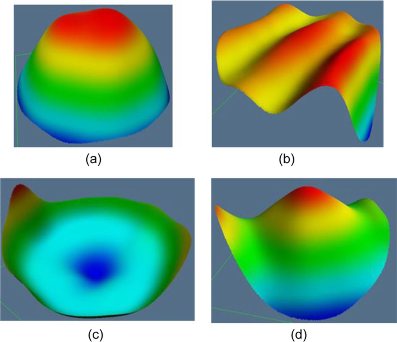
Figure 2. Wafer shape contour maps: (a) Wafer 1 with global inverted bowl shape, (b) Wafer 2 with a complex local variations in shape, (c) Wafer 3 with a lip near the edge, and (d) Wafer 4 with a saddle shape.
Traditionally, wafer shape is described by two global metrics, Bow and Warp. Of the wafer shape metrics, Bow-bf and Warp-bf have been used the most in the industry. Bow-bf is defined as the deviation of the center point of the wafer median surface with respect to a best-fit reference plane (see Figure 3). In SEMI M1, Warp-bf (GMLYMER) is defined as the global range metric of the median surface corrected for gravitational sag with respect to least squares reference plane1 as shown in Figure 3.
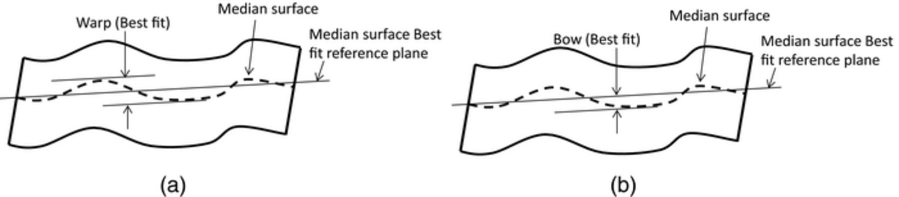
Figure 3. SEMI definitions of wafer shape parameters (a) Warp-bf, and (b) Bow-bf.
These two traditional shape metrics obviously are not sufficient to capture a complex wafer shape. There are three fundamental limitations of existing wafer shape metrics:19
First, these two traditional shape metrics are oversimplified. Since only one or two data points on a median surface plane are used to describe a wafer shape, they do not reflect the real complex wafer shape. Each of the four wafers shown in Figure 2 obviously has its own unique shape. However, all four wafers have similar Warp-bf values, and two of them even show similar Bow-bf values (Table I).
Table I. Bow and Warp values of the wafers used for the study.
| Wafer Number | Characteristics | Bow (μm) | Warp (μm) |
|---|---|---|---|
| 1 | Dome shape | 7 | 15 |
| 2 | Wafer with edge lip (down) | 1.5 | 14 |
| 3 | Wafer with edge lip (up) | −5 | 14 |
| 4 | Saddle shape | 6 | 15 |
Secondly, the traditional wafer shape metrics are not designed to capture local variations of wafer shape. Figure 4 further reveals the line profiles along two different angles of Wafers 1. Wafer 1 is dominated by a simple bow shape, which is symmetric to the wafer center, and the peak point of the shape contour is very close to the wafer center. In this case, Bow-bf could be a reasonable indicator of wafer bow. In reality, a wafer commonly has an irregular, complex shape with unique global and local shape characteristics as observed on Wafers 2–4. The diameter profiles across Wafers 2–4 clearly demonstrate a strong asymmetry in the angular directions (Figure 4). In these cases, both Warp-bf and Bow-bf metrics cannot reflect the real wafer shape and the values of Bow-bf and Warp-bf are meaningless or even misleading.
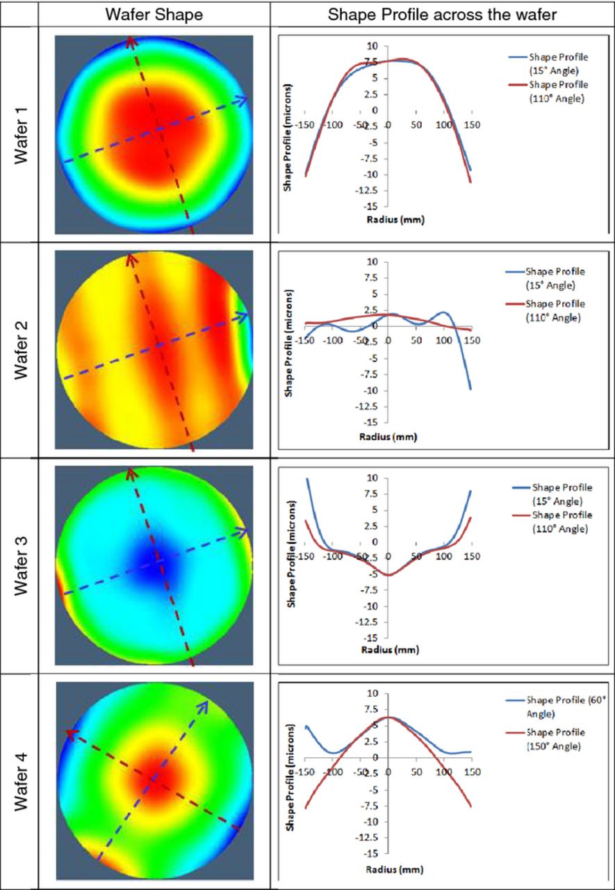
Figure 4. Diameter profiles across two different angular directions.
Thirdly, the traditional wafer shape metrics are defined by the median surface with gravitational sag corrected, In reality, the wafer is usually held horizontally with different chucking systems during wafer processing and therefore the influence of wafer gravity and chucking mechnisms cannot be igored since it has a significant impact to the overall wafer shape. Wafer in-situ shape during a process is determined by the interaction among the wafer gravity, the existing shape, the process tool chucking system, wafer temperature profile, and other factors. Figure 5 shows the 2D map of residual shape of the four wafers in response to two different chucking systems under wafer gravity effect. When the wafers are supported by 3 points near the wafer edges, the four wafers experience significant distortion at the center of each wafer. The shape of the wafers appear to be the same as it is dominated by low spatial frequency components due to gravitational effect. However, when the wafer is placed on a flat chuck, the global shape with low frequency signals is "damped" by wafer gravity and the residual shape of each wafer reflects its unique local shape variation (Table II).
Table II. Response of the four wafers on flat chuck and 3-pt chuck under gravity.
| Wafer # | Response on flat chuck (PV) | Response on 3-pt chuck (PV) |
|---|---|---|
| 1 | 2.2 μm | 143.7 μm |
| 2 | 4.5 μm | 143.4 μm |
| 3 | 8.5 μm | 144.1 μm |
| 4 | 2.8 μm | 143.8 μm |
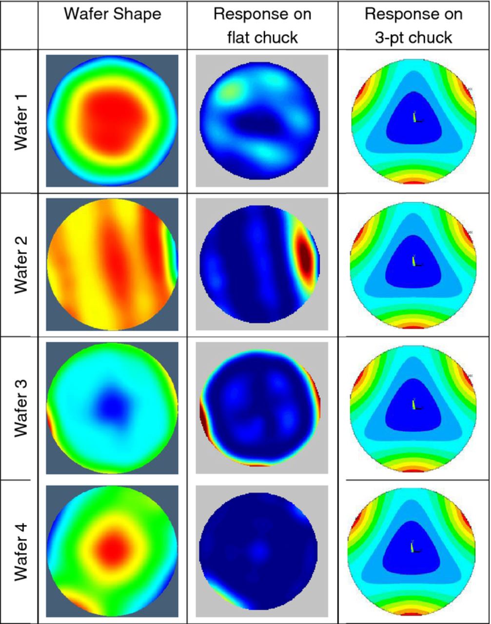
Figure 5. Response of the four wafers on a flat chuck and 3-pt chuck.
To address these limitations, several new global and local metrics are explored in this study (Figure 6).
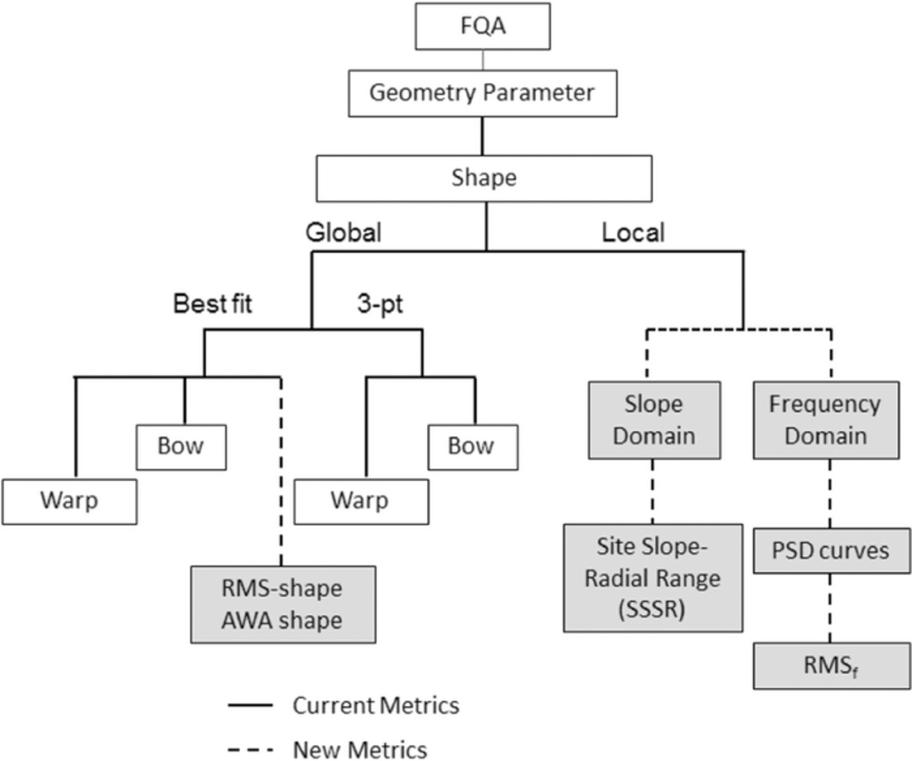
Figure 6. Flow chart of the current and new metrics explored in this study that quantify global and local characteristics of the wafer shape.
New Global Shape Metrics
To overcome some of the limitations of the traditional shape metrics, two new global metrics, RMS-shape and AWA-shape based on the averaging technique are explored. In this study, similar to the traditional shape metrics, the median surface of a wafer in a free and unclamped state is used. Unlike the traditional global shape metrics, however, the full median surface data are taken into consideration in these two metrics.
RMS-shape is defined as the square root of the sum of squares of mean deviation of each pixel with respect to a global least squares reference plane by Eq. 1. For computing AWA-shape a global least squares reference plane of wafer shape is established. Then the deviation of wafer shape with respect to the reference plan is computed. The wafer surface is then divided into grids of areas A1, A2, A3, AM. The absolute value of the mean deviation of wafer shape with respect to the reference plane within each grid is defined as X1, X2, X3, XM. Finally, the area weighted average of the absolute value of the mean deviation within each grid is defined as the AWA-shape metric (see Eq. 2).The basic concepts of these two metrics are demonstrated in Figure 7.
![Equation ([1])](https://content.cld.iop.org/journals/2162-8777/4/5/P155/revision1/jss_4_5_P155eqn1.jpg)
![Equation ([2])](https://content.cld.iop.org/journals/2162-8777/4/5/P155/revision1/jss_4_5_P155eqn2.jpg)
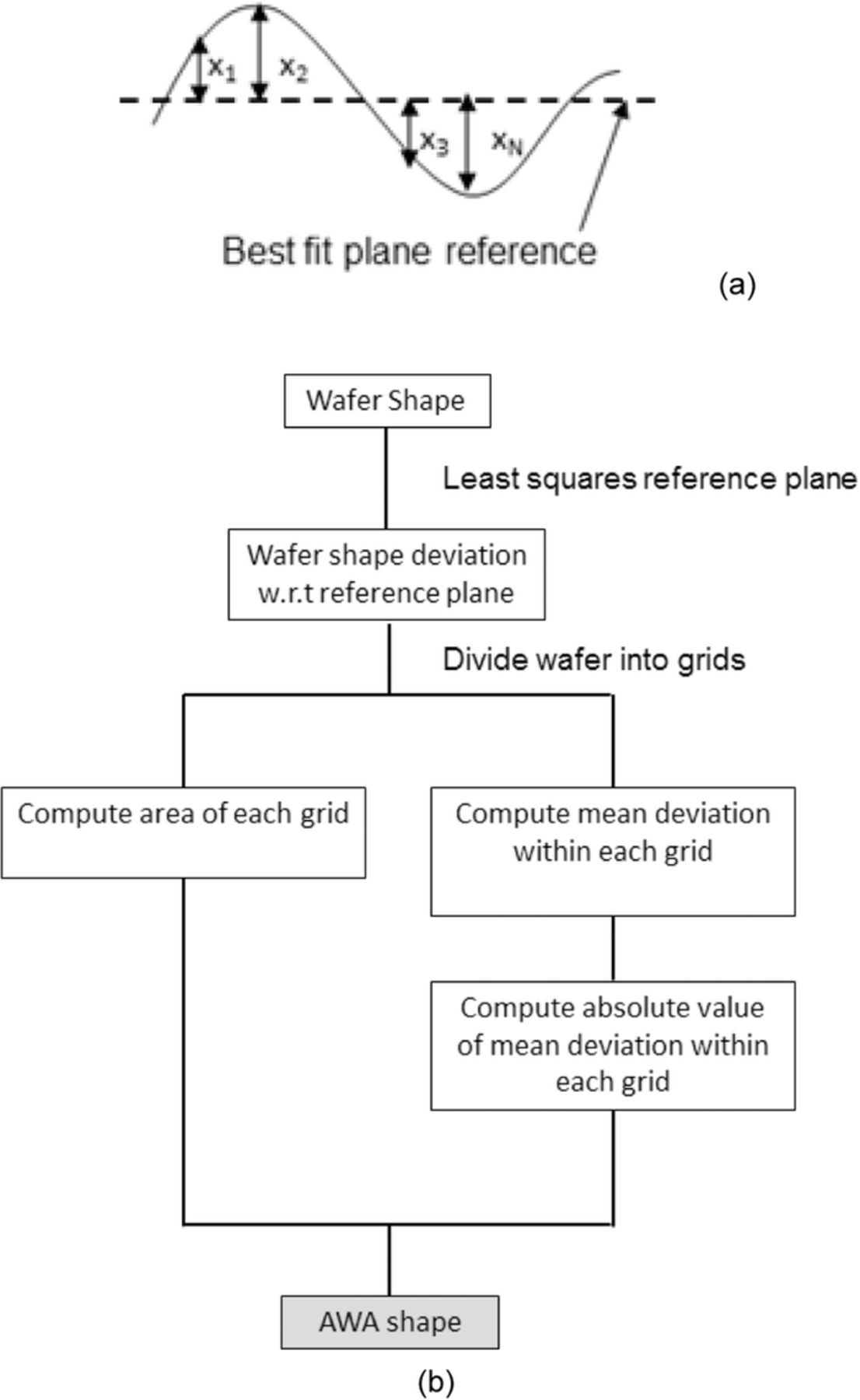
Figure 7. Concept of the global metrics (a) RMS-shape, and (b) AWA-shape.
Where x1, x2, x3, xN are deviation of wafer shape with respect to a reference plane, N is the total number of pixels on the wafer surface, A1, A2, A3, AM are the area of each grid, X1, X2, X3, XM are the absolute value of mean deviation of wafer shape within the grid.
The key advantage of RMS-shape and AWA-shape is that they both use full wafer median surface data instead only one center data point in Bow, or two data points at peak and valley used in Warp. The RMS-shape and AWA-shape metrics along with traditional metrics warp and bow for the four sample wafers are provided in Figure 8. Apparently, the two new metrics are following a similar trend between each other among the four wafers tested. However, they are trending differently from Warp-bf or Bow-bf. Compared to the other wafers, Wafer 2 has smaller RMS-shape and AWA-shape values. This is likely due to the sharp local shape variation near the wafer edge being averaged out by the global shape of the entire wafer. In addition, a very sharp local variation observed on Wafer 2 is likely attenuated more by AWA compared to RMS value since AWA-shape by definition is more sensitive to spatial grid and the weight for each grid (Figure 8). Inherited from the global shape definitions, the disadvantage of these new metrics, like the traditional shape metrics of Warp-bf and Bow-bf, are their inability either to capture or to predict the spatial locations of local shape variations on a wafer.
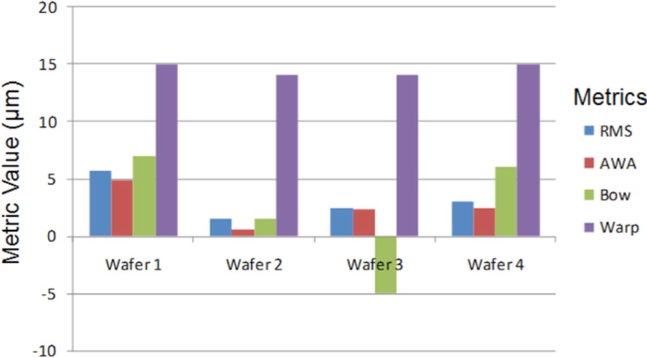
Figure 8. Comparison of traditional shape metrics, Bow-bf and Warp-bf, and new global shape metrics, RMS-shape and AWA-shape, of the four wafers.
Power Spectral Density Based Shape Metric
Traditional shape metrics as well as new RMS-shape and AWA-shape metrics are global shape metrics in the height domain and therefore cannot capture and quantify local shape variations on a wafer. The complex wafer shape contours shown in Figure 2 suggest that the wafer shape is composed of topographies with a wide range of spatial frequencies. In this study, one of the attempts is to analyze wafer shape in the frequency domain using well-established power spectral density (PSD) concept.20 One-dimensional PSD (1D-PSD) is used in the wafer shape analysis. Figure 6 shows a flow chart of the methodology applied.
In the computation, the entire wafer topography is divided into 360 sectors with 1 degree in each sector, and then the curve of 1D-PSD vs. spatial frequency for each sector can be obtained to reveal the wafer shape in each selected radial direction. A discrete 1D-PSD is a function of spatial resolution, topography value at each pixel, and the number of pixels, as shown in Eq. 3. The plot of 1D-PSD as a function of spatial frequency provides the topography characteristics of the wafer at each spatial frequency along the radial direction. The FRMS value at a frequency of interest can be obtained through discrete integration methodology by computing the area under the 1D-PSD curve bound by a narrow spatial frequency band with a mean frequency equal to the frequency of interest, as demonstrated in Eq. 4 and Figure 9. To illustrate if one has to compute FRMS at a spatial frequency of 10−3 μm−1 compute the area under PSD curve within the narrow spatial frequency band from 0.99 * 10−3 μm−1 to 1.01 * 10−3 μm−1.
![Equation ([3])](https://content.cld.iop.org/journals/2162-8777/4/5/P155/revision1/jss_4_5_P155eqn3.jpg)
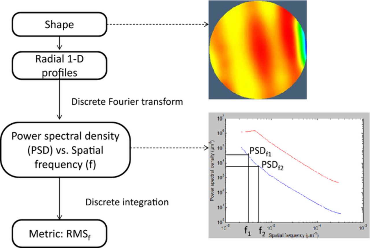
Figure 9. A flow chart of PSD-RMSf metric computation at a specific frequency band.
Where S1(fj) is the power spectral density (PSD), Δx is the spatial pixel resolution, zk is the z-value of topography at a pixel, N is the number of pixels on the 1D radial profile.
![Equation ([4])](https://content.cld.iop.org/journals/2162-8777/4/5/P155/revision1/jss_4_5_P155eqn4.jpg)
Where FRMS is the RMS value in height domain at the mean spatial frequency in the narrow spatial frequency band, f1 and f2 are the frequencies that define the spatial frequency band, PSDf1 and PSDf2 are the PSD values at spatial frequencies f1 and f2. Note: f1 and f2 are close to each other so that spatial frequency band is narrow.
To demonstrate the potential application of 1D-PSD in the frequency domain, the 1D-PSD concept is applied on the four wafers shown in Figure 2. Figure 10 shows the 1D-PSD curves in two radial directions A and B for all four wafers. As expected, the 1D-PSD curves for Wafer 1 in both A and B directions are very similar to each other since Wafer 1 has a simple global bow shape with no local shape variations. For Wafer 2, however, the 1D-PSD curve in the radial profile at 5 degree angle is much higher than that at 300 degree angle, clearly differentiating the local shape variations along these two radial directions. The kink observed in the 1D-PSD curve at 5 degree angle indicates a dominant spatial frequency of 0.00005 μm−1, which is the characteristic of its local shape variation. The FRMS value at the characteristic spatial frequency of 0.00005 μm−1 is computed using the equation 4 within a narrow spatial frequency band centered on the kink in the PSD curve at 5 degree angle. The FRMS value of other spatial frequencies can be easily calculated to capture a unique local shape feature or compare the angular shape differences, as demonstrated on Wafer 3 and Wafer 4 in Figure 10.
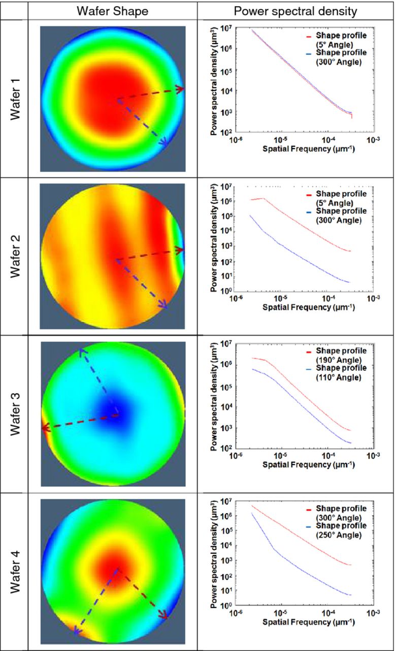
Figure 10. 1D-PSD curves at selected radial directions for the four wafers.
Site Based Local Shape Metrics
In this study, an attempt was made to characterize local shape variations in the slope domain. To quantify the local shape variations, a new site metric based on local shape change in the slope domain is developed. Figure 11 demonstrates a computation flow of one site based slope metric, Site Slope-Radial Range (SSRR). First, SSRR metric is starting from a wafer shape as defined in SEMI M59. Secondly, the x-slope and y-slope of the shape is computed at each pixel using the nearest neighbor shape data in the x-direction and the y-direction independently. Thirdly, the radial slope at each pixel is computed using the x-slope and the y-slope. Lastly, similarly to the site flatness calculation, such as SFQR, the customer defined site layout can be overlaid onto the radial slope map of a wafer. SSRR per each site can then be calculated by the range of the radial slopes of the pixels within of each site to quantify the local shape. In this paper, the traditional lithography exposure based layout with the site dimension of 26 mm × 8 mm is used for demonstrating the local shape concept.
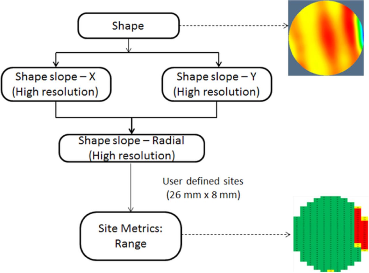
Figure 11. A computation flow of SSRR metric to capture sharp local slope change in a wafer.
To validate its effectiveness, the new metric is applied to the four wafers shown in Figure 2. The resulting SSRR maps in comparison with wafer shape maps are shown in Figure 12. To visualize the high slope regions on the wafer, two arbitrary cut-offs are applied to each color band for each wafer. The site-based shape slope radial range values increase from green to yellow to red. For wafers 1–3, the sites with SSRR less than 88 nm/mm are colored in green, the sites with SSRR greater than 88 nm/mm but less than 150 nm/mm are in yellow, and the sites with SSRR greater than 150 nm/mm are in red. For wafer 4, the site-based radial slope mean values are much smaller than that of wafers 1–3 due to different wafer processing. To capture the local shape variations on wafer 4, the sites with SSRR less than 65 nm/mm are colored in green, the sites with SSRR greater than 65 nm/mm but less than 100 nm/mm are in yellow, and the sites with SSRR greater than 100 nm/mm are in red. It is evident that the site-based shape slope radial range maps have relatively good correlation with the wafer shape maps. The sites with the highest radial slope mean values correctly flag the largest slope variation regions on a wafer shape map.
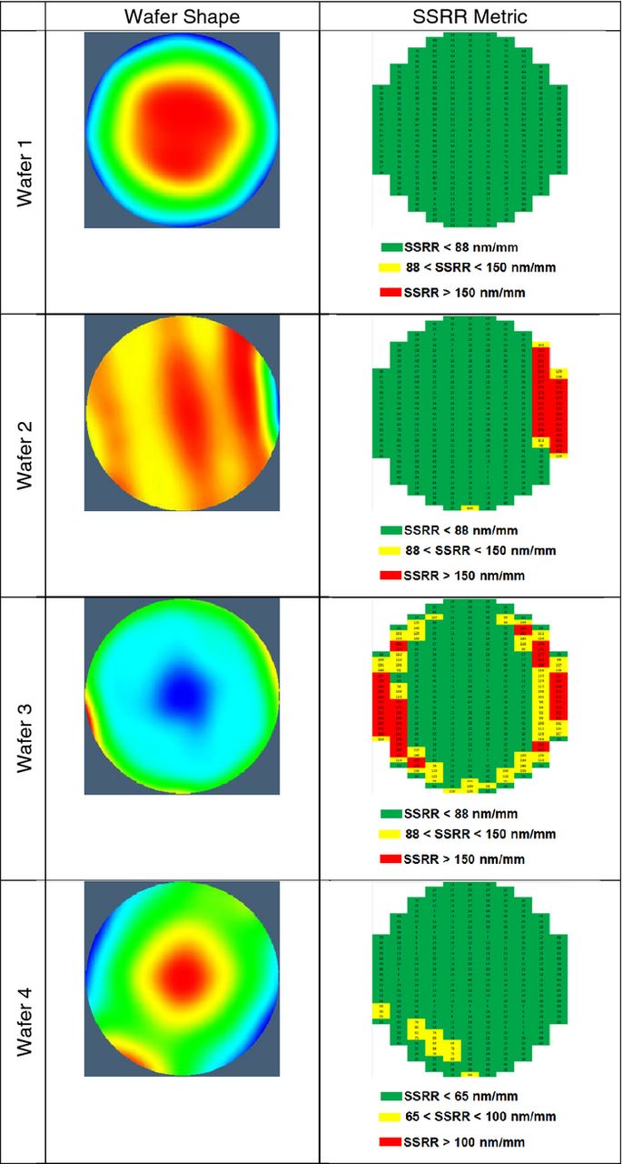
Figure 12. Wafer shape and SSRR maps of the four wafers.
Wafer 1 has a symmetric shape and hence has small SSRR values - less than 88 nm. This type of wafer may be good for traditional lithography application since large linear radial slope variations can be corrected by scanners, but it may impact CMP uniformity. Wafers 2 and 3 have large slope regions in the near edge region that can impact CMP and local lithography overlay performance.
Although the SSRR map can be calculated in the layout similar to the conventional site flatness metrics, such as SFQR or SBIR, the local wafer characteristics revealed by the slope metrics are fundamentally different. The conventional site flatness metrics are derived from thickness, while the slope metrics are from the wafer shape in the slope domain. Figure 13 clearly demonstrates the differences between site slope residual maps and site flatness maps, which confirms that site slope residual maps reveal unique wafer characteristics which cannot be captured by any existing site flatness and global shape metrics. To visualize the high SFQR regions on the wafer, the arbitrary cut-offs are used: the sites with SFQR less than 32 nm are colored in green, the sites with SFQR greater than 32 nm but less than 45 nm are in yellow, and the sites with SFQR greater than 45 nm are in red.
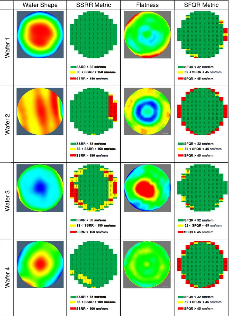
Figure 13. Comparison between the site-based shape slope metrics and the thickness-based SFQR flatness metric.
In this paper, only Site Slope-Radial Range is discussed. However, the site slope in X or Y direction may provide additional information to other applications. In addition to the range value, the other values may be useful, such as peak or mean. The site layout direction (either x-y or angular layout) and site dimension can be adjusted based on the applications.
Conclusions
Wafer shape is generally complex in nature and it consists of both global and local variations across the wafer. Traditional wafer shape metrics, Warp and Bow, are global metrics. Limited by their definitions, they cannot capture local shape variations that can be of interest for device manufacturing at advanced technology nodes. In addition, the two traditional metrics are oversimplified and therefore are not capable to quantify and rank the global wafer shape properly and consistently.
To address the shortcomings of traditional metrics, two new concepts of the global wafer shape, RMS-shape and AWA-shape, were developed in the height domain. These two new metrics utilize the full data of the median surface but two different averaging techniques. Based on the limited data analysis, these metrics are largely dominated by global shape components and no significant advantages were observed between each other.
To differentiate and quantify local shape variations, a novel approach is explored in this study. Wafer shape is composed of topography with a wide range of spatial frequencies. Based on this fundamental characteristic, 1D-PSD methodology was developed in the frequency domain. One of the outputs of this methodology is the 1D-PSD vs. spatial frequency curve. This curve captures unique shape characteristics in the frequency domain in response to the angular shape variations within a wafer. By comparing such curves at different angles within a wafer or of different wafers, the differences of local shape variations can be captured and compared. In addition, local shape variation at a specific frequency of interest can be quantified using RMSf. This new approach allows us to get comprehensive wafer shape information and will be beneficial to the wafer shape characterization. Further research and investigation is needed to take advantage of all information from PSD curve and provide guidance to minimize the local wafer variations in the silicon wafer development.
Driven by the need to control IC processes such as lithography and CMP process, a new site-based metric in the slope domain, SSRR, was developed. This metric captures local sites with large slope or sharp slope change on a wafer. This study has confirmed this new metric is not redundant to any existing site flatness or global shape metrics and can effectively capture unique local wafer shape variations in the slope domain. More investigation is in progress to validate the relevance of this new metric in lithography and other device manufacturing processes.