
Abstract
The increasing demand for portable and wearable electronics requires high reliability of devices for continuous miniaturization, and provides challenges for the dimensionally-confined bottom-up assembly methods which typically begin with materials such as graphene oxide (GO). However, GO based devices suffer from complicated synthesis procedures and lower device performance due to the presence of oxygen functionalities on the electrode materials, as well as the need to ensure a good interface between the electrode material and the electrolyte used. Here, a facile, two-step, top-down strategy was used to fabricate thin, all-in-one (PVA/H3PO4)/graphene/graphite paper-like electrodes. The assembled flexible, all-solid-state micro-supercapacitor devices exhibit excellent performance compared to previously reported values, such as a high volumetric capacitance of ∼3.6 F·cm−3 even after 20000 cycles. Notably, the devices also showed excellent rate performance with extremely high specific capacitance retention of up to 94% as the current density increased from 0.5 to 5 A·cm−3, indicating promise for high power applications. The paper-like electrodes were tailored to less than 0.5 mm width for further miniaturization and suffered from minimal capacitance attenuation. The excellent mechanical flexibility, capacity, and reliability indicate their promising application in energy storage devices.
Export citation and abstract BibTeX RIS

This is an open access article distributed under the terms of the Creative Commons Attribution 4.0 License (CC BY, http://creativecommons.org/licenses/by/4.0/), which permits unrestricted reuse of the work in any medium, provided the original work is properly cited.
The current development of portable electronics requires continuous miniaturization with low cost, while simultaneously enhancing the functionality and reliability of such devices.1 In the last decade, graphene has been isolated and identified as a superior candidate for electrode materials in energy storage devices to optimize their properties including flexibility, thickness, and weight.2,3 However, considering the compatibility and flexibility of on-chip integration, the performance of these electrodes typically deteriorates quickly with reducing size which urgently requires novel micro-fabrication techniques.4,5
A conventional supercapacitor typically consists of two electrodes, separated by an electrically insulating and ion conducting separator. The electrode is generally fabricated by casting of a slurry of active material combined with binders and conductive additives on a conductive substrate. The separator prevents electrical contact between the electrodes (i.e. short circuit), the binder immobilizes the active materials, the conductive additive improves the conductivity, and the substrate acts as the current collector. These additional components are mainly added to improve the performance of the active materials and have little contribution to its final capacitance. Therefore, many works in the literature artificially increase their measured capacitance by incorrectly using only the mass of the active materials instead of the true total mass of the electrodes (the total mass of each of these components).6–8
To address these issues, multiple strategies have been developed to simplify the micro-supercapacitor fabrication processes and avoid unnecessary components. For example, the interdigitated planar architecture becomes a better alternative to the conventional sandwich structure and avoids the need for the separator.4,6 Binder-free electrodes have been fabricated by growing the electroactive nanostructures directly on conductive substrates and successfully avoiding the additional binders and additives;10,11 Additionally, an all-in-one configuration was developed recently with no conductive additives, polymer binders and separators.12–14 These recently developed strategies not only simplified the process of device fabrication but also improved the utilization ratio and volumetric capacitance of the devices. However, there is still a long way toward higher practical performance and lower cost.
Here, we present a facile electrochemical exfoliation technique to produce a porous three-dimensional graphene surface structure. The in-situ exfoliation process promotes a good electrical connection between the active graphene layers and the graphite substrate. A novel solid state electrolyte infusion technique was carried out to assist the fabrication of paper-like electrodes for micro-supercapacitors. The thin paper-like electrode exhibited a sandwich hierarchical structure consisting of electrolyte (PVA/H3PO4)/graphene/graphite, with outstanding uniformity, mechanical flexibility, and superior conductivity. This hierarchically structured paper-like electrode can be directly cut into arbitrary shapes or sizes in accordance with specific requirements. Planar electric double layer capacitors (EDLC) were fabricated with different numbers of electrode fingers and widths and these exhibited excellent stability and electrochemical performance. Importantly, in this facile and novel strategy, the assembled solid-state supercapacitor devices are free from any separator, polymer binders, conductive additives, and metal-based current collectors.
Experimental
Electrochemical exfoliation of graphite
Commercial graphite foil (Gee graphite LTD, UK, 0.5 mm thickness and 25 mm width) was cut into strips 60 mm in length and used directly as the working electrode. The electrochemical process was carried out with a Pt mesh counter electrode and a DC power supply (BK PRECISION 1688B). The graphite foil was immersed into 0.1 M ammonium persulfate (APS, ≥98%, Aldrich) aqueous electrolyte and a constant voltage 10 V was applied for 5 minutes. Then, the foil was removed and washed with water and dried in a vacuum oven at 80°C overnight.
Fabrication of the electrode paper
The H3PO4/PVA gel electrolyte was prepared by mixing 1.0 g phosphoric acid (H3PO4, crystalline, ≥99.999%, Aldrich) and 1.0 g PVA (poly (vinyl alcohol), Mw = 89 000- 98000, 99+ % hydrolyzed, Aldrich) in 10 mL deionized water and then heated at 85°C for 1 h under vigorous stirring. Afterwards, ∼2.0 mL of H3PO4/PVA gel electrolyte was carefully drop-cast onto the exfoliated graphite foil and left standing overnight. Then, the H3PO4/PVA electrolyte film was peeled from the substrate leaving a coating of the exfoliated graphene and underlying graphite layers adhered to it. This hierarchical structure (consisting of the gel electrolyte and graphene coating) was used as the typical configuration of an all-solid-state supercapacitor electrode. The free standing solid-state electrode can be cut into arbitrary sizes in accordance with the requirements. Typically, the electrode film was measured to be ∼80 μm in thickness using a caliper.
Electrochemical measurements
All electrochemical tests were carried out on an Ivium B32160 electrochemical workstation (COMPACTSTAT.h, Ivium technologies). The electrochemical window for CV measurements and the galvanostatic charge-discharge tests was 0–0.8 V. The specific capacitances of the devices are calculated based on the following equations:

Or

Where I is the applied working current, Δt represents the discharging time, Δ V = V2-V1 represent the potential window. v is the scan rate of the CV curve. d is the total volume of the active materials in two electrodes.
Characterization
The morphology of the paper-like thin film was characterized using both a scanning electron microscope (SEM, Philips XL30 FEGSEM) and transmission electron microscope (TEM, Philips CM20). FTIR (Fourier Transform Infra-Red) Spectroscopy was used to determine the chemical functional groups of the sample. X-ray photoelectron spectroscopy (XPS) was performed with a Kratos Axis Ultra X-ray photoelectron spectrometer; the curve fitting was accomplished by CasaXPS software. Sheet resistance was measured using a four-point probe and source-measure unit (Keithley 2400).
Results and Discussion
Structural characterization of the electrode paper
Electrochemical exfoliation has been previously exploited as an effective and facile strategy to produce large quantities of graphene flakes. Various salt solutions have been utilized as the electrolyte, including both aqueous solutions (e.g., K2SO4 and (NH4)2SO4)15 and organic solvent based systems (lithium salts16 or perchlorate salts).17 As shown in Figure 1, in this work we use aqueous APS solution as the electrolyte for electrochemical exfoliation, which has been demonstrated to be another effective electrolyte. This can be attributed to the synergy between the hydroxyl and sulfate radicals. The hydrolysis of persulfate occurs which produces sulfate radicals. Hydroxyl and oxygen radicals come from the electrolysis of the water and will facilitate the intercalation of sulfate radicals into the space between the graphite layers and curl the edge of the layers. Sulfate ions expand the interlayer spacing and provide access for further radicals. As shown in step I, completely exfoliated graphene layers are removed while curled; partly exfoliated layers are adhered to the graphite, and form a roughened and porous surface. Then, in step III, the electrode paper can be easily peeled off after the gel electrolyte (PVA/H3PO4) was carefully drop-cast (step II) and left to solidify overnight. The PVA/H3PO4 gel permeated into the porous stacked graphene and interconnected the graphite substrate and graphene layers, not only acting as an adhesive to separate from the substrate but also working as the electrolyte. Then, the micro-supercapacitor device was fabricated by cutting the electrolyte/graphene/graphite paper into the desired pattern and drop-casting additional electrolyte gel between the two electrodes.
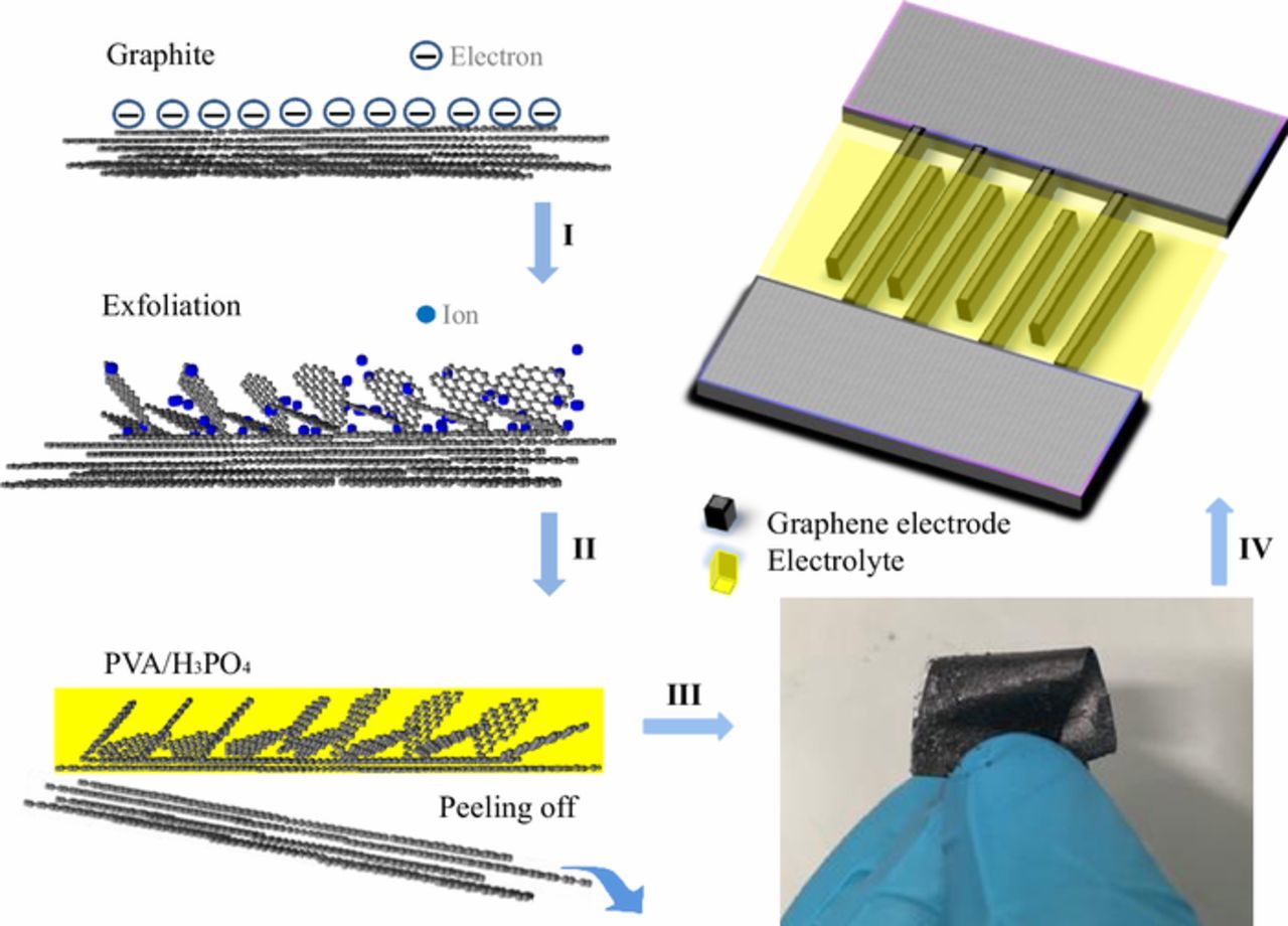
Figure 1. Schematic showing the process of micro-supercapacitors preparation (I-IV): I) electrochemical exfoliation of graphite foil; II) coating the graphene/graphite foil with gel electrolyte (PVA/H3PO4); III) peeling off the flexible graphene paper-like electrode; IV) fabrication of the interdigitated micro-supercapacitor devices using the electrode paper.
SEM analysis was performed before and after drop-casting the gel electrolyte. As shown in Figures 2a and 2b, the expanded graphene layers possess an interconnected porous network with most of its pores having a size of several micrometers. The increased magnification image in Figure 2b presents the typical interconnection between the different layers, graphite was expanded into thin graphene layers and formed the pores while the π-conjugation between unexploited graphite layers maintains cross-linking with each other and the graphite substrate. Thus, the electrolyte can easily permeate into the pores between layers and even connect with the graphite substrate. The cross section SEM image in Figure 2c demonstrates the hierarchical structure of the paper-like electrode. There is a visible difference in the morphology of the disordered porous graphene layers and the stacked graphite layers, and the thickness of the active material layer can be identified to be approximately 20 μm, while it is ∼30 to 60 μm for the graphite substrate and this depends on further polishing. Typically, the electrode paper used for the device assembly had a total thickness (including substrate, graphene layer and solid-state electrolyte layer) of ∼80 um, as measured by a micro caliper and SEM.
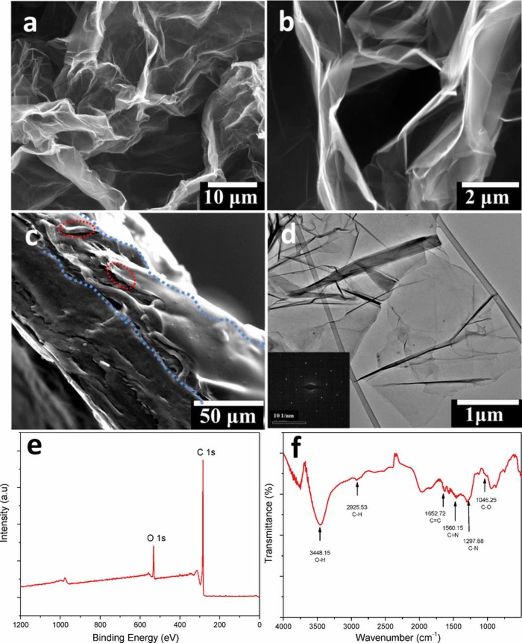
Figure 2. (a-b) SEM images of the exfoliated graphene electrode with different magnifications. (c) Cross section image of electrode paper observed by SEM (the blue lines indicate the boundary of the hierarchical structure and the red circles show the contact interface between graphene and PVA/H3PO4 electrolyte). (d) TEM image of a detached graphene flake (inset is the SAED pattern of the flake, the scale bar is 10 1/nm). (e) XPS spectrum of the exfoliated graphene. (f) FTIR spectrum of the exfoliated graphene.
TEM analysis was carried out on one of the detached graphene flakes as shown in Figure 2d to further verify the quality of the exfoliated layers, and reveals that the graphene sheets are typically few layers in thickness. The inset selected area electron diffraction (SAED) image with the typical 6-fold symmetry illustrates the expected crystalline structure of the graphene layers.18 XPS analysis (Figure 2e) and FT-IR spectroscopy (Figure 2f) were also applied to examine the composition of the electrochemically exfoliated graphene. Despite the oxidation process occurring during the electrochemical exfoliation, only a small amount of oxygen doping was detected and the molar ratio of C:O was calculated to be 17.5 (Figure 2e). This value is significantly lower oxygen content than those previously reported for reduced graphene oxide (rGO) or even exfoliated graphene,15,19 indicating the high quality and pristine nature of the exfoliated material. Analysis of oxygen functionalities was further determined by the FTIR analysis (Figure 2f) and the majority of functional groups are C-OH or C-O groups which originate from reactions with water.
The electrochemical exfoliation process ensures the close integration of the layers of active material with the current collector, allowing for low contact resistance and good mechanical flexibility. As shown in Figure 3, the good flexibility and processability enable arbitrary design of the electrode paper. For example, electrode fingers with uniform size have been tailored and assembled to form 2, 4, and 6 finger supercapacitors (as shown in Figures 3c, 3d, and 3e respectively) to test their performance and reliability for on-chip integration in practical devices. The flexibility of the electrodes enables it to wrap around a pencil (Figure 3a) or adhere to fabric (Figure 3d), indicating the versatility of this paper-like gel electrode. Also, rectangular electrodes with the sizes of 1.0 mm (width) × 8.0 mm (length) and 1.0 mm × 0.5 mm have also been achieved (Figure 3f), indicating the excellent machinability of the electrode paper. Resistance measurements obtained using a four-point probe revealed that the thin electrode paper still maintains a low sheet resistance of ∼0.24 Ω/□ on the underside. The electrochemical performance of the different micro-supercapacitor devices is shown in the cyclic voltammograms (CV) in Figures 3g, 3h and 3i (corresponding to the devices in Figures 3c, 3d and 3f), and their quasi-rectangular shape at a scan rate of 100 mV·s−1, indicates an ideal electric double-layer capacitive behavior. With increasing number of fingers or changing of their architecture, there is little shape variation of the CV response.
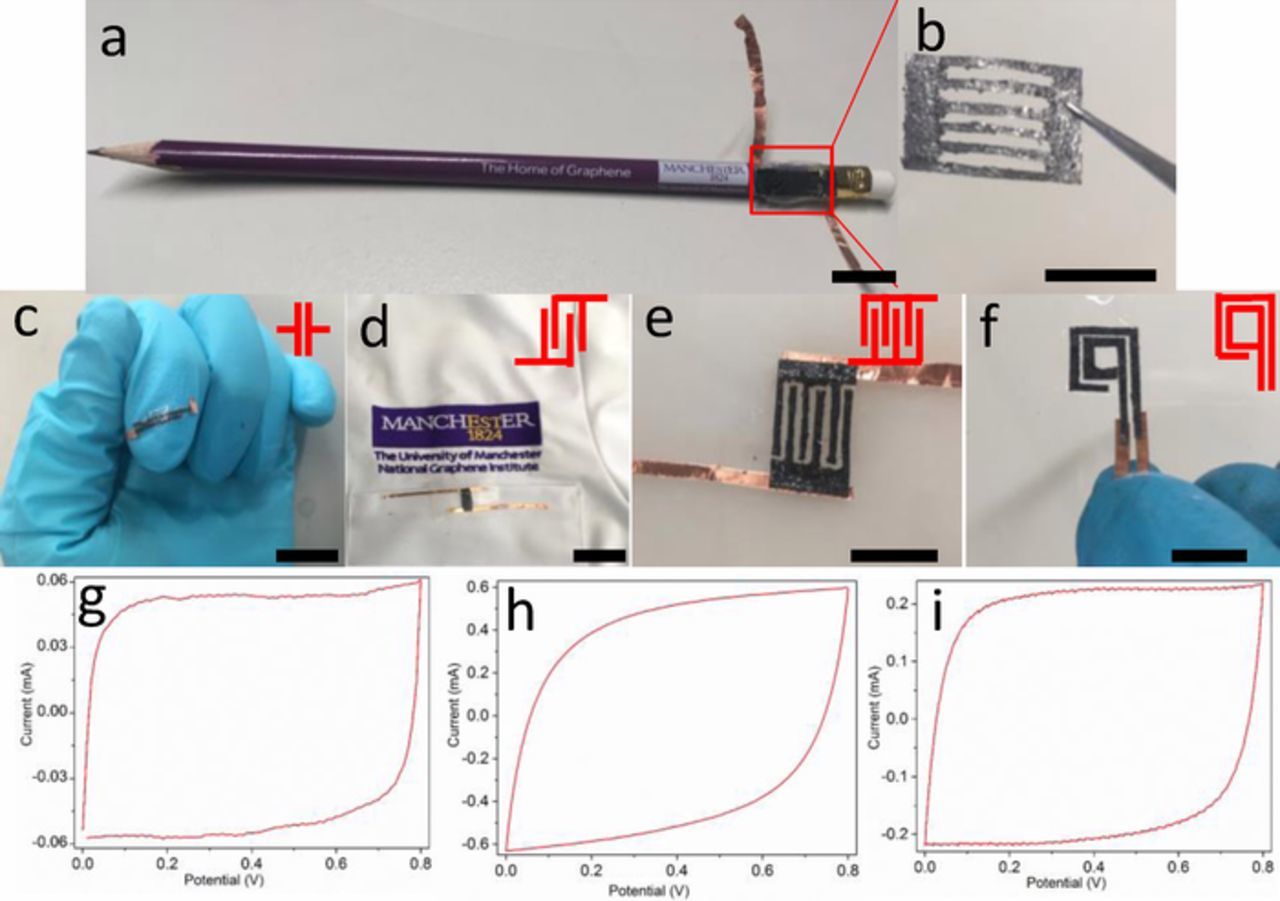
Figure 3. Optical photographs of micro-supercapacitor devices; wrapped around a graphite pencil (a), image of the patterned paper-like electrode (b), a device on a finger (c), and adhered on fabric (lab coat) (d). Photographs of micro-supercapacitors with 2, 4 and 6 interdigitated fingers, (c), (d) and (e) respectively. Photograph of a square shaped supercapacitor (f). (Scale bar: 1 cm for each image). CV response of the supercapacitor devices (scan rate: 100 mV·s−1) for the two finger supercapacitor (g), four finger supercapacitor (h), and the square shaped supercapacitor (i).
Mechanical flexibility of the supercapacitor devices
Characterization of the mechanical flexibility of the graphene based solid-state supercapacitor devices was carried out to evaluate their functionality and reliability. As show in Figure 4a, when bending the device to different angles of 0°, 90°, or 180°, the CV curves of the device exhibited almost identical quasi-rectangular shapes at a scan rate of 200 mV·s−1, demonstrating the mechanical robustness and flexibility of the electrode paper. Unlike traditionally-used copper or nickel-based electrodes, the in-situ produced graphene layers ensure a uniform contact with the graphite substrate and do not delaminate, fracture and fall off even with structural distortion. This is vital for use in applications such as flexible wearable electronic devices.
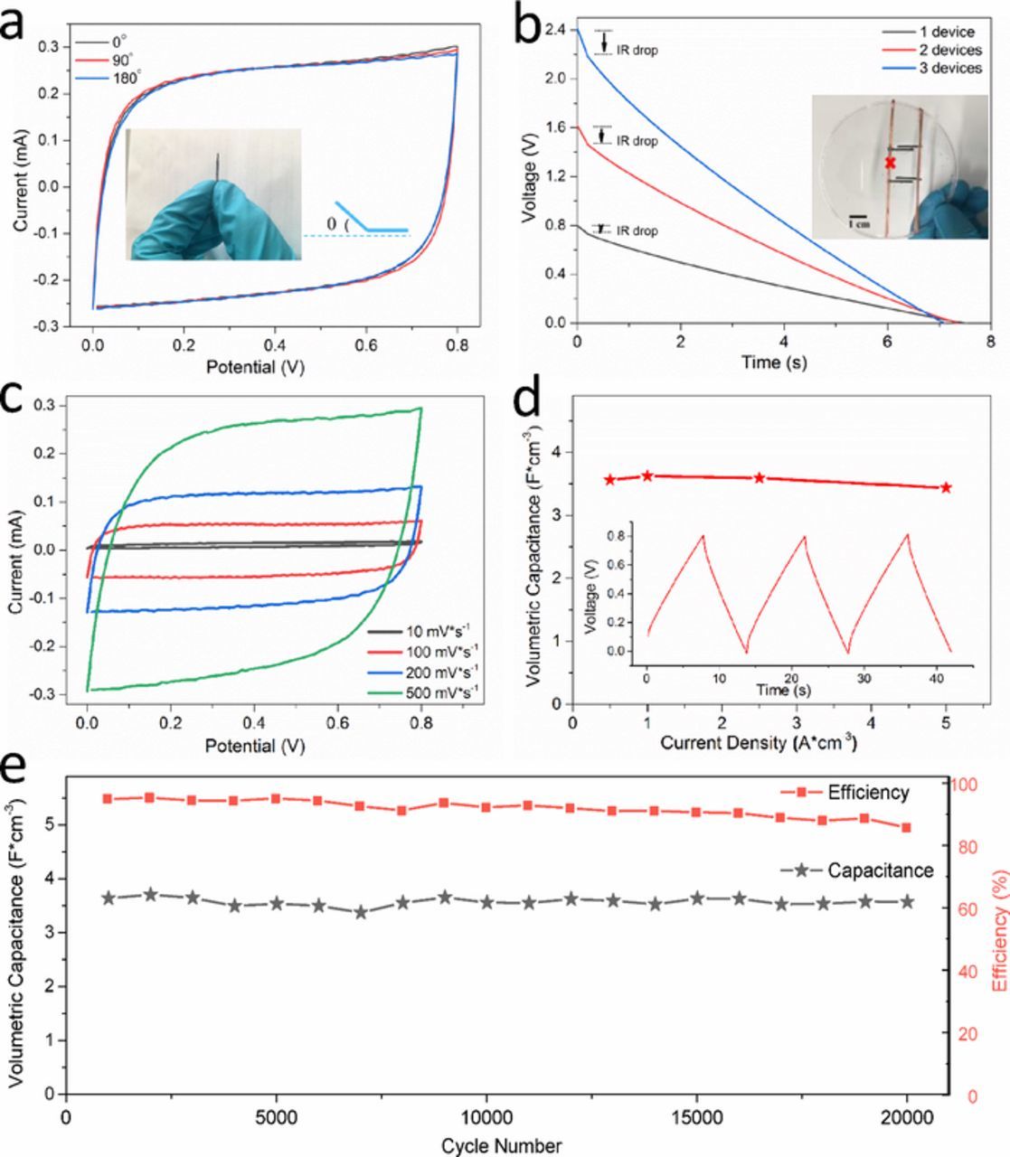
Figure 4. Electrochemical performance of the supercapacitor devices (electrode: 0.5 mm × 1 cm). (a) CV curves with different bending angles as labelled (scan rate: 200 mV·s−1); (b) discharge curves of single, double, and triple devices connected in series (current density: 1 A·cm−3) (inset is the optical image of two parallel devices); (c) CV curves of one single device with increasing scan rates; (d) specific capacitance of the device (inset is the charge-discharge curve at 1 A·cm−3); (e) cycling performance of a single device at 2 A·cm−3 and corresponding coulombic efficiency.
Scalable integration of the devices
The paper-like electrodes can also be assembled in series (or parallel) to better replicate real-world usage for practical applications. As shown in the inset of Figure 4b, uniformly sized parallel electrodes of 1 mm width were shaped by razor. Here, 1 to 3 serially-connected devices have been fabricated to compare their performance with a stepwise voltage increase from 0.8, 1.6 to 2.4 V. Their galvanostatic charge and discharge profiles were measured at 1 A·cm−3. The nearly linear discharge curves and roughly equal discharge times demonstrate their consistent performance. Low IR drops were observed with each device, again demonstrating the good conductivity of the integrated electrode paper. Furthermore, dependence of the electrochemical performance on the electrode size is also seen as one of the key factors that contributed to their performance consistency and reliability with continuous miniaturization. The free standing solid-state electrode films were cut into arbitrary sizes in accordance to the requirements as shown in Figure 3 and showed excellent machinability and stability. Therefore, the interdigitated electrodes were further miniaturized and patterned with a planar width of ∼0.5 mm. Figure 4c shows the CV behavior at different scan rates from 10 to 500 mV·s−1, the quasi-rectangle shapes were observed and indicates its ideal electric double-layer capacitive behavior. The volumetric capacitance of the device was calculated to be ∼5.2 F·cm−3 at scan rate of 200 mV·s−1. Furthermore, the volumetric capacitance of the device with different electrode width was also calculated and only a minor fluctuation was observed, which shows promise for further miniaturization.
Cycle performance
Cyclic voltammetry allows us to understand the electron transfer kinetics and the reversibility of the device cycles, while galvanostatic charge-discharge (GCD) measurements evaluate their practical application performance. The volumetric capacitance is recognized to be a more reliable parameter than the gravimetric parameter for evaluating the practical performance of such small scale micro-supercapacitor devices.20 Therefore, the volumetric capacitance of the device was calculated from the GCD curves over a wide range of charge/discharge current densities from 0.5 to 5 A·cm−3. As shown in Figure 4d, the supercapacitor device achieved a volumetric capacitance of ∼3.6, ∼3.6, ∼3.6 and ∼3.4 F·cm−3 at current densities of 0.5, 1, 2.5 and 5 A·cm−3, respectively. The high capacitance retention with increasing current density indicates the high power performance of this device architecture. The inset in Figure 4d further shows the GCD curves at 1 A·cm−3, the linear symmetric curves indicate ideal double-layer capacitive behavior. Furthermore, Figure 4e shows the cycling performance with more than 20000 cycles under a high current density of 2 A·cm−3. The device exhibited a stable cycle life between 0 and 0.8 V and remained about 98% of the initial capacitance after 20000 charge-discharge cycles. Simultaneously, the device maintains its coulombic efficiency up to 86% after extended cycling, this decrease is attributed to the gradual dehydration of the solid-state electrolyte which was not encapsulated during the testing. The high rate performance and cycle stability are attributed to the integrated structure of the multi-component electrode paper, such as the interface between the active materials (graphene) and current collector (graphite). This structure provides an ideal path for ionic and electron transport, as the porous graphene layer is well connected with permeated electrolyte and possesses a high surface area, resulting in a low interfacial resistance and high capacity.
In order to evaluate the relative performance of the device architecture, a plot of volumetric capacitance for different solid-state supercapacitor materials and designs from the literature is shown in Figure 5. The plot shows that our device achieved a considerably higher capacitance and remarkable rate performance. For instance, when the current density increased from 0.5 to 5 A·cm−3, the device showed high specific capacitance retention of up to 94%, which is higher than all the works referred here. Comparing the volumetric capacitances under the same current density, our solid-state device demonstrates superior performance compared to those previously reported for similar nanocarbon/polymer systems.21–26

Figure 5. Rate performance plot of our device compared with similar reported carbon/polymer supercapacitor devices.
Conclusions
We have demonstrated here an electrochemical exfoliation process to directly fabricate a graphene paper-like electrode for solid-state energy storage applications. A novel strategy was applied to protect and peel off the thin graphene-based electrode using a solid-state gel electrolyte. The thin (∼80 μm) and well-ordered electrolyte/graphene/substrate sandwich exhibited remarkable conductivity (∼3.9 Ω·cm−1) and excellent mechanical flexibility, which suggests promise for further miniaturization. Furthermore, micro-supercapacitor devices were fabricated and a high volumetric capacitance of ∼3.6 F·cm−3 was achieved at a current density of 2.5 A·cm−3. With increasing current density these solid-state devices retained 94% of their capacitance value and this can be attributed to the excellent interface between the porous graphene layers and the gel electrolyte. With high capacitance (∼3.6 F·cm−3), long cycle performance (20000 cycles), high rate capability (94%), and simple and additive free construction, this facile scalable integration of planar devices opens up a new route for the continuous miniaturization progress of graphene-based energy storage devices.
ORCID
Alexander J. Marsden 0000-0002-3017-1754
Zheling Li 0000-0001-8412-0234
Mark A. Bissett 0000-0002-8908-7960