
Abstract
Cu(111) preferential orientation is desired to improve the electromigration resistance in Si-LSI (LSI) and 3D-LSI. In this study, we examine the orientation and grain size of a Cu film in a Cu/TaWN/SiO2/Si system by using a 5 nm thick TaWN alloy film that functions as both a thin diffusion barrier and underlying material that induces preferential Cu(111) orientation. The Cu film with highly-oriented growth of Cu(111) and an average grain size of ∼160 nm was obtained on the as-deposited TaWN (5 nm thick)/SiO2/Si system. The Cu/TaWN/SiO2/Si system tolerates annealing at 700 °C for 60 min without Cu diffusion and/or configurational change.
Export citation and abstract BibTeX RIS
In Si-LSI (LSI) and 3D-LSI, significant miniaturization of the Cu interconnect has continued to progress, 1–6) where reduction of the interconnect resistance and improvement of the electromigration (EM) resistance are strongly required. 7) Under these circumstances, the realization of Cu(111) orientation, which is the most resistant to EM, is strongly desired. 8,9) The Cu interconnect is usually obtained by depositing a Cu seed film on a diffusion barrier by PVD, CVD, or ALD, followed by depositing a plated Cu film. 10) By obtaining a Cu seed film with Cu(111) orientation, the subsequent plated Cu film can also grow on the (111) plane. 11) A large grain size and (111) orientation of the Cu film are generally important for improving the EM resistance. However, diffusion barriers and underlying materials, such as Ta/TaN and Ta/TaN/Ta, which form bilayer or trilayer structures, are used to obtain Cu(111) orientation. 12,13) This reduces the cross-sectional area of the Cu interconnect, resulting in the secondary problem of increased interconnect resistance. Therefore, developing a material that functions as both a thin diffusion barrier and an underlying material that preferentially induces orientation of the Cu(111) plane is desired; however, to the best of our knowledge, no such material has been reported so far. On the other hand, we proposed TaWN alloy films with the above two functions in our previous study, 14) and we demonstrated that the 5 nm thick TaWN alloy film is an excellent barrier in the Cu/TaWN/Si system, which effectively suppresses Cu diffusion. 14–16) Furthermore, we demonstrated that a Cu film with a high orientation of Cu(111) on the TaWN/Si system can be obtained using only a 5 nm thick TaWN alloy film without the need for an underlying material for Cu orientation. 16)
In ADMETA2022, we reported formation of the Cu film with Cu(111) orientation on the TaWN/SiO2/Si system using X-ray diffraction (XRD) and ω-rocking curve measurements. 17) In this study, we investigate whether highly-(111) oriented and large-grained Cu films can be obtained on the TaWN/SiO2/Si system using a 5 nm thick TaWN alloy film. Details of the orientation and grain size of the Cu films on the TaWN/SiO2/Si system employing a 5 nm thick TaWN alloy film were added new data by scanning electron microscopy with electron back-scatter diffraction (SEM-EBSD) analysis.
The Cu/TaWN/SiO2/Si systems were prepared using a tetrode dc sputtering system. A thermally oxidized SiO2/Si wafer was used as the substrate. After evacuating the sputtering system to a base pressure of 5 × 10⁻⁷ Torr, the 5 nm thick TaWN alloy film was deposited on the SiO2/Si substrate by reactive sputtering of a Ta–W (99.99%) composite target using a Ar+N2 (40%) gas mixture, at a substrate temperature of 400 °C. The Cu film (150 nm) was then sputter-deposited onto the TaWN alloy film using Ar gas at RT without breaking the vacuum. The sputtering gas pressure in each deposition was 2 × 10⁻³ Torr, and the target voltage and current for TaWN deposition were 1 kV and 80 mA, respectively, while those for Cu deposition were 500 V and 80 mA, respectively. Notably, the sputtering conditions and film thickness of the TaWN alloy film and Cu film were the same as the sputtering conditions and film thickness in our previous study. 14,16) Some of the specimens were annealed at various temperatures for 1 h under a vacuum of 10−7 Torr. The heating and cooling rates of the vacuum annealing equipment were both set to 10 °C min−1. XRD (θ–2θ scan), ω-rocking curve measurements, and SEM-EBSD were used to evaluate the crystallography and texture of the specimens.
Figure 1 shows the XRD patterns of the Cu/TaWN/SiO2/Si system employing a 5 nm thick TaWN alloy film before and after annealing at 500 °C and 700 °C for 1 h. In Fig. 1(a), only very high intensity peak of the Cu(111) plane were observed. A very weak and broad pattern around 35° was also observed, in which the peak was shifted toward lower 2θ value than that (35.83°) of fcc-TaN(111). 18) Considering this peak shift, it seems that the TaWN alloy lattice expands. While the Cu(200) diffraction peak was observed for the as-deposited Cu/TaWN/Si system, 16) no peak of the Cu(200) plane was observed for the as-deposited Cu/TaWN/SiO2/Si system. Moreover, as evident from Figs. 1(a) and 1(b), the peak of the Cu(111) plane became more intense with increasing annealing temperature. On the other hand, annealing at 700 °C did not induce the formation of new reaction products such as Cu silicides in this system.
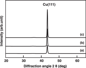
Fig. 1. XRD patterns of Cu/TaWN/SiO2/Si system using a 5 nm thick TaWN alloy film: (a) before annealing, (b) after annealing at 500 °C, and (c) after annealing at 700 °C for 1 h.
Download figure:
Standard image High-resolution imageFigure 2 shows ω-rocking curves of Cu(111) peak from the Cu/TaWN/SiO2/Si system using a 5 nm thick TaWN alloy film before and after annealing at 500 °C and 700 °C for 1 h. This is a direct measure of the angular distribution of the mosaic texture along the direction of the substrate normal. FWHM values of the Cu(111) pattern in Fig. 2 were 3.45° before annealing, 3.11° and 2.36° after annealing at 500 °C and 700 °C, respectively. In our previous study, FWHM values of the Cu(111) pattern for the Cu/TaWN/Si system were found to be 5.86° before annealing, 4.68° and 4.73° after annealing at 500 °C and 700 °C, respectively. 14) The degree of Cu(111) orientation in this system was found to be higher than that in the Cu/TaWN/Si system.
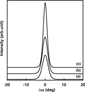
Fig. 2. ω-rocking curve measurement of the Cu(111) peak obtained from Cu/TaWN/SiO2/Si system using a 5 nm thick TaWN alloy film: (a) before annealing, (b) after annealing at 500 °C, and (c) after annealing at 700 °C for 1 h.
Download figure:
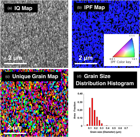
Standard image High-resolution imageThe orientation and grain size of the obtained Cu film in the as-deposited Cu/TaWN/SiO2/Si system were investigated by SEM-EBSD. Figures 3(a)–3(d) shows the image quality map (IQ map), inverse pole figure map (IPF map) in the normal direction (ND), unique grain map, and grain size distribution histogram of the Cu(111) reflections from the as-deposited Cu/TaWN/SiO2/Si, respectively. In Fig. 3(a), there are more bright areas than dark areas, indicating that EBSD patterns are detected in the large area. Therefore, the crystal orientation and grain size of Cu film can be evaluated using EBSD. In Fig. 3(b), the orientation perpendicular to the specimen surface is colored through the unit triangle. Cu(111) mainly appears in blue and dark colors. Dark areas are often seen when cutting unreliable areas.
Fig. 3. EBSD analysis of the Cu(111) reflections obtained from as-deposited Cu/TaWN/SiO2/Si system using a 5 nm thick TaWN alloy film: (a) IQ map, (b) IPF map (ND), (c) unique grain map, and (d) grain size distribution histogram.
Download figure:
Standard image High-resolution image
The IPF map of the as-deposited Cu film shows primarily (111) orientation in the thickness direction [Fig. 3(b)]. Figures 3(c) and 3(d) show the grain size distribution of the Cu film on the TaWN alloy film. The average grain size of the Cu film on the TaWN/SiO2/Si system calculated from this grain size distribution is approximately 160 nm, which is almost the same as the Cu film thickness. In contrast, the average grain size of the Cu film on the TaWN/Si system was approximately 90 nm. Cu/TaWN bilayer deposited on the SiO2/Si and Si substrates were formed under the same sputtering conditions and film thickness, but there were differences in the orientation and grain size of the Cu film. These results suggest that the orientation and grain size of the Cu films are related to differences in orientation, film morphology, or roughness of the TaWN alloy film on SiO2/Si and Si substrates.
In conclusion, we investigated the orientation and grain size of a Cu film on a TaWN/SiO2/Si system employing a 5 nm thick TaWN alloy film. The obtained data demonstrate that a relatively large grain size and preferential Cu(111) orientation can be realized not only on Si substrates, but also on SiO2/Si substrates. These results demonstrate that the TaWN alloy film is an excellent material that functions as both a diffusion barrier and as an underlying material for controlling the Cu(111) orientation. Pan et al. reported that a Cu film deposited on a 25 nm thick Cu seed film with Cu(111) orientation is dominant (111) orientation. 11) Since similar results are expected in this study, the obtained Cu film is a possibility as a thin Cu seed film with its large crystal grain size and preferential (111) orientation. We are currently investigating the factors responsible for these favorable properties, but they are inconsistent with previous theories of surface energy and strain energy. The orientation mechanism will be discussed in the near future.
Acknowledgments
Part of this study was supported by JSPS KAKENHI Grant No. 21K04150.