
Abstract
The discussion in Chap. 4 showed that the four basic converter topologies have their output conversions determined by the duty ratio, D, and that they consist of a single input and a single output with a common reference point. For applications in which the output voltage does not differ from the input voltage by a large factor, those topologies can be used. However, for many applications, the input voltage is normally derived from an off-line half- or full-wave rectifier, and the output voltage is normally a very small fraction of the rectified dc input voltage. As a result, transformers must be added between the power stage and the output for the purpose of voltage scaling. Unlike line-frequency transformers, these transformers are high frequency and much smaller in size and weight. In addition, transformers are used in switching mode converters for electrical isolation between the input and output; reduction of stresses in switching devices; and provision multi-output connections. With isolation transformers, the output voltage polarity reversal does not become a design restriction. Also in some application, system isolation may be required by the certain regulatory body. However, the benefits obtained by adding isolation transformers come with a price. The major drawbacks include high converter volume and weight, reduced efficiency, and added circuit complexity to limit the effect of leakage inductance and avoid core saturation.
Author information
Authors and Affiliations
Problems
Problems
5.1.1 Forward Converter
-
5.1
Consider the single-ended forward converter of Fig. P5.1 by including a leakage inductance of the power transformer. Discuss the effect of L k on the circuit operation.
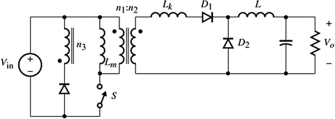
Fig. P5.1
-
D5.2
Design a forward converter of Fig. 5.11 that needs to supply 400 W at 15 A load current. The output ripple should not exceed 1%.
-
5.3
Derive the expression for the output ripple voltage for a forward converter of Fig. 5.11.
-
5.4
The circuit given in Fig. P5.4 is another type of a forward converter. Sketch the primary voltage and diode currents waveforms for the circuit.
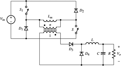
Fig. P5.4
-
5.5
Replace D 1 and D 2 by S 3 and S 4, respectively, in Problem 5.45. Derive the voltage gain if the four switches have the switching waveform in Fig. P5.5.
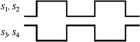
Fig. P5.5
-
5.6
Consider the single-ended forward converter given in Fig. P5.6 that uses a regular and a Zener diode to provide a negative voltage damp across the primary in order to reset the core to avoid transformer saturation. (a) Discuss the operation of the circuit, and (b) sketch the current waveform \( {i}_{{\mathrm{D}}_1}, \) \( {i}_{{\mathrm{D}}_2}, \) i L, \( {i}_{{\mathrm{D}}_3}, \) i sw, and i D.
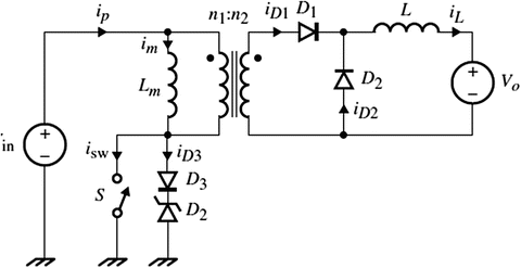
Fig. P5.6


5.1.2 Full-Bridge
-
D5.7
Design the full-bridge dc-dc converter with a center-tap output transformer with the following specifications: V in = 480 V, V o = 240 V at I o = 20 A, and f s = 75 kHz.
-
5.8
Sketch the labeled current and voltage waveforms for the double-ended buck-derived converter shown in Fig. P5.9. Assume the switching sequence for S 1 − S 3 and S 2 − S 4 is the same as that in Fig. 5.18b. Assume RC ≫ T.
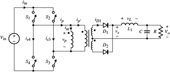
Fig. P5.8
-
5.9
Repeat Example 5.6 by using the switching sequence in Fig. P5.10. Derive the voltage gain in terms of the phase shift period D 1.
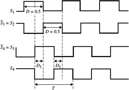
Fig. P5.9


5.1.3 Push-Pull Converter
-
5.10
Derive the output voltage ripple for the push-pull converter.
5.1.4 Isolated SEPIC Converter
-
5.11
Derive the voltage gain equation for the isolated SEPIC converter shown in Fig. P5.11.
Fig. P5.11
-
5.12
Derive the voltage gain expression for the isolated Cuk converter shown in Fig. P5.12.
Fig. P5.12


5.1.5 Weinberg Converter
-
5.13
Repeat Problem 5.3 for the Weinberg converter.
-
5.14
Show that the voltage gain equation for the Weinberg converter of Fig. 5.35 is given by:
$$ \frac{V_{\mathrm{o}}}{V_{\mathrm{in}}}=\frac{D}{\frac{D}{m}+\frac{\ 1-D}{n}} $$ -
5.15
Show that t x and t y of Fig. 5.35 are given by:
$$ {\displaystyle \begin{array}{l}{t}_x=\frac{I_o-{I}_{L_{\mathrm{min}}}/m}{\frac{1}{L}\left(\frac{V_{\mathrm{in}}}{m}-\frac{V_{\mathrm{o}}}{m^2}\right)}\\ {}{t}_y=\frac{nL}{V_{\mathrm{o}}}\left({I}_{L_{\mathrm{max}}}-{nI}_{\mathrm{o}}\right)+ DT\end{array}} $$For a special case when I n, max/n = 1, show that t y = DT s, t x is the same as above, and ΔV nc is given by:
$$ \varDelta {V}_{\mathrm{n}\mathrm{c}}=\frac{n^2{\tau}_{\mathrm{n}}}{2{\tau}_{\mathrm{n}\mathrm{RC}}}\left(\frac{mD}{n\left(1-D\right)}\right){\left(1-\frac{I_{\mathrm{n},\min }}{m}\right)}^2 $$
5.1.6 Design Problems
5.1.6.1 Multi-output Converters
-
D5.16
Design the four-output buck-boost converter shown in Fig. P5.16 to operate in ccm with the following specifications:
V in, min = 28 V, V in, max = 48 V, V in, nom = 36 V, V o1 = 5 V at I o = 10 A, V o2 = 5 V at I o = 1 A, V o3 = 12 V at I o = 2A, I o = 2 A, V o4 = − 12 V at I o = 3 A, f s = 70 kHz, and ΔV o/V o = 1% for each output.
-
D5.17
Design the two-output forward converter shown in Fig. P5.17 to operate in ccm with the following specifications:
V in, min = 78 V, V in, max = 110 V, V in, nom = 92 V, V o1 = 5 V at I o = 15 A, V o2 = 12 Vat I o = 5 A f s = 70 kHz, and ΔV o/V o = 1.5% for each output.
-
D5.18
Design the two-output, two-switch forward converter shown in Fig. P5.18 to operate in ccm with the following specifications:
V o = 210 V, V in, max = 480 V, V in, nom = 370 V, V o1 = 5 V at I o = 1.5 A, V o2 = 28 V at I o = 5 A, f s = 85 kHz, ΔV o1/V o1 = 1 % , ΔV o2/V o2 = 5%, ΔI o1/I o1 = 15%, ΔI o2/I o2 = 10%.

Fig. P5.16

Fig. P5.17

Fig. P5.18
5.1.6.2 Single-Output Converters
-
D5.19
Design the simplified Weinberg converter shown in Fig. P5.19 to operate in ccm with the following specifications:
V in, nom = 48 V, V o = 22 Vat I o = 3 A to 0.3 A, f s = 120 kHz, and ΔV o/V o = 1%
-
D5.20
Design the single-ended forward converter of Fig. 5.8 to operate in ccm with the following specifications:
V in, nom = 28 V, V o = 12 V at I o = 4 A to 1 A, f s = 125 kHz, and ΔV o/V o = 1%. Assume diode forward voltage drop is 1 V.
-
D5.21
Redesign Problem 5.20 using a push-pull converter of Fig. 5.19a.
-
D5.22
Design the full-bridge converter of Fig. 5.18 to operate in ccm with the following specifications:
V in, nom = 150 V, V o = 12 V at I o = 2 A, f s = 100 kHz, ΔV o/V o = 1%, ΔI o/I o = 5%
-
D5.23
Design the half-bridge converter of Fig. 5.17a to operate in ccm with the following specifications:
V in, nom = 185 V, V o = 28 V at I o = 2 A, f s = 100 kHz, ΔV o/V o = 0.1%, ΔI o/I o = 5%.
-
D5.24
Design the forward converter that uses a tertiary winding shown in Fig. 5.14 with the following specifications:
V in, nom = 285 V ± 20%, V o = 12 Vat I o = 2 A to 200 mA, f s = 120 kHz, ΔV o = 100 mV.
Determine the diode and transistor voltage and current ratings.
-
D5.25
Repeat Problem 5.26 with the same specifications except that it is desired to add an additional output voltage with the following specifications:
Vo2 = 5 Vat 4 A to 500 mA and the output voltage ripple does not exceed 50 mV. The circuit configuration is shown in Fig. P5.25.

Fig. P5.19

Fig. P5.25
5.1.6.3 Additional Topologies
-
5.26
For the three circuits given in Fig. P5.26a–c, the voltage gains are given by the following equations, respectively. Assume S 1 and S 2 are switched simultaneously.
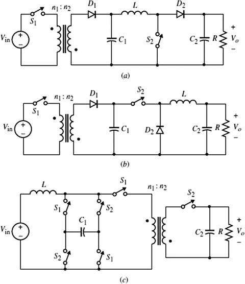
Fig. P5.26
-
(a)
\( \frac{V_{\mathrm{o}}}{V_{\mathrm{in}}}=\frac{D}{{\left(1-D\right)}^2}\frac{n_2}{n_1} \)
-
(b)
\( \frac{V_{\mathrm{o}}}{V_{\mathrm{in}}}=\frac{D^2}{\left(1-D\right)\ }\frac{n_2}{n_1} \)
-
(c)
\( \frac{V_{\mathrm{o}}}{V_{\mathrm{in}}}=\frac{-D}{\left(1-D\right)\left(1-2D\right)}\frac{n_2}{n_1} \)
-
(a)
-
5.27
The converter shown in Fig. P5.27a is another version of the forward converter. Assume ideal diodes and L m is the transformer magnetizing inductance. The switching waveforms for S 1, S 2, S 3, and S 4 are shown in Fig. P5.27. Assume RC ≫ T.
-
(a)
Sketch the current and voltage waveforms labeled on the figure.
-
(b)
Derive the voltage gain expression V o/V in.
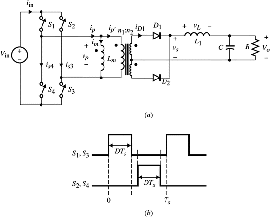
Fig. P5.27
-
(a)
-
5.28
Draw the waveforms for the branch currents and voltages for the push-pull converter by including a finite magnetic inductance as shown in Fig. P5.28.
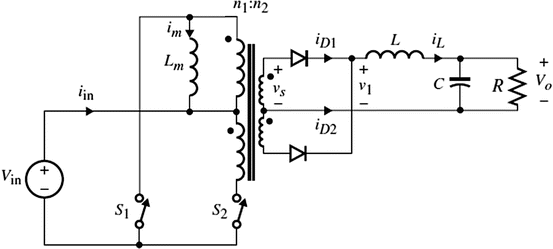
Fig. P5.28
-
5.29
(a) Show that if the single-ended flyback converter of Fig. 5.23b is operating in dcm (magnetizing current is discontinuous), then the voltage conversion ratio is given by:
$$ \frac{V_{\mathrm{o}}}{V_{\mathrm{in}}}=\frac{n_2}{n_1}D\sqrt{\frac{1}{2\tau }} $$where
$$ \tau =L/ RT $$ -
5.30
Consider the circuit given in Fig. P5.30 with the switching sequence given in Fig. P5.30:
-
(a)
Sketch the waveforms for i L, v s, \( {i}_{{\mathrm{D}}_1}, \) and \( {i}_{{\mathrm{D}}_4} \).
-
(b)
Derive the expression for V o/V in.
-
(c)
What is the expression for the critical value of L to maintain ccm of operation?
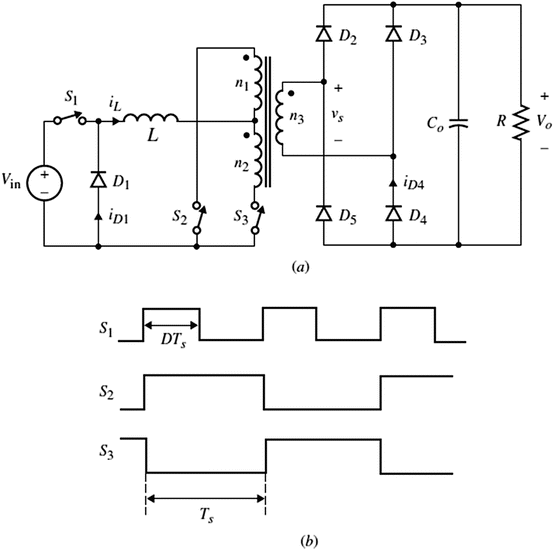
Fig. P5.30
-
(a)
-
5.31
There are several core reset schemes available in today’s dc-dc converters. Figure P5.31 shows one possible core resetting circuit used in high-power applications. The winding n r is the reset winding. (a) Discuss the operation of each circuit and compare them to each other and (b) draw the waveforms for i in, v sw, i o, v o, and \( {i}_{{\mathrm{D}}_1} \).
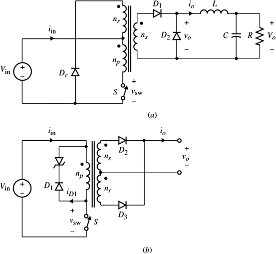
Fig. P5.31
-
5.32
Derive the voltage gain equation for the isolated double-switch, single-ended dc-dc converter in Fig. P5.32. S 1 and S 2 are switched simultaneously.
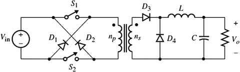
Fig. P5.32
-
5.33
Consider the current-fed push-pull converter given in Fig. P5.33. Derive the current gain expression I o/I in.
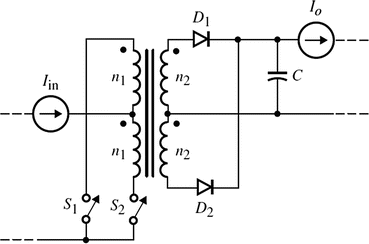
Fig. P5.33
-
5.34
The converter shown in Fig. P5.34 is an isolated version of the converter given in Chap. 4. Assume the magnetizing inductor is finite, L m. Drive the expression for V o/V in.
Fig. P5.34
-
5.35
Figure P5.35 shows the isolated version of the SEPIC converter, where a transformer is inserted in place of L 2. Assume the transformer has a magnetizing inductance, L m, and a turns ratio of n 1 : n 2.
-
(a)
Sketch the waveforms for i in, v sw, i o, v o, and \( {i}_{{\mathrm{D}}_1} \) and v sw.
-
(b)
Show that the voltage gain is given by:
$$ \frac{V_{\mathrm{o}}}{V_{\mathrm{in}}}=\frac{n_2}{n_1}\frac{D}{\left(1-D\right)} $$where D is duty cycle of the switch.
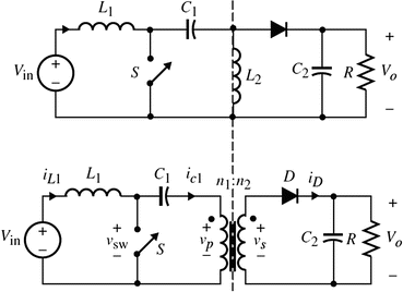
Fig. P5.35
-
(a)
-
5.36
The converter in Fig. P5.36a, b is known as the isolated Watkins-Johnson converter. Assume S 1 and S 2 are switched on and off as shown in Fig. P5.36c. Assume finite magnetizing inductance. Derive the expressions for V o/V in for each converter.
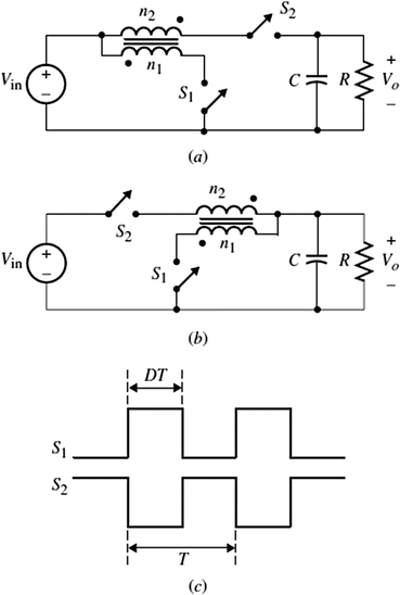
Fig. P5.36
-
5.37
Draw the waveforms for the voltage and current variables in the push-pull converter shown in Fig. P5.37. Unlike Fig. 5.16a, this converter assume finite magnetizing inductance.
Fig. P5.37
-
D5.38
Consider a flyback converter that draws its input current from a dc voltage source that varies between 185 V and 275 V and produces an output voltage of +12 V at an average load current of 10 A.
-
(a)
Determine the value of the transformer ratio and magnetizing inductance L m.
-
(b)
Determine the range of the duty cycle needed to maintain a constant output voltage. Assume f = 85 KHz and a maximum duty cycle of 0.6.
-
(a)
-
D5.39
Repeat the design in Problem P5.38 by assuming the power switch and diode have 3 V and 0.7 V voltage drops when conducting, respectively.
-
5.40
Determine the efficiency of the flyback converter of Fig. 5.28 of Example 5.6 by assuming its output diode has a voltage drop of 0.75 V, and the on resistance of the switch is 48 mΩ.
-
5.41
The Fig. P5.41a shows a forward convertor with resent winding and magnetizing inductor whose current waveforms are shown in Fig. P5.41b. Assume the convertor is operating in ccm with its output current and assume constant with ripple free. Based on the values shown, determine the convertor parameters and the primary-side magnetizing inductance.
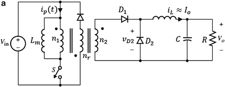
Fig. P5.41a
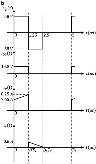
Fig. P5.41b


Rights and permissions
Copyright information
© 2018 Springer International Publishing AG
About this chapter

Cite this chapter
Batarseh, I., Harb, A. (2018). Isolated Switch-Mode DC-DC Converters. In: Power Electronics. Springer, Cham. https://doi.org/10.1007/978-3-319-68366-9_5
Download citation
DOI: https://doi.org/10.1007/978-3-319-68366-9_5
Published:
Publisher Name: Springer, Cham
Print ISBN: 978-3-319-68365-2
Online ISBN: 978-3-319-68366-9
eBook Packages: EngineeringEngineering (R0)