
Abstract
Nanoparticles (NPs) embedded in a conductive or insulating matrix play a key role in memristors and in flash memory devices. However, the role of proximity to the interface of isolated NPs has never been directly observed nor fully understood. Here we show that a reversible local switching in tunnel conductivity can be achieved by applying an appropriate voltage pulse using the tip of a scanning tunnelling microscope on NPs embedded in a TiO2 matrix. The resistive switching occurs in the TiO2 matrix in correlation to the NPs that are in proximity of the surface and it is spatially confined to the single NP size. The tunnel conductivity is increased by more than one order of magnitude. The results are rationalized by a model that include the charge of NPs that work as a nano floating gate inducing local band bending that facilitates charge tunnelling and by the formation and redistribution of oxygen vacancies that concentrate in proximity of the charged NPs. Our study demonstrates the switching in tunnel conductivity in single NP and provides useful information for the understanding mechanism or resistive switching.
Introduction
In the last decade existing CMOS technology has approached its physical limits1 resulting in a great deal of research toward novel devices and concepts. Non-volatile flash memories are one of the pivotal needs for knowledge–based development and a prime challenge for science and technology. Technology demands nanometric size (viz. high density), high speed, low power consumption, high retention time, chemical and thermal stability in memory elements whose nanofabrication technology must also be compatible with the present processes2.
Flash memory devices based on floating gate memories3 and memristors4,5 are recognised as the most likely candidates for the post-CMOS technology in nanoscale memory-bit cells and computation devices6. Both systems are quickly approaching the stage of industrial application; however, some important problems remain unsolved such as the limits of spatial resolution, where the switching occurs and the implication of the single NP at the interfaces.
Flash memory devices are based on single transistors with a floating gate. This consists of a conductive structure embedded in an insulating matrix that acts as a charge storage layer (floating gate electrode). The charge of the floating gate shifts the threshold voltage of the transistor, which can be set in a programmed state or in an erased state depending on the charging of the floating gate. The use of nanoparticles7 (NPs) or nanocrystals8 as novel architectures, named nano-floating gate memories9, are of enormous interest due to advantages in tunability of charge trapping sites, which can be controlled by the size and nature of the NPs. Furthermore, the ability to process them at room temperature using simple wet processes, their compatibility with flexible substrates and eventually the ease of integration with the current technology make them ideal candidates for new flash memory devices compatible with plastic electronics7.
Embedded NPs also have been proven to be very important in reversible resistive switching, whose corresponding devices, called memristors4,5, have received an enormous amount of interest in recent years, because of their versatility and simple architecture. In the basic configuration a memristor consists of an insulating/semiconducting thin film sandwiched between two electrodes, forming a Metal-Insulator-Metal (MIM) device. The resistive switching occurs after the application of a high electric field/high current pulse10. It has been proven that NPs greatly improve key parameters of memristors such as stability, on/off ratio, switching speed and in reduction of the current level11,12.
In this context, the investigation of the NPs in close proximity to the surface using scanning probe microscopy offers a unique opportunity to gain new information in the system, including, the possibility to reach the limit of spatial resolution and the possibility to investigate the sample interface after switching. Resistive switching by scanning probe microscopy has been proven at the sub-micrometric13,14,15,16,17 and nanometric scale18,19,20 in several systems but the role of single NP at interfaces has never been directly observed.
Here we show that a local reversible switching in tunnel conductivity can be performed at the level of a single NP by applying a voltage pulse using a scanning tunnelling microscopy (STM) tip on single NPs embedded in a TiO2 matrix. The switching in tunnel conductivity occurs in the TiO2 around the NP in proximity of the surface due to NP charge trapping and is spatially confined by the NP size. We performed our experiments at room temperature using prototypical materials which are commercially available and whose processing is well established. In particular we used TiO2 because it can be a good matrix in named nano-floating gate memories due to its high band-gap (~3.2 eV) and it is largely studied in memristors. Furthermore, the protocol for thin film preparation is very simple and largely reported in literature21. Cobalt NPs are commercially available by the major chemical suppliers or can be easily synthetized22. They consist of a Co spheres with a diameter range between 50 and 100 nm, covered by a thin layer of cobalt oxide and the surfactant, which allows for solubilisation in water. We used NPs with a diameter >50 nm in order to demonstrate that although the STM junction occurs in a few Angstroms, the resistive switching involves and is limited to the whole NP region.
Samples were characterized by scanning tunnelling microscopy (STM), scanning tunnelling spectroscopy (STS), atomic force microscopy (AFM) and by scanning kelvin probe microscopy (SKPM)23.
Results
Thin films 120 ± 15 nm thick of Co NPs embedded in TiO2 were obtained by spin coating a water solution of Bis(ammonium lactate)titanium dihydroxide and of cobalt NPs on a Au substrate, the film was then calcined at high temperature (see detail in methods). As a blank, a thin film of pure TiO2 was prepared following the same procedure.
Besides the occasional formation of large aggregates of NPs, AFM confirms the presence of Co NPs at the solid/air (vacuum) interface. The TiO2 matrix appears to be formed by a homogeneous distribution of clusters whose mean diameter is <15 nm with an r.m.s. roughness of about 1 nm. NPs appear as randomly distributed larger clusters whose size range from 50 to 100 nm (Fig. 1a) with a density at the surface ranging from <1 to 10 NPs μm2. NPs can be fully embedded in the matrix appearing as larger clusters, or partially embedded, appearing as outgrowths a few nm thick. The evidence that the outgrowths and larger clusters are not formed by different aggregations of TiO2 is established by SKPM that shows an evident contrast between aggregations of TiO2 and NPs (Fig. 1b). NPs exhibit a typical metallic behaviour24,25. Outgrowths were rarely observed in blank samples nor do they show contrast at SKPM. Figure 1 shows a typical morphology of NPs embedded in the matrix and the corresponding surface potential maps.

(a) AFM morphology recorded in intermittent contact mode of cobalt nanoparticles embedded in TiO2 matrix (Z scale 0–15 nm) and (b) the corresponding scanning kelvin probe microscopy.
The electronic structure of the samples were characterized by STM/STS, which features sensitivity to the local electronic structure. In particular we used current imaging tunneling spectroscopy (CITS), in which the tip is scanned in the constant current mode to maintain a constant distance to the sample. At each point the feedback loop is disabled and a defined number of I/V curve are recorded.
Since the NPs can locally affect the film morphology, NPs used for our experiment were selected making a large scale image at the maximum scan range of the piezo system of STM (3 × 3 μm2 in our set-up) selecting only the well-embedded NPs (e.g. NPs that emerge from the surface <10 nm).
Although, occasionally, some outgrowths exhibit a higher Tunnel Conductivity (TC) than the matrix, most likely due to the local formation of defects26 or to two-dimensional phases with reduced bandgap27; the CITS map appear generally homogeneous with a TC of about 10 pA/V recorded at −1 V bias (Fig. 2a), which is almost equal to the TC of the blank samples.

STM and tunnel conductivity map of a Co NP embedded in TiO2 matrix.
Topographic images were recorded at −1.5 V and levelled by 2nd order line. (a) Topography before conditioning, the regular distribution of small spikes is generated by the acquisition of the corresponding CITS map (Z scale 0–5 nm). (b) Corresponding tunnel conductivity (TC) map of “a” recorded at −1 V. The spectroscopic points are recorded with a resolution 5 times less than the topography. Z scale 0–−50 pA/V, Bright zones correspond to lower TC. (c) Topography after conditioning applying a single pulse of +5 V for 50 ms in the position indicated by the red cross in “a” (Z scale 0–5 nm). (d) TC map after the conditioning (switching) recorded at −1 V. While the topography remains unaltered, the NP at the centre of the image switches from a low conductive state to a high conductive state; the process is reversible.
The TC can be locally switched in correlation to the particular NPs by applying an appropriate voltage pulse (tip conditioning). When a positive pulse, higher than +5 V and longer than 10 ms, was applied in correspondence to the NP (Note: these parameters depend on the current of the set-point used before the pulse), we observed a dramatic change of TC that switches in a conductive state more than one order of magnitude higher than the matrix (HCS). The effect is not observed applying pulses in between the NPs and in blank samples. When applying pulses shorter than 100 ms the morphology remains unaltered, on the other hand, upon applying a longer and/or higher bias we observed a progressive damaging of the surface associated to the increase of TC. Figure 2 shows the effect of conditioning on isolated NPs after applying a pulse of +5 V for 50 ms.
It must be noted that while the STM junction occurs in a few Angstroms (≪ than 1 pixel in the TC map), the resistive switching involves and is limited to the whole NP region. The change of TC is reversible upon applying a negative pulse bias. However, while switching a NP to HCS can be easily performed by a single pulse, the inverse process is more difficult and several scans or pulses at large negative bias are necessary to reset the system which shows a progressive decreasing of TC instead of a single switching event. We were not able to switch the system in high HCS by applying negative bias. Upon increasing the time of conditioning up to 300 ms the surface of blank TiO2 can also be modified. In this last case both positive and negative bias have the same effect producing a moderate increase of the TC. In this last case the conditioning dramatically damages the surface in an area of a few hundred nanometers and it is not reversible. We propose that in this case the electric field and current density are high enough to cause a thermal recrystallization forming the so called filaments. This phenomenon is well known and it is believed to be responsible for the so called “forming” step in conventional memristor based on TiO2 in MIM structures5,28.
A detailed study of the I-V curves (Fig. 3), helps us to identify the nature the resistive switching on single NP. The I-V curves recorded in a clean sample, before the resistive switching, show the normal behaviour of freshly prepared TiO226,29, both in the matrix and in relation to the NPs (Blue curve). The typical trend of a n-type semiconductor with an asymmetric band-gap of ~3.2 eV is expressed by the zero conductance region around 0 V bias (Curve bleu in fig. 3). This behaviour indicates that a thin layer of TiO2 also covers the partially embedded NPs. Very rarly, exposed NPs exhibiting metallic behaviour in I-V curves were observed by STM, we excluded these zones from our experiments. Figure 3 shows the I-V curves recorded corresponding to the NP during the application of +5 V pulse bias for 50 ms and the corresponding dI/dV curve.

Scanning tunnelling spectroscopy.
(a) I-V curves extracted from current imaging tunnelling spectroscopy (CITS) map, before (blue curve) and after (red curve) the conditioning of the nanoparticle. The process is reversible. The curve after conditioning was limited in the range −2.5 V–+1 V in order to prevent out of range of the STM current. (b) Corresponding dI/dV curve local density of the surface states.
Since the pulse bias does not alter the matrix, the I-V curves observed before the resistive switching are the typical curves of TiO2. After resistive switching, the curves recorded in correspondence to the NPs narrows the zero conduction region from ~3.2 to ~2 eV (Fig. 3b). Noticeably this reduction occurs only in the negative branch of the curve (i.e. when the electrons move from the tip to the surface) while the positive branch remains almost unaltered. This indicates that some empty surface states are formed in the zone corresponding the NPs, with energy ~1 eV below the conduction band of TiO2. The I-V curve comes back in the original state as the transition is reset by applying negative pulses.
Discussion
About the resistive switching that occurs only in correspondence to the NPs we speculate on the contribution of two effects:
-
i
The charge injection inside a NP8,30, which occurs at a high bias by direct tunnelling in the NP. This is confirmed by the TC changes upon conditioning over the entire NP region, not only under the tip during the switching pulse. The switching in TC is not observed in blank samples, unless the dramatic damage of the surface (TiO2 recrystallization).
As observed in previous literature31, the positive pulse injects holes into the NP, which become positively charged. The charged NPs in proximity of the surface, work as a floating gate, inducing a band bending towards a lower energy state due to the electrons in the TiO2 being attracted by the charged NPs. These states are present in the thin layer in between the STM tip and the surface become accessible as empty states for tunnelling from the STM tip (Fig. 4b) at energy below the conduction band of TiO2.
Figure 4 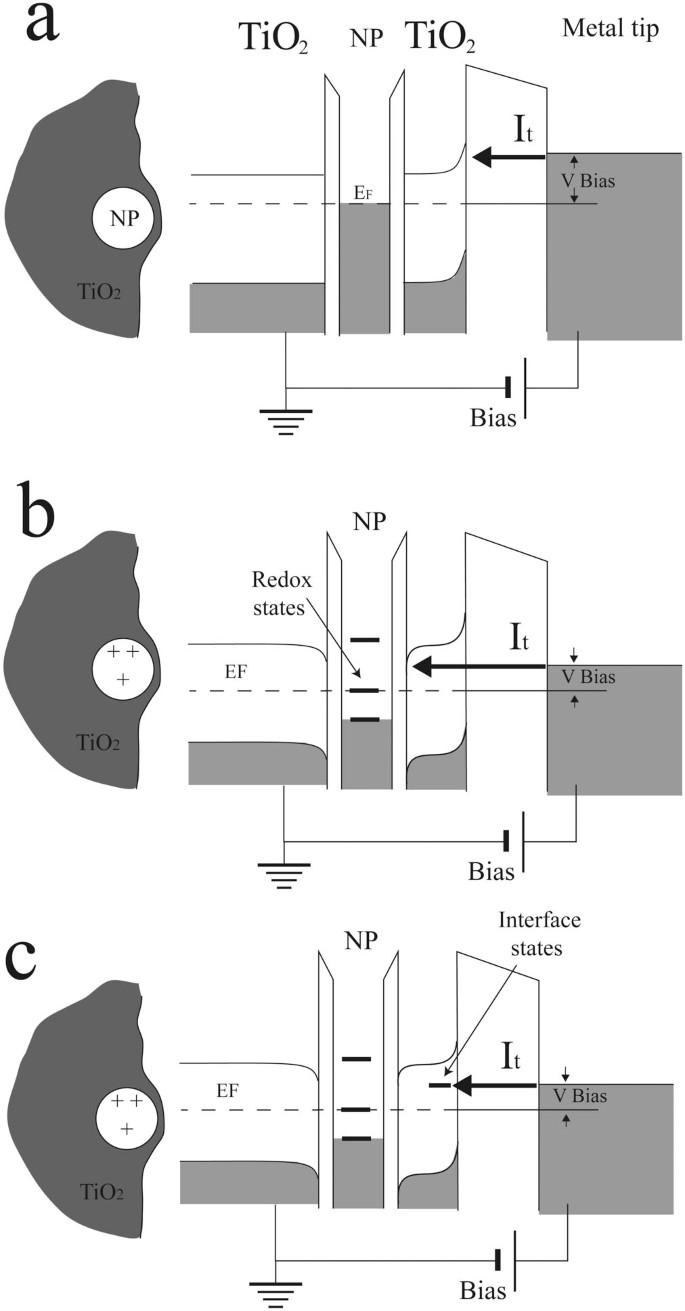
Scheme of switching of tunnel conductivity.
(a) Normal sample/insulating/metal STM junction (b) Effect of charge trapping of the NP that induces a band-bending of TiO2 which became directly accessible for tunnelling of electrons from the tip. (c) Effect of oxygen vacancies movements toward the conditioned zone in between the nano particle and the STM tip.
The injection of electrons in a positively charged NP discharges the NP, thereby resetting the system.
-
ii
A further contribution to resistive switching can be provided by the formation and redistribution of oxygen vacancies that are intrinsically present TiO2 matrix. By applying pulse bias, the oxygen vacancies form and move toward tip/TiO2/NP interface forming undefined TiOx chemical species, which in turn may create interface state and/or reduce barrier height. Such a reduced barrier effect is well known in Pt/TiO2/Pt memristor system32 (Fig. 4c). In addition, NPs may enhance the effect as recently observed for ruthenium nano-dots embedded in TiO212. Figure 4 shows a scheme of the proposed switching mechanisms in TC.

For both models the possible origin of the asymmetry in the switching behaviour (i.e. the fact that the switching only occurs by injecting holes but does not work when injecting electrons) can be attributed to the redox states in the NPs related to the oxidation of some Co atoms, which form Co ions positively charged, as previously observed in Co NPs deposited on graphite33. The injection of electrons should include an improbable chemical reduction of Co atoms.
In summary, we used STM to study the effect of NPs embedded in a TiO2 matrix on the switching of tunnel conductivity. We have shown how resistive switching occurs in the surface state of the thin layer of TiO2, in proximity of the NPs and is spatially confined in the region between the NPs and the surface. The formation of empty surface states locally enhances the tunnel conductivity reducing the apparent band-gap of the TiO2. Using STM we measured the NPs on the surface, however we expect that the similar mechanism of TC switching occurs also inside the matrix, in this case the process involve two NPs instead a NPs and the STM tip. Here we proposed two possible contributions to TC switching, however we do not exclude that other effects could contribute to the observed switching. In forthcoming work, details of TC switching mechanism will be further investigated. In addition, the size of NPs can be significantly reduced to a few nanometres. This ongoing work will lead a better understanding of the role of NPs in resistive switching and leads to new possibilities for NP integration in nano floating gate memories and other electronic devices34,35.
Methods
Thin films
Pieces 11 × 11 mm2 borosilicate glass covered by Cr (2.5 nm) and Au (250 nm) were used as substrates. Thin films were fabricated by spin coating (1500 r.p.m., 60 s) of 150 μl of a solution of Bis(ammonium lactate)titanium dihydroxide (TALH) 5% (Aldrich) and 1.25% of Cobalt nanoparticles (Aldrich) in ultrapure water. All the reagents were used as received. In order to remove possible aggregates all solution were filtered through a 0.22 μm RC membrane filter. Blank samples were prepared using pure TALH solution.
In order to transform the precursor into crystalline anatase TiO2 the samples were calcined at 450°C in air using a thermal ramp of 2°C/min followed by a 2 h stationary step at 450°C.
The film appears to be formed by a homogeneous distribution of clusters whose mean diameter is <15 nm with an r.m.s. roughness ~1 nm. NPs, whose size range from 50 to 100 nm where as randomly distributed with a density at the surface ranging from <1 to 10 NPs μm2. The film thickness (120 ± 15 nm) was measured by AFM scratching the surface by a doctor blade.
Scanning tunnelling microscopy
The STM-STS experiments were carried out at room temperature under Ultra High Vacuum (UHV) conditions using a commercial tip-biased Omicron STM. All measures were performed using manually cut Pt/Ir tips or by the set-up described in ref. 36,37. Images were acquired at 512 × 512 points in topographic mode. The topographic maps were unfiltered but leveled by 2nd order line.
NPs were recognized from the topographic image according to AFM image. They are recognized as outgrowth or larger clusters.
Scanning tunnelling spectroscopy
The STS maps were performed using current imaging tunnelling spectroscopy (CITS) technique, in which the tip is scanned in the constant current mode to maintain a constant distance to the sample. Every 5 points of topography the feedback loop is disabled and 100 I/V curves are recorded. Each pixel of the CITS map is the mean curve. I(V) local spectra were acquired by ramping the bias voltage from −2 to +1.2 V in order to prevent the current saturations in the high conductive zones. Meanly we acquired from 3000 to 15.000 curves/image.
Conditionings
Tip-conditionings at positive/negative biases were carried out maintain the STM in the topographic mode. The feedback loop is disconnected during the conditioning.
The conditioning were tested in the range of 4 ÷ 7 Volts, applied for 10 to 600 ms.
Occasionally purely metallic behavior was observed in correspondence of the NP after tip conditioning at bias higher than 5 V and longer than 300 ms.
References
Vogel, E. M. Technology and metrology of new electronic materials and devices. Nat. Nanotechnol. 2, 25–32 (2007).
Cavallini, M. et al. Regenerable Resistive Switching in Silicon Oxide Based Nanojunctions. Adv. Mater. 24, 1197–1201 (2012).
Pavan, P., Bez, R., Olivo, P. & Zanoni, E. Flash memory cells - An overview. Proc. IEEE 85, 1248–1271 (1997).
Chua, L. Resistance switching memories are memristors. Appl. Phys. A: Mater. Sci. Process. 102, 765–783 (2011).
Strukov, D. B., Snider, G. S., Stewart, D. R. & Williams, R. S. The missing memristor found. Nature 453, 80–83 (2008).
Borghetti, J. et al. ‘Memristive’ switches enable ‘stateful’ logic operations via material implication. Nature 464, 873–876 (2010).
Kang, M., Baeg, K.-J., Khim, D., Noh, Y.-Y. & Kim, D.-Y. Printed, Flexible, Organic Nano-Floating-Gate Memory: Effects of Metal Nanoparticles and Blocking Dielectrics on Memory Characteristics. Adv. Funct. Mater. 23, 3503–3512 (2013).
Yang, R. et al. Isolated nanographene crystals for nano-floating gate in charge trapping memory. Sci. Rep. 3, 2126; 10.1038/srep02126 (2013).
Hanafi, H. I., Tiwari, S. & Khan, I. Fast and long retention-time nano-crystal memory. IEEE Trans. Electron Devices 43, 1553–1558 (1996).
Yang, Y. C. et al. Observation of conducting filament growth in nanoscale resistive memories. Nat. Comm. 3, 732 (2012).
Choi, B. J. et al. Electrical Performance and Scalability of Pt Dispersed SiO2 Nanometallic Resistance Switch. Nano Lett. 13, 3213–3217 (2013).
Yoon, J. H. et al. Highly Improved Uniformity in the Resistive Switching Parameters of TiO2 Thin Films by Inserting Ru Nanodots. Adv. Mater. 25, 1987–1992 (2013).
Gruverman, A. et al. Tunneling Electroresistance Effect in Ferroelectric Tunnel Junctions at the Nanoscale. Nano Lett. 9, 3539–3543 (2009).
Yin, K. B. et al. Resistance switching in polycrystalline BiFeO3 thin films. Appl. Phys. Lett. 97, 042101 (2010).
Szot, K., Dittmann, R., Speier, W. & Waser, R. Nanoscale resistive switching in SrTiO3 thin films. Phys. Status Solidi-R R L 1, R86–R88 (2007).
Hong, S. S., Cha, J. J. & Cui, Y. One Nanometer Resolution Electrical Probe via Atomic Metal Filament Formation. Nano Lett. 11, 231–235 (2011).
Pantel, D., Goetze, S., Hesse, D. & Alexe, M. Room-Temperature Ferroelectric Resistive Switching in Ultrathin Pb(Zr0.2Ti0.8)O-3 Films. ACS Nano 5, 6032–6038 (2011).
Chen, Y. L. et al. Scanning tunneling microscopy/spectroscopy studies of resistive switching in Nb-doped SrTiO3 . J. Appl. Phys. 112, 023703 (2012).
Dubost, V. et al. Resistive Switching at the Nanoscale in the Mott Insulator Compound GaTa4Se8. Nano Lett. 13, 3648–3653 (2013).
Hota, M. K., Bera, M. K. & Maiti, C. K. Direct Nanoscale Observation of Resistance Switching with Au Nano-Dots Embedded Nb2O5 by Scanning Tunneling Microscopy. Nanosci. Nanotechnol. Lett. 4, 394–399 (2012).
Dionigi, C. et al. 3D Hierarchical Porous TiO2 Films from Colloidal Composite Fluidic Deposition. Chem. Mat. 20, 7130–7135 (2008).
Lu, A. H., Salabas, E. L. & Schuth, F. Magnetic nanoparticles: Synthesis, protection, functionalization and application. Angew. Chem., Int. Ed. 46, 1222–1244 (2007).
Liscio, A., Palermo, V. & Samori, P. Nanoscale Quantitative Measurement of the Potential of Charged Nanostructures by Electrostatic and Kelvin Probe Force Microscopy: Unraveling Electronic Processes in Complex Materials. Acc. Chem. Res. 43, 541–550 (2010).
Nonnenmacher, M., O'Boyle, M. P. & Wickramasinghe, H. K. Kelvin probe force microscopy. Appl. Phys. Lett. 58, 2921–2923 (1991).
Liscio, A., Palermo, V., Mullen, K. & Samori, P. Tip-Sample Interactions in Kelvin Probe Force Microscopy: Quantitative Measurement of the Local Surface Potential. J. Phys. Chem. C 112, 17368–17377 (2008).
Lin, Y., Lin, R., Wang, W. & Xiao, X. Characterization of TiO2 nanocrystalline thin film by scanning tunneling microscopy and scanning tunneling spectroscopy. Appl. Surf. Sci. 143, 169–173 (1999).
Tao, J. G., Luttrell, T. & Batzill, M. A two-dimensional phase of TiO2 with a reduced bandgap. Nature Chem. 3, 296–300 (2011).
Kwon, D. H. et al. Atomic structure of conducting nanofilaments in TiO2 resistive switching memory. Nat. Nanotechnol. 5, 148–153 (2010).
Berkó, A. & Solymosi, F. Study of Clean TiO2(110) Surface by Scanning Tunneling Microscopy and Spectroscopy. Langmuir 12, 1257–1261 (1996).
Lee, C., Kim, I., Shin, H., Kim, S. & Cho, J. Nonvolatile memory properties of Pt nanoparticle-embedded TiO2 nanocomposite multilayers via electrostatic layer-by-layer assembly. Nanotechnology 21, 185704 (2010).
Yang, J. et al. Electrostatic force microscopy measurements of charge trapping behavior of Au nanoparticles embedded in metal-insulator-semiconductor structure. Ultramicroscopy 108, 1215–1219 (2008).
Yang, J. J. et al. Memristive switching mechanism for metal/oxide/metal nanodevices. Nat. Nanotechnol. 3, 429–433 (2008).
Fetting, J. et al. I-V characteristics of single and clustered ligand stabilized cobalt nanoparticles on highly oriented pyrolytic graphite obtained with conducting atomic force microscopy under ambient conditions. J. Appl. Phys. 112, 104327 (2012).
Cavallini, M. et al. Additive nanoscale embedding of functional nanoparticles on silicon surface. Nanoscale 2, 2069–2072 (2010).
Simeone, F. C., Albonetti, C. & Cavallini, M. Progress in Micro- and Nanopatterning via Electrochemical Lithography. J. Phys. Chem. C 113, 18987–18994 (2009).
Cavallini, M. & Biscarini, F. Electrochemically etched nickel tips for spin polarized scanning tunneling microscopy. Rev. Sci. Instrum. 71, 4457–4460 (2000).
Cavallini, M., Aloisi, G., Bracali, M. & Guidelli, R. An in situ STM investigation of uracil on Ag(111). J. Electroanal. Chem. 444, 75–81 (1998).
Acknowledgements
We thank Zhara Hemmatian Denis Gentili and Vittorio Morandi for sample preparation and SEM measurements and Tobias Cramer for the useful discussion and the help to model the process and Laurel L. McClure for editing the manuscript. A.G. was supported by EU-FP7 project NMP3-LA-2010-246102 (IFOX), the work was partially supported by “Progetto bandiera NANOMAX-N-CHEM”.
Author information
Authors and Affiliations
Contributions
A.G. was responsible for all the experiments described in this article; M.P. was partially responsible for preparation of the paper and modeling; M.C. was responsible for designing and providing guidance for the experiments and for editing and proofreading the paper. All the authors contributed to write the manuscript.
Ethics declarations
Competing interests
The authors declare no competing financial interests.
Rights and permissions
This work is licensed under a Creative Commons Attribution-NonCommercial-NoDerivs 3.0 Unported License. To view a copy of this license, visit http://creativecommons.org/licenses/by-nc-nd/3.0/
About this article
Cite this article
Gambardella, A., Prezioso, M. & Cavallini, M. Tunnel conductivity switching in a single nanoparticle-based nano floating gate memory. Sci Rep 4, 4196 (2014). https://doi.org/10.1038/srep04196
Received:
Accepted:
Published:
DOI: https://doi.org/10.1038/srep04196
This article is cited by
-
Probing electrochemistry at the nanoscale: in situ TEM and STM characterizations of conducting filaments in memristive devices
Journal of Electroceramics (2017)
-
Single-Readout High-Density Memristor Crossbar
Scientific Reports (2016)
Comments
By submitting a comment you agree to abide by our Terms and Community Guidelines. If you find something abusive or that does not comply with our terms or guidelines please flag it as inappropriate.
