

Abstract
Defects are usually seen as imperfections in materials that could significantly degrade their performance. However, at the nanoscale, defects could be extremely useful since they could be exploited to generate novel, innovative and useful materials and devices. Graphene and graphene nanoribbons are no exception. This review therefore tries to categorize defects, emphasize their importance, introduce the common routes to study and identify them and to propose new ways to construct novel devices based on 'defective' graphene-like materials. In particular, we will discuss defects in graphene-like systems including (a) structural (sp2-like) defects, (b) topological (sp2-like) defects, (c) doping or functionalization (sp2- and sp3-like) defects and (d) vacancies/edge type defects (non-sp2-like). It will be demonstrated that defects play a key role in graphene physicochemical properties and could even be critical to generate biocompatible materials. There are numerous challenges in this emerging field, and we intend to provide a stimulating account which could trigger new science and technological developments based on defective graphene-like materials that could be introduced into other atomic layered materials, such as BN, MoS2 and WS2, not discussed in this review.
Export citation and abstract BibTeX RIS
This article was invited by M-Y Chou
1. Introduction
John Desmond Bernal in his seminal paper on the structure of graphite in 1924 recognized the previous difficulties of the proposed structures by Hull [1], and Debye and Scherrer in 1917 [2] due to their lack of highly crystalline samples. Bernal solved the crystal structure of graphite using x-ray diffraction with the crystal rotation technique on a very good quality natural crystal of ceylon graphite (see figure 1(a)) [3]. Lipson and Stokes reported in 1942 that the graphitic layers could also have a different order, not the ab, ab, ... stacking reported by Bernal, but abc, abc, ... rhombohedral stacking [4]. Gibson in 1946 reported that the structure with abc, abc, ... stacking was actually the structure reported by Debye and Scherrer in 1917 [5]. A few years later, Rosalind Franklin in 1951 described non-graphitic turbostratic carbons where stacking symmetry was not preserved and exhibited an interlayer spacing of 3.44 Å, slightly larger than the 3.35 Å spacing of graphite [6].
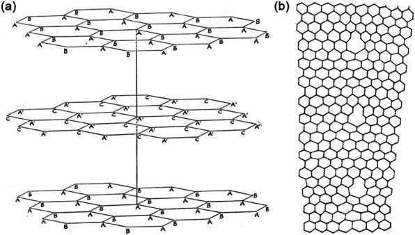
Figure 1. (a) Original drawing by Bernal describing the structure of graphite. Reprinted with permission from [3]. Copyright 1924 by The Royal Society. (b) Roscoe and Thomas model for a grain boundary. Note that bonds are not drawn in the defective regions. Five–seven defects can be drawn avoiding dangling bonds. Reprinted with permission from [7]. Copyright 1966 by Elsevier Ltd.
Download figure:
Standard imageFor these intervening 30 years, the main topic of graphite-related study involved the disorder or relative order of the constituent graphene layers, and did not concentrate on the study of individual layers. In the 1960s researchers started to focus on defects within individual layers, such as vacancies, interstitials and grain boundaries. Peter Thrower studied the role of vacancies and interstitials in the self-diffusion in graphite, and also the formation of interstitials and vacancy loops in graphite under high irradiation [8–10]. Amelinckx and colleagues also studied dislocations in graphite by the most advanced transmission electron microscopy (TEM) techniques then available [11, 12]. In 1966 Roscoe and Thomas [7] proposed a small angle grain boundary exhibiting heptagon–pentagon pairs but, for some unknown reason, they did not draw all the bonds in their published figures (see figure 1(b)).
Study of the intercalation of ions and molecules into graphite started in the 1960s and became better known in the 1970s. The intercalation process inserts guest species between graphite layer by a controlled method and is used to generate large electron or hole carrier concentrations in the graphene layers [13]. The staging phenomenon whereby a single intercalant layer can be inserted periodically between graphene layers (up to perhaps seven layers) provides an example of the use of controlled defects to change material behaviors by providing the host materials with unusual and well-controlled properties [13].
Systematic studies of defects started to be carried out in 1981 when Elman used ion implantation to create point defects in graphite [14]. In these studies the amount of lattice damage was controlled by the ion mass and its energy, with low mass ions such as 11B ions implanted at 20 keV and a fluence of 1012 ions cm−2, thereby providing low levels of damage [14]. Typical control parameters that were used include ion species of different masses ranging from boron to bismuth, ion energies from 20 to 200 keV and ion fluences from 1012 to 1015 ions cm−2. The experimental characterization techniques used at that time were x-ray diffraction, TEM for structural studies, Raman and infrared (IR) spectroscopy for studying structural damage effects on the phonon response, and transport measurements to assess the damage to the electronic properties. The findings of these defect studies are summarized in some detail in a book written on the subject of ion implantation in graphite [15]. Similar experimental approaches plus some new techniques, such as scanning tunneling probes, have recently been used more quantitatively to study controlled defects in graphene using similar ion implantation techniques with some further advances [16].
With the discovery of Buckminsterfullerene or carbon 60 (C60) in 1985, a new area in carbon science started, not only because C60 was a newly found carbon molecule but also because C60 could be seen as a finite high symmetry graphitic nanostructure containing 20 hexagonal rings and 12 pentagonal rings of carbon that were required to close the molecular structure [17]. The icosahedral C60 structure is highly stable against random defect formation, which can be documented by the 200 or so different IR-active modes and ∼200 Raman-active modes that can be reproducibly observed. These modes are associated with the high icosahedral symmetry of the C60 molecule [18]. Soon after the bulk synthesis of C60 [19, 20], intense theoretical and experimental work followed [18] and the quest for new sp2-like carbon cage molecules (known as fullerenes) began. In this context, the idea of elongating these carbon cages along one direction was introduced. As a result of this elongation, carbon nanotubes were predicted [21–23]. The synthesis and chirality identification of single-walled carbon nanotubes (SWCNTs) by electron diffraction was soon reported [24]. It is important to mention that SWCNTs and multi-walled carbon nanotubes (MWCNTs) were observed as early as the 1970s by Endo using high-resolution transmission electron microscopy (HRTEM) [25]. The reader is encouraged to read some nanotube reviews or related books that have been published elsewhere [18, 26]. From the above paragraphs, it is clear that intense research into the nanocarbon world started in the late 1980s and had continued with the discovery and isolation of other forms of carbon including graphene, graphene nanoribbons, platelets, doped CNTs, etc.
In 2004 a series of experiments showed that graphene, an individual sheet of graphite, could be isolated and these experiments showed unique and exciting physicochemical properties different from those observed in graphite, and a new field dedicated to atom-thick 2D carbon materials started [27–30]. The early entry of Boehm into the monolayer graphene field in 1961 was recognized, and it was Boehm who gave graphene its name [31–33]. In 2010, Chuvilin and colleagues showed the transformation of a graphene surface into a fullerene using a transmission electron microscope [34], thus showing that fullerenes are indeed a metastable state of graphene. In summary, one could transform graphene into fullerenes, graphene into nanotubes, fullerenes into nanotubes or nanotubes into graphene nanoribbons. These transformations are all possible and have been demonstrated from both a theoretical and experimental standpoint [34–37]. This makes carbon so diverse. It is fascinating to witness that a very old and common element, such as carbon, is capable of forming all of these novel morphologies with unusual properties. We foresee that other novel and exotic carbon nanostructures will be synthesized and predicted in the years to come, though it is difficult to predict the new forms of carbon that will someday appear, but hybrid materials incorporating graphene, nanotubes, nanoribbons, fullerenes and diamond could be a promising new research direction for future focus.
For graphene, defects occur within a single monolayer. For few-layer graphene, interlayer-type defects such as stacking faults also occur. Thus, the physicochemical properties of monolayer and few-layer graphene depend not only on the presence of defects but also on the defect type, the defect environment and the arrangement of ensembles of defects. In this account, several defects that appear in graphene are reviewed and studied, and several challenges associated with their atomic characterization and control are discussed. The study of defects in graphene is special because graphene is the most fundamental form of sp2 hybridized carbon, and what we learn from the study of each defect can then be used as a basis for understanding related defects occurring in sp2-like carbons more generally.
2. Graphene and graphene nanoribbons
In this section, we summarize the structure and properties of graphene and graphene nanoribbons in their pristine forms, prior to the introduction of defects.
2.1. Graphene
Graphene consists of a single and infinite layer of graphite in which each carbon atom possesses an sp2 hybridization. By hybridization we mean that each carbon atom is connected to three other carbon atoms via covalent bonds with lengths of 1.42 Å and with 120° angles between each bonded pair (see figure 2). In addition, graphene could be considered as a network consisting of two triangular sublattices in which the electronic states form two energy bands intersecting at the K and K' points in the Brillouin zone, and these high symmetry points K and K' are connected by inversion symmetry. Close to these crossing points, the electron energy E(k) depends linearly on the wave vector k obeying the relativistic Dirac equation; thus electrons and holes in monolayer graphene are called Dirac fermions and points K and K' in reciprocal space are called Dirac points [28]. Dirac fermions are responsible for many new phenomena in physics, which for the case of graphene cause the anomalous integer quantum Hall effect at room temperature [30, 38], insensitivity to external electrostatic potentials (Klein paradox), jittery motion of the wave function (zitterbewegung) under confining potentials, and huge mean free paths (carrier mobilities of more than 100 000 cm2 V−1 s−1) [29, 39]. Experiments by the Manchester group in 2004 with few-layer graphene opened up a new research era on 2D layered materials [27]. However, the amazing properties of graphene change by adding additional layers, thus losing the real 2D character and also the Dirac fermion behavior [40–42]. To date, intensive experimental and theoretical studies of bilayer and tri-layer graphene have also taken place, including studies of different interlayer stacking orders.
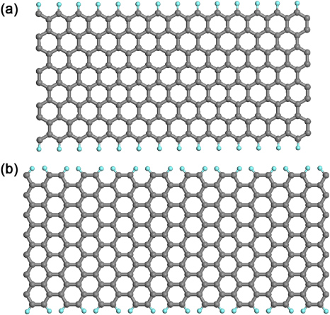
Figure 2. Molecular models of graphene nanoribbons with different edge morphologies: (a) an eight-zigzag graphene nanoribbon (8-ZGNR). (b) A 14-armchair graphene nanoribbon (14-AGNR). The edges of both nanoribbons are here saturated with hydrogen (cyan) atoms so that all the in-plane carbon bonds are satisfied.
Download figure:
Standard image2.2. Graphene nanoribbons: edge structure, width and electronic properties
Fujita and colleagues realized that, as in all realistic crystal structures, graphene should have edges, in this case one dimensional (1D) edges, which in the context of unzipped CNTs can be regarded as graphene ribbons, with armchair edges and zigzag edges as the two special high symmetry cases (see figure 2) [43, 44]. Therefore, in this context, armchair graphene nanoribbons (AGNRs) exhibit different widths depending on the number 'NA' of dimer lines across the ribbon width (NA-AGNRs), and likewise for zigzag graphene nanoribbons (ZGNRs) with a corresponding number 'NZ' for NZ-ZGNRs) (see figure 2).
Within a tight-binding approach, AGNRs could be metallic or semiconducting depending on their ribbon width, but all ZGNRs are metallic, with a high density of electronic states (DOS) at the edges. Therefore ZGNRs exhibit characteristic edge effects which are not present in AGNRs. These edge effects in ZGNRs are responsible for a flat band close to the Fermi level which implies a peak in the electronic density of states, thus making the ZGNR edges more reactive [43, 44]. These fundamentally different edge properties for ZGNRs and AGNRs provide a handle toward distinguishing armchair from zigzag edges at the nanoscale using local optical techniques which usually operate at the micrometer (10−6m) size level. When using first-principles calculations, all ZGNRs and AGNRs possess non-zero, direct band gaps. For ZGNRs the gaps are mini-gaps caused by spin ordering effects at the edges, and for AGNRs the band gaps arise from quantum confinement effects and can have larger magnitudes than for ZGNRs [45]. If spin polarization is considered in ZGNRs and quantum transport is studied, a band gap appears close to the Fermi level for the most stable antiferromagnetic configuration in which the total spin within the unit cell is zero: the spin is antiparallel across the zigzag edges (up at one side and down at the other side across the ribbon). However, a metastable ferromagnetic conducting configuration could also be calculated with an energy difference, from the antiferromagnetic case, of a few tens of meV [45, 46]. In the ferromagnetic case, the total spin within the unit cell is not zero and both zigzag edges across the ribbon in the unit cell exhibit parallel spin orientations.
For GNRs, the band gap decreases as the ribbon width increases, so if a semiconductor with a desirable band gap is needed, then the nanoribbon width should be reduced accordingly. This, of course, requires very precise control over the edges and widths of an AGNR, if applications are envisaged [45, 47, 48]. The bottom-up synthesis of graphene nanorribbons of different topologies and widths has been reported by Cai and colleagues [49]. In this work, using surface-assisted coupling of molecular precursors into linear polyphenylenes and a subsequent cyclodehydrogenation, 'chevron-like' GNRs are fabricated (see figure 3(a)). With this in mind, Costa-Girao et al have shown theoretically that the mixture of armchair and zigzag nanoribbons, called 'graphitic nanowiggles' (see figure 3(b)), exhibit different band gaps and magnetic behaviors, depending on the mixture of armchair and zigzag character within the same nanostructure [50].
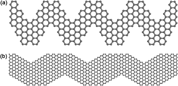
Figure 3. Molecular model of (a) a 'chevron-like' graphene nanoribbon and (b) a graphitic nanowiggle exhibiting a combination of armchair and zigzag edges.
Download figure:
Standard imageArmchair and zigzag edges in highly oriented pyrolytic graphite (HOPG) have been characterized using scanning tunneling microscopy (STM) and scanning tunneling spectroscopy (STS), finding electronic states close to the Fermi level for zigzag edges, and defective armchair edges, but not for homogeneous armchair edges [51–53]. Using a sub-nanometer-resolved STM-STS technique, Tao et al examined the dependence of electronic structure on the chirality of atomically well-defined GNR edges [54]. The GNRs they used were synthesized by unzipping CNTs [55]. Zigzag edges were observed by STM, and the finite width of the GNR leads to no actual band gap, which can be attributed to the reduced on-site Coulomb repulsion. Interestingly, the existence of spin-polarized magnetic edge states in chiral GNRs was also observed [54]. Along this line, some theoretical calculations on chiral graphene edges have also been carried out [56–59].
As in 3D crystals, graphene sheets and GNRs exhibit defects which result in significant changes in their physicochemical properties, and these should be studied in order to understand their properties with particular attention given to special kinds of defective 2D layered materials that could lead to novel applications. In this paper, we focus on the role of defects in these systems, how to control the defect behaviors and how perhaps to utilize some of these behaviors for practical applications.
2.3. Synthesis and characterization of graphene and graphene nanoribbons
The following subsections describe the various ways of producing graphene, few-layered graphene and graphitic nanoribbons. The methods range from the chemical vapor deposition (CVD) technique to the chemical longitudinal unzipping of CNTs. Novel routes are constantly being found and we expect that, with effort and proper know-how, it will be possible to achieve some control of the atomic edge morphology at the nanoscale. Until now, only a few methods have been able to report short segments of atomically controlled and/or smooth edges for GNRs [42].
2.3.1. CVD of graphene and graphitic nanoribbons
In 1990, graphitic nanoribbons were first produced using a CVD process involving the disproportionation of carbon monoxide at 400–700 °C, which was catalyzed by Fe(CO)5 particles in flowing CO/H2 gas [60]. These graphitic nanoribbons consisted of filaments of 10 µm in length and 0.1–0.7 µm in width (10–200 nm thick), and a metal catalyst particle was always located at one of their ends. In these graphitic nanoribbons, the graphitic layers exhibited a uniform orientation perpendicular to the filament axis. An alternative CVD production method for obtaining graphitic nanoribbons was reported by Campos-Delgado et al in 2009 (see figure 4) [61]. These authors used micrometer-size droplets produced by an ultrasonic generator containing ferrocene, ethanol and thiophene, and these droplets were carried by flowing Ar gas to a furnace operating at 950 °C. The resulting nanoribbons synthesized by CVD consisted of flattened and piled up graphene sheets and displayed GNRs several micrometers in length, 20–300 nm wide and <15 nm thick. In contrast to the work of Murayama and Maeda [60], catalytic particles were not found in these ribbons but the presence of ferrocene and thiophene was crucial for their production. Jia et al found that electron beam irradiation combined with Joule heating experiments of these nanoribbons inside an HRTEM, resulted in the generation of atomically smooth zigzag and armchair edges (figure 5) [62]. These observations confirm that the most stable edges in graphene ribbons are indeed zigzag and armchair edges (see figure 5). An alternative CVD method involving ferrocene and tetrahydrofuran (THF) resulted in crystalline carbon nanoribbons (figure 6) [63]. Unfortunately, the authors of this work did not specify the dimensions of the produced nanoribbons. In this case, the orientation of the (0 0 2) lattice planes of the graphene sheets was perpendicular to the ribbon growth axis.
Figure 4. Scanning electron microscopy (SEM) images of CVD-grown graphitic nanoribbons and further heat-treated products derived from these GNRs which were heat treated at different temperatures. Reprinted with permission from [61]. Copyright 2009 by Elsevier Ltd.
Download figure:
Standard image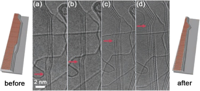
Figure 5. Edge motion of graphitic nanoribbons under Joule heating inside the transmission electron microscope. (a) A three-layer zigzag–armchair–zigzag–armchair edge array. The red arrow indicates the position of the zigzag–armchair edge junction at the beginning of the annealing process. After some time of Joule heating, the junction moves up ((b) and (c)), keeping the short zigzag-edge length almost unchanged. Eventually, the zigzag edge joins with the upper zigzag edge, forming a stable zigzag–zigzag–armchair edge array (d). Reprinted with permission from [62]. Copyright 2009 by the American Association for the Advancement of Science.
Download figure:
Standard image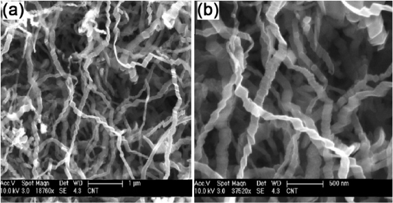
Figure 6. SEM images of CVD-grown carbon nanoribbons with different magnifications: (a) 1 µm scale, (b) 500 nm scale. Reprinted with permission from [63]. Copyright 2008 by Elsevier Ltd.
Download figure:
Standard imageInterestingly, GNRs could be fabricated using SiC tracks as a template [64, 65]. Sprinkle et al demonstrated the self-organized growth of GNRs with 40 nm widths on a template SiC substrate via scalable photolithography and microelectronics processing. Such as-grown GNRs can be used for the scalable fabrication of graphene devices, which exhibit quantum confinement at 4 K, an on/off ratio of 10 and a carrier mobility of up to 2700 cm2 V−1 s−1 at room temperature [64]. Robinson et al also demonstrated the direct synthesis of epitaxial GNRs by utilizing a crystallographic confinement technique unique to SiC. These authors discovered that the epitaxial growth of graphene initiates at the SiC step edge and consists of
 lattice planes, and multilayer graphene can form along a SiC terrace edge prior to on the formation of the terrace itself [65].
2.3.2. CVD of graphene sheets
In addition to the 'Scotch Tape' method used by Novoselov et al to obtain individual graphene layers [27], other researchers have reported alternative routes to synthesize graphene. One route deals with the growth of epitaxial graphite films by the thermal decomposition of SiC on the (0 0 0 1) surface [66]. An alternative method for producing single- and few-layered graphene uses the CVD process under ambient conditions on a polycrystalline Ni substrate [67]. This technique was modified using different carbon sources (e.g. polymer films and small molecules deposited on a catalytic metal substrate) [68]. Large-area graphene sheets have also been reported by Ruoff and co-workers using CVD with CH4 and H2 source gas mixtures at 1000 °C impinging on Cu foils [69]. Although these techniques are somewhat efficient, a challenge still persists: producing large amounts of graphene sheets, unattached to a substrate. To produce such a material, additional experimental work is required. For example, the use of other substrates, such as ZnS during the CVD of CH4 at 750 °C has been reported, and further acid treatments to dissolve the ZnS ribbons produced few-layer graphene nanoribbons (FLGNRs) [70]. It may be possible that other ceramic compounds could lead to a simpler formation of graphene sheets but further fundamental investigations are required.
2.3.3. Chemical synthesis of graphitic nanoribbons
It has been possible to synthesize graphene by electrophoretic deposition of diamond nanoparticles on HOPG followed by heat treatment [71]. Using a similar method, Cançado et al were successful in producing graphene edges, which were characterized by Raman spectroscopy [72]. Dai's group appears to have been the first to produce GNRs by the sonochemical exfoliation of commercial graphite in the presence of dichloroethane and a polymer, and these ribbons were used to construct field-effect transistor (FET) devices [48].
Pure organic chemical routes have been used to synthesize GNRs by linking tetra- and hexa-phenylbenzenes via the Suzuki–Miyaura reaction [73]. These GNRs are highly soluble in organic solvents due to the introduction of branched alkyl side chains, which act as functional groups to solubilize the GNRs. The lengths of these ribbons were found to be 8–12 nm, and they can form both aligned monolayers, as well as crystallized monolayers from solution by π–π stacking. This appears to be the first bottom-up approach to producing GNRs with armchair edges. However, different variants of this reaction could lead to longer or branched nanoribbons. In addition, it seems that it is more likely to produce armchair edges rather than zigzag edges using this approach and further investigations are needed along this line (figure 7) [49]. Hydrothermal synthesis involving Teflon-lined autoclaves has been used to synthesize amorphous carbon nanoribbons. In particular, C6H6, Na and ferrocene were introduced in the hydrothermal reactor at 210 °C for 24 h [74]. Other alternative approaches to produce graphitic nanoribbons have consisted of collapsing CNTs [75–79].

Figure 7. Bottom-up fabrication of GNRs. (a) Reaction scheme of chevron-type GNRs from tetraphenyl-triphenylene monomers. (b) STM image of chevron-type GNRs fabricated on a Au(1 1 1) surface (T = 35 K, U = −2 V, I = 0.02 nA). The inset shows a high-resolution STM image (T = 77 K, U = −2 V, I = 0.5 nA). (c) STM image of straight GNRs from bianthryl monomers after cyclodehydrogenation at 400 °C. The inset shows a higher resolution STM image. (d) High-resolution STM image with partly overlaid molecular model (blue) of the ribbon. Reprinted with permission from [49]. Copyright 2010 by Nature Publishing Group.
Download figure:
Standard image2.3.4. Graphene nanoribbons by unzipping carbon nanotubes
A natural source of GNRs is CNTs. By unzipping them, one could obtain single- and few-layered nanoribbons (figure 8). This unzipping technique was first developed in 2009 by several groups [37, 55, 80–82]. One of the methods, shown in figure 8(a), is based upon the intercalation of lithium in liquid ammonia into MWCNTs [37], followed by acid and thermal exfoliation treatments. Further improvements of this technique should be developed in order to obtain a complete unzipping of the tubes. The group led by James Tour [80] reported a chemical route based on the partial oxidation of MWCNTs using H2SO4 and KMnO4 (figure 8(b)). These nanoribbons exhibit oxidized edges, which make them highly soluble in polar solvents. More recently, Dai and collaborators reported an additional chemical method for unzipping CNTs by treating MWCNTs in air at 500 °C followed by the sonication of the resulting material in a 1,2-dichloroethane (DCE) organic solution of poly(m-phenylenevinylene-co-2,5-dioctoxy-p-phenylenevinylene) (PmPV) [83]. The catalytic cutting of graphene planes has become an attractive method (figure 8(c)) when compared with other chemical methods. Unfortunately, the amount of nanoribbons produced by this technique is approximately 5% of the starting CNT sample. In the past, various researchers have demonstrated that catalytic metal particles (e.g. Co, Ni, Fe) can cut graphene layers only along armchair or zigzag atomic directions [84–86]. Therefore, if metal nanoparticles are deposited on the surface of MWCNTs and these coated tubes are subsequently placed on Si wafers and treated at 850 °C, under a low flow of H2–Ar, the resulting material should consist of unzipped CNTs. This unzipping process consists of the metal catalyst dissociating carbon bonds, and these unbonded carbon atoms then react with H2 to form CH4 [87]. This route was successful in the unzipping of MWCNTs and N-doped MWCNTs [81]. In addition, it was also demonstrated that nanotubes could be easily unzipped by passing high electrical current inside a transmission electron microscope (figure 8(d)) [82]. An alternative method was recently developed by Dai's group. Their method consisted of embedding MWCNTs in poly(methyl methacrylate), subsequently turning the MWCNT composite over and the tubes that were not covered by the polymer were etched away by an Ar plasma (figure 8(e)) [55]. Various challenges still remain in controlling the nanotube opening processes, whether this opening occurs by exfoliation, etching, reduction or oxidation. In addition to challenges in controlling the opening of MWCNTs, a scalable process would have to provide conditions that prevent the agglomeration, wrinkling and entanglement of the produced nanoribbons, the entanglement being caused by attractive van der Waals forces which attract nanotube fragments. Finally, the unzipping of tubes preserving atomically smooth edges is still a challenge. Although a few groups have succeeded in observing atomically smooth edges in GNRs, more control on the edge morphology is still needed.
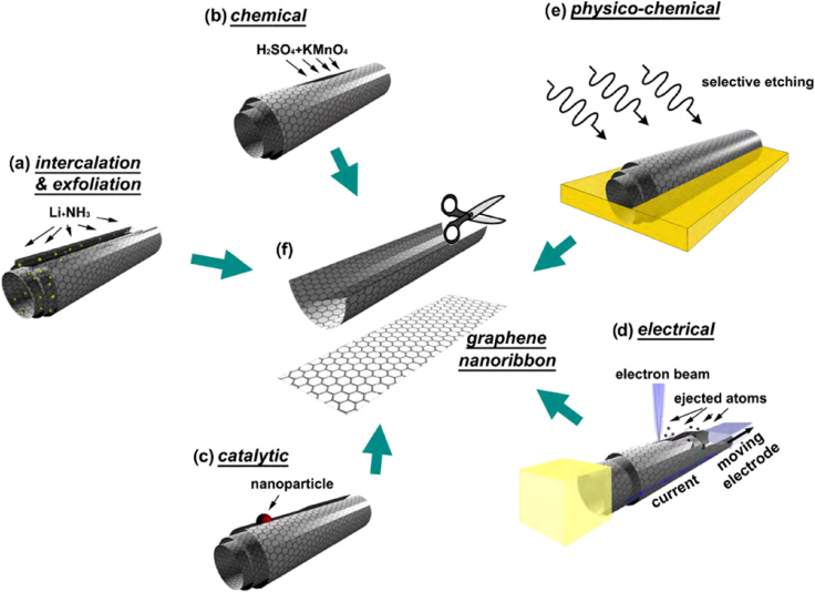
Figure 8. Unzipping CNTs into GNRs. (a) Intercalation-exfoliation of MWCNTs, involving treatments in liquid NH3 and Li, and subsequent exfoliation using HCl and heat treatments, (b) a chemical route involving acid reactions that start to break carbon–carbon bonds (e.g. using H2SO4 and KMnO4 as oxidizing agents), (c) a catalytic approach, in which metal nanoparticles 'cut' the nanotube longitudinally like a pair of scissors, (d) an electrical method by passing an electric current through a nanotube and (e) a physicochemical method by embedding the tubes in a polymer matrix followed by Ar plasma treatment. The resulting structures are either GNRs or graphene sheets (f). Reprinted with permission from [42]. Copyright 2010 by Elsevier Ltd.
Download figure:
Standard image2.4. Graphene as a substrate
A single layer of graphene has been shown to enhance the observed Raman signal of another sp2 hybridized carbon material placed on top of a graphene monolayer. In particular, the sp2 hybridized carbon sample could be another graphene layer, a CNT or a graphene ribbon [88, 89]. Figure 9(a) shows a schematic illustration of molecules on graphene [88, 89]. The Raman signal can be enhanced for each feature of an sp2 carbon sitting on a graphene layer when taking a Raman spectrum, and this effect has been called GERS, denoting graphene enhanced Raman spectroscopy, inspired by the surface-enhanced Raman scattering (SERS) process but produced by a different mechanism. A typical Raman-fluorescence spectrum of rhodamine 6G (R6G) in solution using 514 nm laser excitation is shown in figure 9(b) (the blue line). In contrast, for R6G adsorbed on graphene, the fluorescence emission could be effectively suppressed by a monolayer graphene substrate so that the Raman peaks of R6G are clearly observed (red line in figure 9(b)). As a reminder, the SERS process produces enhancements of Raman signals by many orders of magnitude when a sample sits on small highly faceted Ag nanoparticles, due to the interaction of the sample with the very strong electromagnetic field gradients produced by these tiny Ag nanoparticles. In the GERS process the signal enhancement is only about an order of magnitude, but it is expected that the GERS enhancement effect is reproducible and can be used as a more quantitative characterization technique than SERS. Therefore it is expected that the GERS effect should be useful to study the Raman spectra of defects sensitively. The use of gates to apply negative and positive voltages, and the use of different masses for 12C and 13C, are also helpful for studying Fermi level-dependent effects and to distinguish one carbon layer from another [90]. Although the SERS technique has been studied for more than 30 years [91], the exact nature of SERS is still debated. Using graphene as a substrate and then depositing some Au dots onto it, Novoselov's group has demonstrated significant SERS enhancements at 633 nm laser excitation and has studied the physics of SERS (figures 9(c) and (d)) [92]. It is found that three issues are crucial for further improvements of SERS: (1) a larger density of nanoparticle coverage, (2) a larger Mie enhancement and (3) a smaller nanoparticle–graphene separation. In particular, thin metallic nanodiscs will achieve the highest SERS enhancement for 2D systems like graphene [92].

Figure 9. Graphene as a substrate for enhanced Raman spectroscopy. (a) Schematic illustration of the molecules on a graphene/SiO2/Si substrate. Reprinted with permission from [88]. Copyright 2010 by the American Chemical Society. (b) Raman-fluorescence spectra of rhodamine 6G (R6G) in water (10µm) (blue line) and R6G on monolayer graphene (red line) at 514 nm excitation. Reprinted with permission from [93]. Copyright 2009 by the American Chemical Society. (c) SEM images of a graphene surface-enhanced Raman scattering (SERS) sample. (d) Representative Raman spectra measured across a line scan moving from the outside to the inside at the Au dot patterned area using 633 nm laser excitation. SLG denotes single-layer graphene and dots refer to gold quantum dots. An enhancement of all Raman peaks can be seen. Reprinted with permission from [92]. Copyright 2010 by the American Chemical Society.
Download figure:
Standard image3. Vacancies in graphene and graphene nanoribbons
HRTEM has been a valuable tool to study and generate defects, and to monitor structural reconstructions in carbon nanostructures [94–96]. Iijima and co-workers showed experimental evidence of vacancies and heptagon–pentagon pairs in SWCNTs and nanohorns (see figures 10(a) and (b)) [97]. Banhart and Krasheninnikov have reviewed, theoretically and experimentally, how the electron beam of a transmission electron microscope interacts with carbon nanostructures, thus changing their morphology via the generation, migration and reconstruction of defects (see figure 10(b)) [98].
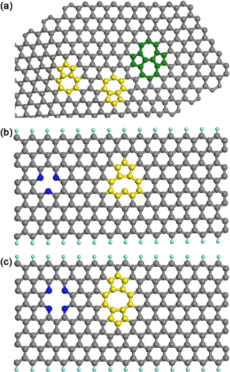
Figure 10. (a) Graphene patch with two separated 5–7 defects (yellow) and a Thrower–Stone–Wales defect (green) which can be formed by a pair of 5–7 defects. Molecular models of vacancy-type defects. (b) A vacancy and its reconstruction in graphene or in a GNR shown in blue could be reconstructed to save energy so as to form a pentagon and a defect with a dangling bond (atoms in yellow). Therefore, the reconstructed vacancy is more stable than the non-reconstructed case, which exhibits three dangling bonds. (c) Di-vacancy reconstruction in 2D graphene or in a GNR: a di-vacancy shown in blue could be reconstructed to form a pentagon–octagon–pentagon (5–8–5) defect shown in yellow with no-dangling bonds, therefore, the (5–8–5) defect being more stable.
Download figure:
Standard imageWith the latest technological improvements of HRTEM instrumentation, scientists are now operating transmission electron microscopes at lower accelerating voltages with atomic resolution, thus avoiding electron radiation damage in carbon samples. Using an aberration-corrected (AC-HRTEM) instrument operating at voltages of 80 keV, graphene could be characterized and also graphene defects could be visualized, allowing the detailed study of mono- and di-vacancies [99], heptagon–pentagon (7–5 pairs, Thrower–Stone–Wales defects (5–7–7–5), stacking faults and in situ reconstructions forming single carbon chains [100–104].
Molecular dynamics computer simulations and first-principles calculations of ion irradiation over graphene have demonstrated that ion irradiation can produce vacancies, di-vacancies, tri-vacancies and Thrower–Stone–Wales defects [105]. When considering a perfect graphene lattice, every atom is coordinated to three other carbon atoms and every edge is shared by two faces. If an even number of carbon atoms is removed, dangling bonds could be healed in order to preserve the carbon connectivity. However, if the number of vacancies is odd, there will be dangling bonds that make the structure more unstable and more chemically active. These reactive sites could subsequently be doped with foreign atoms, thus improving the specificity of the dangling bonds for binding other molecules. From a di-vacancy reconstruction, a 5–8–5 topological defect with no-dangling bonds (which is discussed in section 4.2) is the most energetically favored (see figure 10(c)) [105]. Therefore, if vacancies or reconstructed regions are generated (with an electron beam from a TEM microscope, for example) in an ordered way, these sites could be used to functionalize graphene with different atoms or molecules in a controlled manner for building specific sensor devices.
Although it is thought that magnetism is exclusively reserved for atoms with 3d or 4f electrons such as transition metals, it has been reported that vacancies induced by proton irradiation in graphitic systems could also be responsible for magnetism in carbon [106]. Density functional theory (DFT) calculations have shown that magnetism is possible in irradiated graphite [107]. Using magnetic force microscopy, Červenka and colleagues reported magnetic order in defective HOPG: the magnetism might be due to the arrangements of vacancies [108]. Ugeda and colleagues have studied the role of vacancies as the source of magnetism in carbon [109]. Recently, it has also been demonstrated experimentally that vacancies in graphene generate local magnetic moments which interact with the conduction electrons through the Kondo effect, thus generating magnetism in graphene [110].
Edges could also produce magnetism in graphitic nanoribbons: in 2000 Enoki and colleagues found that the magnetic behavior of a sample of activated carbon was due to the magnetic edge states of GNRs arranged in a disordered way [111]. Magnetic edge states have also been found in graphitic nanoribbons prepared by CVD [112]. The ferrimagnetic properties of nanographene networks caused by the electronic edge states have been studied by electron spin resonance (ESR) [113]. More recently, the role of dangling bonds and edge states in the magnetic properties of pristine and fluorinated graphene has been analyzed by near edge x-ray absorption fine structure (NEXAFS) [114]. Although some progress has been achieved in studying magnetic carbon, the role of vacancies and their controlled formation need to be better understood, and further experimental and characterization techniques also need to be developed.
3.1. Experimental generation of vacancies
In order to generate vacancies (di-vacancies, or larger vacancy clusters) in graphite or graphene in a controlled manner, the radiation damage by different energetic particles, such as electrons, protons or ions, on the carbon nuclei, should be further investigated. Thus, if the kinetic energy transferred to the nuclei is greater than a threshold value for bond-breaking, the carbon nucleus would be displaced in a sub-picosecond time scale generating a vacancy (knock-on displacement): for sp2 hybridized carbon atoms arranged in a graphitic lattice, the energy required to displace a carbon atom is between 15 and 20 eV [115]. Knock-on displacements could be achieved within a transmission electron microscope, since the electrons can acquire energies up to 300 keV, which is a large enough energy to displace carbon atoms [98, 115]. Therefore, TEM can be used to experimentally produce vacancies in a controlled fashion within carbon nanostructures. In fact, using TEM on SWCNTs, coalescence and covalent connections between the tubes could be achieved, thus producing a novel type of nanostructure different from the originally irradiated precursor. In these cases, the vacancies are responsible for merging the nanotubes due to the high reactivity of the dangling bonds that are produced [95, 116]. Other TEM experiments for reducing an MWCNT diameter via controlled vacancy introduction have been performed [117]. In fact, TEM-induced vacancies have been used to connect the atomic planes of MWCNTs with metallic nanoparticles [118]. Banhart's group has used the electron beam of a transmission electron microscope to create vacancies in double-layer graphene to trap metal atoms or metallic clusters [119]. In this context, it could be envisaged to use the transmission electron microscope to connect graphene with metals generating an almost perfect contact, similar to metal–nanotube covalent junctions [118].
In addition to the use of protons as mentioned above [106], another technique to produce vacancies in graphitic systems involves the use of different types of ions. Ney and colleagues have irradiated graphene flakes with 100 keV nitrogen ions and they performed magnetic measurements at 5 K finding that the paramagnetism originally measured (probably due to edge states) increases up to doses of 1015 ions cm−2 and then decreases for higher doses due to the amorphization of the graphene. These authors did not find ferromagnetism; however, the nature of the defects that were generated has not been addressed and the role of the nitrogen implanted atoms would need further studies in order to understand how nitrogen interacts with carbon [120]. Probably for this case, the vacancies generated by nitrogen involve the ejection of several carbon atoms, thereby producing large regions of dangling bonds in a disordered way. Certainly, one of the challenges for the future is the generation of vacancies of different sizes (mono-vacancy, di-vacancy, etc) and the identification of their precise location on the hexagonal lattice in an automated way.
3.2. Calculations of vacancies in graphene and graphene nanoribbons
According to tight-binding molecular dynamics and Monte Carlo simulations, vacancies trigger the coalescence mechanism of SWCNTs observed under TEM [95]. Without the vacancies generated by the electron beam, the graphene sheets that form the SWCNTs could not interact and thus could not merge the tubes. First-principles DFT calculations with the Perdew, Burke and Ernzerhof (PBE) approximation exchange-correlation density functional have been used to simulate defect formation in graphite by assuming an initial transfer of momentum to the carbon atoms. The results show that vacancies, interstitials and Thrower–Stone–Wales-type defects are indeed possible, and exhibit formation energies ranging between 5 and 15 eV [121].
Most of the calculations on vacancies in graphite and graphene show a magnetic behavior. Using spin-polarized DFT in graphite, Lahtinen and colleagues simulated the differences in magnetic behavior between a vacancy and a hydrogen-vacancy defect showing that the presence of hydrogen in the vacancy makes the local magnetic moment increase to double its magnitude when compared with the naked vacancy case [107]. In this context, vacancy and hydrogen adsorption-induced magnetism has been studied by first-principles simulations showing that the ferromagnetism and antiferromagnetism depends on whether the defects belong to the same sublattice or not [122]. The mean field Hubbard model has been used to study theoretically the different magnetic properties that vacancies and voids (in which more than one atom is removed from the graphene lattice) exhibit in graphene and GNRs, finding that there is a rich spectrum of possible behaviors, depending on the spatial arrangement of the defects and their sublattice imbalance [123]. Yazyev concludes that only single-atom defects, such as vacancies or chemical functionalizations, that are unevenly distributed in the two graphene sublattices, can produce a net magnetic moment [124]. Bao and colleagues have studied theoretically the magnetic properties of tetra-vacancies in graphene and also such vacancies saturated with hydrogen. They found that the tetravacancy reconstructs by relaxation and the magnetic moment is lost; however, when the tetravacancy is saturated with hydrogen, there is a magnetic moment [125]. Cui et al have studied with spin-polarized DFT different size-vacancies or voids which the authors call nanoholes. They have found a remarkable stability for certain size nanoholes with the number of atoms thus removed called magic numbers. A large number of the nanoholes studied exhibit a magnetic state with a finite energy band gap [126].
4. Topological defects
In the context of graphene and graphene-like nanostructures, including fullerenes, nanotubes and schwarzites, a topological defect does not change the connectivity of the sp2 lattice, that is, every carbon atom in the structure has exactly three nearest neighbors, even though, their physicochemical properties do change. Generally speaking, these defects can change the curvature of the system locally or globally. In this review, since planar graphitic nanostructures are studied (graphene and nanoribbons), we will deal with those topological defects that do not change the curvature globally; these include heptagon–pentagon dislocations, Thrower–Stone–Wales transformations, double pentagon–octagon (5–8–5), double pentagon–heptagon (D5D7), triple pentagon–heptagon (T5T7) cluster defects, grain boundaries and extended line of defects.
4.1. Heptagon–pentagon pairs and the Thrower–Stone–Wales transformation in graphene and nanoribbons
In 1969, Peter Thrower, when he studied dislocations in graphite, introduced the possibility of having a pentagon'–heptagon defects in a graphitic lattice (see figures 10(a) and 11(a)) [127] as a stable nano-cluster. However, not much progress in this area was made until the appearance of fullerenes in 1985. Fullerenes, graphene, schwarzites and CNTs are locally similar in the sense that every carbon atom is connected to three other carbon atoms (sp2 character). With this line of reasoning in mind, some of the mechanisms that apply to fullerenes could also be valid for CNTs and graphene. This is the case of the bond rotation proposed by Stone and Wales in 1986, and applied to Buckminsterfullerene C60(Ih symmetry) to transform it into another isomer with different symmetry (C2v) by rotating one bond by 90° (see figure 11(b)) [128]. Therefore, based on the fact that Peter Thrower proposed the existence of pentagon–heptagon defects and that Stone and Wales studied 90° bond rotations in fullerenes, which produce heptagon–pentagon pairs in graphene, we will refer to this bond rotation as the TSW transformation (Thrower–Stone–Wales transformation) (see figure 11(c)). Geometrically, the main effect of the TSW transformation in fullerenes, CNTs and graphene is a change to the local environment, but preserving the connectivity while producing no-dangling bonds. The TSW transformation is a matter of study in graphene, nanotubes, schwarzites and graphitic onions: by applying the TSW transformation to giant fullerenes, the sphericity and stability of giant graphitic onions could also be explained [129–131].
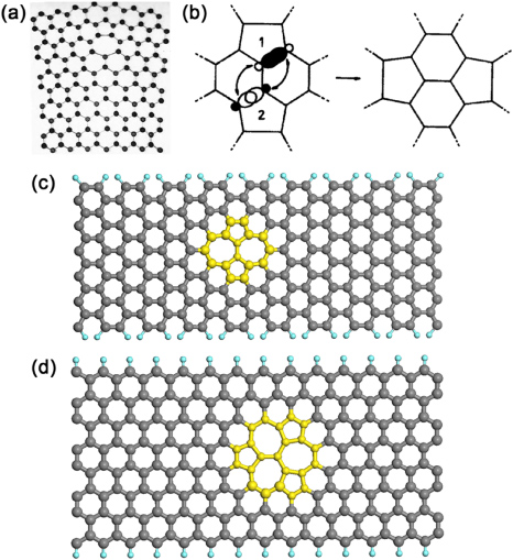
Figure 11. (a) Original Thrower stick-ball model of a 5–7 defect [127]. (b) Original Stone and Wales drawing of the bond rotation changing the symmetry of C60 from Ih to C2v. Reprinted with permission from [128]. Copyright 2010 by Elsevier Ltd. (c) Thrower–Stone–Wales (TSW)-type defect obtained by rotating one of the bonds in a ZGNR by 90°. This defect consists of two 5–7 defects joined together. (d) Triple five–triple seven (T5T7) defect depicted in a GNR.
Download figure:
Standard imageCrespi and co-workers applied the TSW transformation to graphene in order to modify the hexagonal honeycomb lattice to form another lattice with only heptagons and pentagons (also known as pentaheptite), which had a metallic character and exhibited a large density of states at the Fermi level [132]. Terrones et al took this idea further by having three 2D graphene-like systems with hexagons, heptagons and pentagons, in an ordered way: these crystal structures were called Haeckelites in honor of Ernst Haeckel, a famous German zoologist and biologist (1834–1919) who drew the first radialoria models with such topological similarities to graphene and fullerenes. The Haeckelites also exhibit states at the Fermi level and have high energetic stability [116]. The transport and vibrational properties of Haeckelites have also been studied by first-principles calculations [133]. Different families of Haeckelites have been proposed theoretically, and their electronic and mechanical properties have been studied [134–136]. However, so far Haeckelites remain an experimental challenge and have not been synthesized in the laboratory. Graphene reconstruction producing heptagons and pentagons to preserve the structural connectivity has been reported and TSW-type defects have also been identified in these systems [137, 138]. Using aberration-corrected high-resolution transmission electron microscopy (AC-HRTEM) and STM techniques, 5–7 and TSW defects on isolated graphene surfaces could be directly observed. Some recent experimental evidence, at the atomic scale, of several types of defects in graphene obtained by different research groups [100, 101, 138–140] are depicted in figure 12.
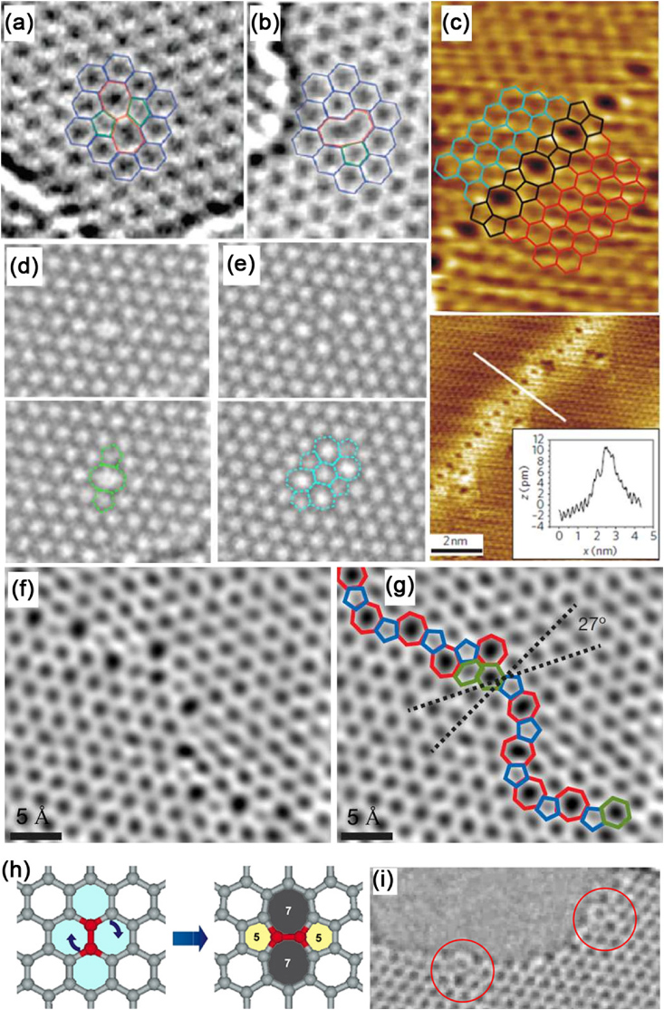
Figure 12. (a) TEM image of a TSW defect (55–77), formed by rotating a carbon–carbon bond by 90° and (b) a single vacancy as seen in an experimental TEM image. Reprinted with permission from [100]. Copyright 2008 by the American Chemical Society. (c) Top image: defect structure and superimposed defect model. Bottom image: line defect with image profile in the direction perpendicular to the wire (inset). The brighter area surrounding the defect originates from the states with wave functions localized at the defect. Reprinted with permission from [139]. Copyright 2010 by Nature Publishing Group. (d) Top images: TEM image of a di-vacancy (V2 (5–8–5)) and (e) image V2(5555–6–7777) di-vacancy. Bottom images: corresponding images of the defects shown in the top images of (d) and (e) in which the defects have been drawn in color for better identification. Reprinted with permission from [138]. Copyright 2011 by the American Physical Society. (f) Two grains (bottom left, top right images) intersect with a 27° relative rotation. An aperiodic line of defects stitches the two grains together. The image from (g) with the pentagons (blue), heptagons (red) and distorted hexagons (green) of the grain boundary are outlined. Reprinted with permission from [140]. Copyright 2011 by Nature Publishing Group. (h) Molecular model showing the transformation of four adjacent hexagons into a 5–7–7–5 defect or a TSW defect, and (i) AC-HRTEM images showing two 5–7–7–5 defects located on the edges (red circles) of a hole in a graphene surface (images taken from movie supplementary material of [101]. Copyright 2009 by the American Association for the Advancement of Science).
Download figure:
Standard image4.1.1. Experimental evidence and characterization of topological defects in graphene and graphene nanoribbons
As we have mentioned in section 3 devoted to vacancies, HRTEM is an ideal tool to visualize, generate and study defects in situ in graphene-like lattices. TSW defects and carbon rings with more than seven atoms, and their dynamics under the electron beam have been characterized with HRTEM in SWCNTs that were previously heated [141]. Regarding graphene, the formation and annealing of TSW defects has been observed in situ using AC-HRTEM with a monochromator working at acceleration voltages of 80 keV; further, also in these observations defects exhibiting three heptagons and three pentagons or the T5T7 defect (denotes triple five–triple seven) were identified [100] (see figure 11(d)); T5T7 defects can be generated experimentally by a divancy reconstruction [142].
Raman spectra exhibit a blue shift during the oxidation and exfoliation of graphite which was thought to be caused by the presence of TSW defects or 5–8–5 defects. However, Kudin and colleagues have demonstrated that although these defects exhibit particular features worth studying, most probably the observed Raman shift was caused by an alternation of single–double carbon bonds within the sp2 hybridized carbon ribbon, which could be due to the presence of sp3 hybridized carbon atoms on the edges of zigzag nanoribbons [143]. The generation and study of T5T7 defects in graphene has been carried out experimentally using HRTEM. In this in situ observation, tungsten atoms can be trapped by this defect [144]. First-principles calculations show that among several possible defects, such as single vacancies, di-vacancies (5–8–5) and the TSW, it was the T5T7 defect that was the one that could explain the experimental observations [144].
Certainly, HRTEM offers advantages over other techniques to characterize and generate topological defects in graphene-like structures. However, other tools which are gaining importance are STM, STS and Raman spectroscopy. Nevertheless, to gain a better understanding of the different types of defects, new tools and combinations of tools to characterize defects more quantitatively are needed in order to establish a robust defect engineering strategy for applications.
4.1.2. Theoretical studies of topological defects in graphene and graphene nanoribbons
As has been shown experimentally and theoretically by Cretu and colleagues in the previous section [144], topological defects are more reactive and could be used to trap atoms or molecules with different strengths depending on the defect geometry. In this context, Duplock and colleagues have studied theoretically the role of TSW defects in attracting hydrogen and finding that certainly this type of defect makes H2 chemisorption thermodynamically favorable [145].
Study of the diffusion, coalescence and reconstruction of defects is crucial in order to shed light on the stability of specific defects: Lee and co-workers have used tight-binding molecular dynamics and first-principles calculations to demonstrate that two single vacancies coalesce to form a 5–8–5 defect, and by heating, this is transformed into a T5T7 defect via a TSW transformation [146]. In addition, these authors have found that four single vacancies coalesce to form a double T5T7 defect which is the basic defect in the hexagonal Haeckelite structure proposed by Terrones et al [116]. The stability of T5T7 defects against a pair of 5–7 dislocation defects has been compared using first-principles calculations, and it is found that two 5–7 pairs, separated by a distance determined by the reconstruction of ten vacancies (around 7.32 Å), are more stable than a patch of five T5T7 defects tightly packed in a graphene lattice (five T5T7 defects can be generated by ten vacancies) [147].
Topological defects in graphene have also attracted the attention of scientists working in other fields, for example, the continuum theory of elasticity has been used to study interactions of TSW defects in graphene and also the properties of 5–8–5 defects and the results of continuum theory were found to agree with the results using atomistic methods [148, 149]. In addition, using a cosmological analogy, Cortijo and co-workers have coupled the Dirac equation to a curved space to study topological defects in graphene [150].
STM and STS provide information on the different types of defects, including the local density of states (LDOS), since the electronic behavior at the defects is different from electrons in the normal graphene lattice: Amara and colleagues have simulated, using tight-binding calculations with the Tersoff–Hamann approach [151], the STM images from vacancies, 5–8–5 defects, adatoms and TSW defects [152]. This information is valuable and useful to experimentalists for comparisons with experimental TEM and STM images.
Topological defects can also be seen as centers for chemical activity, so their functionalization is relevant for graphene nanoelectronics. Boukhvalov and Katsnelson have used hydrogen to test theoretically the chemical properties of graphene with topological defects such as TSW and 5–8–5 defects [153]. The chemical functionalization by carboxyl groups (COOH) of semiconducting GNRs possessing TSW defects has been studied using first-principles calculations, finding that the electrical conductivity could be enhanced by mono- and double-adsorption of COOH at the TSW defects. Therefore, the conductivity depends on the capability of adsorbing the COOH groups by the TSW defects; having a higher concentration of TSW defects augments the adsorbing sites which can be functionalized by COOH, transforming the semiconducting nanoribbon into a p-type metallic system [154].
Thermal transport in graphene zigzag nanoribbons with TSW defects has also been studied using the non-equilibrium Green's function method and the phonon-wave packet scattering method. The results demonstrate two unique thermal transport phenomena: an edge localized thermal current at low energies and a circulating thermal current along the heptagonal ring of the TSW defect [155].
Although stress and mechanical stability are usually studied by classical methods, at the nanoscale, quantum effects also occur. Huang and colleagues have studied the stress at the edges in AGNRs and ZGNRs using first-principles methods, finding quantum effects: for AGNRs the stress oscillates with the ribbon width, and for ZGNRs the edge stress is small and exhibits a very weak width dependence; moreover, the edge stress in ZGNRs is further reduced in antiferromagnetic nanoribbons (ground state) compared with the paramagnetic case. These effects cause twisting and wrapping mechanical instabilities in the nanoribbon which cannot be explained by continuum or empirical approaches [156]. The authors also show that hydrogen passivation at the edges of both AGNRs and ZGNRS relieves the edge stress caused by dangling bonds. In this context, other atoms or molecules could be added at the edges (instead of hydrogen) to relieve the edge stress. In addition, according to these authors [155], TSW edge reconstructions reduce the mechanical instability and improve the chemical stability of the GNRs.
In addition to vacancies, topological defects can also alter the two graphene triangular sublattices producing different magnetic effects, depending on the type of defect. In this context, López-Sancho and co-workers have used the Hubbard model to study the magnetic effects caused by the presence of heptagons, pentagons, heptagon–pentagon dislocations and TSW defects [157]. With DFT and quantum Monte Carlo calculations, the long range effects of TSW defects in graphene have been studied [158]. It turns out that TSW defects distort the graphene lattice, causing adjacent atoms to move out of the plane, thus producing ripples in the graphene sheet. However, the rippling or buckling behavior of graphene with several TSWs or other types of topological defects needs to be studied in depth. For the case of Heackelites, depending on their geometry, there will be a certain local wrinkle in the sheets, that is, some atoms will protrude out of the sheet plane [116].
Quantum transport of ZGNRs has also been studied with first-principles calculations: the results indicate that ZGNRs which are mirror symmetric with respect to the midplane between edges, exhibit small currents with the presence of a conductance gap around the Fermi level, whereas non-symmetric ZGNRs possess a linear current–voltage ohmic behavior [159]. However, when including spin polarization in the transport calculations, both types of ZGNRs (symmetric and non-symmetric) are semiconductors, but for the symmetric cases, negative differential resistance is observed in the I–V curves [160]. If a TSW defect is inserted into ZGNRs, the asymmetric ZGNRs exhibit lower currents in their I–V curves but with a similar behavior as is seen in the perfect ZGNRs. For symmetric ZGNRs with a TSW defect, strong differences in the currents with different spin polarizations appear, and the negative differential resistance is reduced [160]. Although transport measurements have been carried out in GNRs obtained from chemical methods (edges of these GNRs are not atomically smooth), the GNRs are found to be semiconductors [48]. So far the effect of topological defects has not been measured experimentally.
The reactivity of topological defects at the edges of ZGNRs has been studied with first-principles calculations to explain the loop formation at the edges in Joule heated nanoribbons [62, 161]. It is has been shown that when a ZGNR is previously irradiated with an electron beam, the edges reconstruct via topological defects such as pentagon–heptagon pairs called 'reczag' edges, which do not interact, or they interact very little with the layers above and below, thus avoiding loop formation. Without the presence of these defects, the loops can also be formed by Joule heating at the edges of ZGNRs [161]. The observed dynamics of di-vacancies by Girit and co-workers under the HRTEM [101] has been studied theoretically with a first-principles approach in order to explain the migration, rotation and transformation of 5–8–5 and T5T7 defects [162].
4.2. Grain boundaries and an extended line of defects in graphene and nanoribbons
As stated in the first section of this review, Roscoe and Thomas proposed a model for small angle grain boundaries in graphite, from which it is possible to identify the presence of pentagon–heptagon pairs, although for some reason they did not draw the bonding in this regions [7, 10] (see figure 1(b)). Almost three decades later, Terrones and Mackay, using the concept of curvature in graphitic systems, introduced a twin boundary in graphene using pentagons and heptagons (see figures 13(a) and (b)) [163].
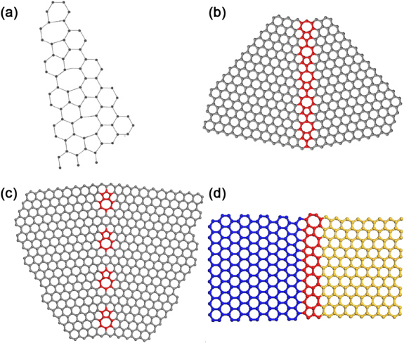
Figure 13. (a) Original drawing by Terrones and Mackay of a graphene grain boundary with heptagons and pentagons (5–7) defects joined together. Reprinted with permission from [163]. Copyright 1992 by Elsevier Ltd. (b) Computer generated model of the boundary shown in (a), and the defect clusters are periodically separated by around 6.52 Å. (c) Graphene grain boundary in which the 5–7 defects are periodically separated by 11.55 Å. (d) Joining armchair (blue) and zigzag (yellow) nanoribbons by a line of 5–7 defects (red).
Download figure:
Standard imageExperimentally, in 1988 Albrecht and colleagues studied tilt boundaries in graphite with STM [164]. From these STM studies on HOPG and computer simulations, Simonis and co-workers proposed a grain boundary model which is similar to the one proposed by Terrones and Mackay in 1992 [165]. Pong et al used STM to characterize small angle grain boundaries in graphite: these authors proposed a model based on 5–7 dislocations separated periodically by a greater distance than the model proposed by Terrones and Mackay. By changing the separation of the 5–7 defects, the angle between the grains is also changed [166] (see figure 13(c)). Červenka and Flipse, used STS to characterize the electronic properties of grain boundaries in HOPG and found that the charge density at the boundaries was higher than that of graphite and that the charge density exhibits two strongly localized states [167]. In addition, ferromagnetic behavior at room temperature has been identified in grain boundaries of HOPG by magnetic force microscopy (MFM) and superconducting quantum interference device (SQUID) measurements [108].
Andriotis and Menon studied theoretically the transport properties of 'T-shape' GNRs exhibiting aligned 5–7 defects to connect AGNRs with ZGNRs, finding that the conductivity depended on the chirality, width and the 5–7 defects boundary [168]. Botello-Méndez et al, also using a 5–7 defect-boundary to join AGNRs with ZGNRs, studied the electronic and transport properties of hybrid GNRs and found that such nanoribbon structures exhibited half-metallicity; this means that electrons with spin of just one type, spin up or down, but not both, participate in the conduction. It is noteworthy that these hybrid nanoribbons possess a distortion of the graphene lattice which might affect their stability and their potential use for spintronics applications (see figure 13(d)) [169].
Electronic properties, stability and STM simulations of different angle grain boundaries in graphene have been studied with first-principles calculations to show the differences between small angle and large angle grain boundaries. Small angle grain boundaries have a tendency to produce buckling of the graphene sheet [170]. Quantum transport has also been studied theoretically, showing that depending on the boundary, two behaviors are present: high transparency of charge carriers and perfect reflection [171].
More recently, Lahiri et al [139] found that by growing graphene on nickel [111] one could produce an extended line of defects (ELD) involving 5–8–5 defects arranged in a periodic way. Using STM, the authors found that the image contrast is brighter in the vicinity of the defect, thus corresponding to the electronic states with wavefunctions localized at this specific region. The same authors performed first-principles calculations, demonstrating that the ELD 5–8–5 behaves as a nanowire embedded in a graphene lattice since this defect produces electronic states at the Fermi level, and these states extend along the defect. In fact, this ELD 5–8–5 could be observed in two graphene grains, with zigzag edges, joined together by a pair of atoms arranged periodically (see figure 13(d)). Kou et al found, using the local spin density approximation, that there is a small magnetic moment of around 0.03μB per cell which can increase up to 0.7μB per cell under strain [172]. As expected, the spin polarization is localized ferromagnetically along the ELD 5–8–5 line.
Botello-Mendez et al used local density approximation and general gradient approximation (GGA) calculations to study different extended lines of defects in graphene and GNRs involving heptagons, octagons and pentagons (5–8–5 defect, D5D7 defect and T5T5 defect (see figure 14, [142]). The calculations reveal that all these ELDs compete in energy and that when nanoribbons possessing these ELDs are considered, stable ferromagnetic configurations might appear, in particular for the ELD T5T7 case [142]. These authors also simulated the STM images from first-principles calculations using the Tersoff–Hamann approach [151], and confirmed that indeed, the Lahiri ELD 5–8–5 defect corresponds to a structure involving pentagons and octagons. The transport properties were also calculated for these cases, finding that all ELDs should be observable in electron transport measurement. However, for the T5T7 case, there are extra conduction channels favoring electron conductance and magnetic properties [142].
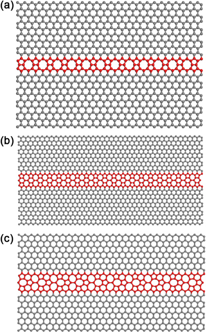
Figure 14. Molecular models of extended lines of defects: (a) 5–8–5 defects in a ZGNR, (b) double pentagon–double heptagon (D5D7) defects in a ZGNR and (c) triple pentagon–triple heptagon (T5T7) defects embedded in a ZGNR.
Download figure:
Standard image5. Doping and functionalization
Doping and functionalization with other atoms or molecules are efficient ways to modify the electrical properties of graphene. The doping of graphene could be roughly classified into two categories [173]. One is electrical doping by changing the gate voltages of graphene devices; another is chemical doping using chemical routes, such as substitutional doping or the controlled reduction of graphene oxide. It is noteworthy that the terminology 'doping' here is a little bit different from the one widely used in semiconductor physics. The substitutional heteroatoms (B, N, etc) in the graphene lattice sometimes can reach relatively high doping levels (2% or higher [174]). In this section, some recent progress in the chemical doping and functionalization of graphene and GNRs will be demonstrated and summarized. In addition, the importance of the dopant sites will be reviewed, and by changing a dopant, one could tailor the properties of graphene.
5.1. Substitutional doping of graphene with N, B, S, P, Si and reduced graphene oxide
As a single layer of a hexagonal lattice, graphene is constructed by sp2 hybridized carbon atoms, and three strong σ bonds are established with the other three surrounding atoms. The pz orbitals of these C atoms form a filled band of π orbitals (valence band) and an empty band of π * orbitals (conduction band) [173]. According to tight-binding calculations, the valence and conduction bands touch at the Brillouin zone (figure 15) [175], thus making graphene behave like a zero-band-gap semiconductor [39, 66]. However, for graphene applications in digital electronics, such as in FETs, it is highly desirable to open a band gap in graphene [176]. Many strategies, such as the substrate-induced method [177], the application of an electric field to bilayer graphene [178, 179] and the size confinement effect by forming GNRs [48], have been proposed to introduce an energy band gap. In addition to these possibilities, chemical modification of graphene, such as by substitutional doping with other atoms (e.g. N, B, P, S, etc) [174, 180, 181] or the controlled reduction of graphene oxide (GO) [182] could be effective routes to open a band gap in graphene. Furthermore, the chemical and electronic properties could be modulated in a well-controlled manner by adjusting the doping and reduction level in the two above-mentioned methods. In this subsection, some typical advances in the area of substitutional doping of graphene and reduced GO will be described.
Figure 15. The low-energy band structure of graphene. Reprinted with permission from [175]. Copyright 2011 by the American Physical Society.
Download figure:
Standard image5.1.1. Substitutional doping of graphene with N, B, S, P, Si
Thrower and co-workers have investigated the doping effect of heteroatoms (e.g. B, N, P) into carbon materials (e.g. graphite, carbon fibers), and these authors found that their properties could be remarkably tuned by substitutional doping [183–185]. For graphene, substitutional doping implies that the carbon atoms in the hexagonal lattice are substituted with dopants (e.g. N, B, P, S), whose incorporation into the lattice would disrupt the sp2 hybridization of the carbon atoms, and would cause significant changes to the electronic properties of graphene. Based on different substitutional sites, there are usually three kinds of ways of introducing N atoms within the hexagonal lattice, and these are substitutional graphitic nitrogen (N1), pyridine-like nitrogen (N2) and pyrrolic nitrogen (N3), as shown in figure 16.
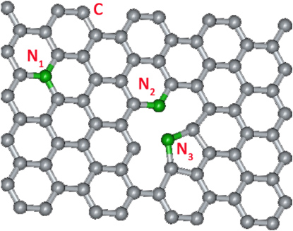
Figure 16. Molecular model showing the types of N doping in a graphene sheet, in which the gray and green atoms denote carbon (C) and nitrogen (N), respectively. The sites N1, N2 and N3 represent substitutional graphitic nitrogen, pyridine-like nitrogen and pyrrole-like nitrogen, respectively.
Download figure:
Standard imageDFT calculations on ZGNRs have demonstrated that the doping of N and B produces different effects, depending on the position of the substitutional sites [186]. In particular, edge substitutions at low density do not significantly alter the band gap, while bulk substitution promotes the onset of a semiconducting-metal transition. In addition, pyridine-like defects (at an N2 pyridinic site) induce a semiconducting-metal transition. The first experimental work on nitrogen-doped graphene (NG) was demonstrated using methane and ammonia as precursors in a CVD system [174]. It was found that N atoms can be substitutionally doped into the graphene lattice. Electrical measurements show that the NG exhibits an n-type electronic behavior, as demonstrated in figure 17. Furthermore, compared with pristine graphene (PG), NG shows a lower electrical conductivity and a larger on/off ratio. The room temperature mobilities of the PG and NG devices are about 300–1200 cm2 V−1 s−1 and 200–450 cm2 V−1 s−1, respectively [174]. Thus, the mobility of NG is about 1–2 orders of magnitude lower than that of mechanically exfoliated graphene (1.5 × 104 cm2 V−1 s−1) [27], and this lowered mobility might be attributed to carrier-defect scattering at the doping and topological defect sites. More importantly, the substitutional doping of nitrogen within a graphene lattice could form covalent bonding with carbon atoms, which would modify the electrical structure of graphene, and suppress the development of a high DOS of graphene near the Fermi energy level. Therefore, a gap could be opened between the valence and the conduction bands. Obtaining a controlled band gap is very meaningful for the possible future applications of graphene in semiconductor electronics.
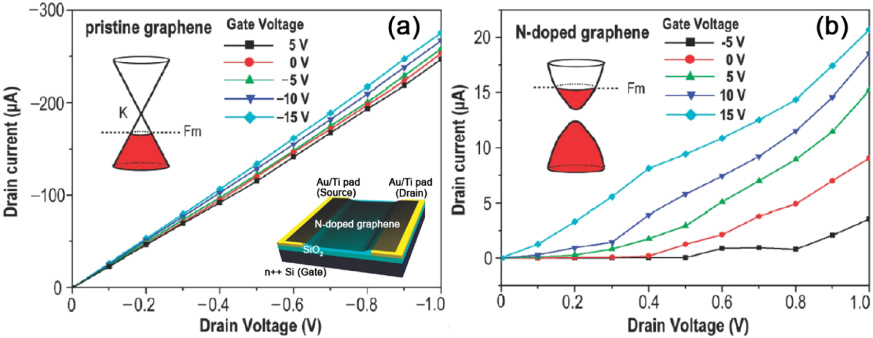
Figure 17. Electrical properties of N-doped graphene. (a), (b) Ids/Vds characteristics at various gate voltages Vg for the PG and the N-doped graphene FET device, respectively. Here Ids, Vds and Vg denote source–drain current, source–drain voltage and gate voltage, respectively. The upper-left insets in each panel are the presumed band structures. The lower-right inset in (a) is the schematic device configuration. Reprinted with permission from [174]. Copyright 2009 by the American Chemical Society.
Download figure:
Standard imageSome of the recent achievements related to NG synthesis are summarized in table 1. Except for ammonia (NH3) gas, some other nitrogen-containing liquid precursors, such as acetonitrile (CH3CN) [187], pyridine (C5H5N) [188, 189] or solid precursors, including cyanuric chloride (C3Cl3N3) [190], have also been used for the synthesis of NG with few-layers (usually no more than ten layers in thickness). Regarding the synthesis, as shown in table 1, the CVD method is the most common due to its advantages in achieving a relatively high crystallinity when compared with wet chemical methods. In addition, some post treatments on few-layer PG, such as Joule heating [180] and plasma treatment [191, 192], in nitrogen-containing gases (NH3, N2, etc) have been used for obtaining NG. These post-treatments have unique advantages in transistor fabrication, especially for batch device production.
Table 1. Summary of some experimental work on nitrogen-doped graphene (NG) synthesis.
| Layers | Method | Substrate | Precursors | Growth parameters | Reference |
|---|---|---|---|---|---|
| 2–6 | CVD | Cu (25 nm) film on silicon wafer | Methane (CH4) and ammonia (NH3) | 800 °C, 10 min | [174] |
| 2–8 | CVD | Ni (300 nm) film on silicon wafer | Methane (CH4) and ammonia (NH3) | 1000 °C, 5 min | [193] |
| ⩾1 | CVD | Cu foil (25 µm thick) | Acetonitrile (CH3CN) and ammonia (NH3) | 950 °C, 500 mTorr, 3–15 min | [187] |
| 1 | CVD | Cu foil (25 µm thick, 99.999%) | Pyridine vapor | 1000 °C, 10 min at ∼7 Torr | [188] |
| 1–2 | CVD | Cu foil (34 µm thick, 99.95%) | Ethylene (C2H4) and ammonia (NH3) | 900 °C, 4.6 Torr, 30 min | [194] |
| ⩾1 | CVD | Ni (300 nm) or Cu (300 nm) film on silicon wafer | Methane (CH4) and Ammonia (NH3) | 980 °C, 3 min (for Ni) or 20 min (for Cu) | [195] |
| 1–3 | Electrothermal reactions | Graphene nanoribbons on silicon wafer | Ammonia (NH3) | e-annealed graphene nanoribbons in NH3 | [180] |
| >2 | Arc discharge | No substrates | Graphite rod, pyridine vapor or ammonia (NH3) | Flowing H2 (200 Torr) and He (500 Torr) through a pyridine bubbler | [189] |
| 1–2 | Plasma post treatment | Pristine graphene | Ammonia (NH3) | NH3 plasma at a dose of 3 × 1014 cm−2 | [192] |
| >2 | Plasma post treatment | No substrates | Reduced graphene oxide and N2 | Treatment in nitrogen plasma (500 W power, 14 Torr N2) | [191] |
| >2 | Vacuum annealing | Ni (100–300 nm)/B (5–15 nm) films on silicon wafers | Boron-trapped nitrogen and nickel-trapped carbon atoms | 800–1100 °C, 60 min, 10−3–10−4 Pa | [196] |
| 1–6 | Solvothermal | No substrates | Lithium nitride, tetrachloromethane and cyanuric chloride | 250–350 °C, 6–10 h | [190] |
Theoretical calculations [43, 45] and experimental work [48, 197] have demonstrated that GNRs with narrow widths (<10 nm) and atomically smooth edges will exhibit band gaps useful for FETs operated at room-temperature. The GNR-derived FETs have demonstrated p-type behavior with excellent on/off ratios (∼107 at room temperature) [48]. By high-power electrical Joule heating of pristine GNR-FETs in ammonia gas, n-type FETs could be produced [180]. During electrical annealing, the more reactive carbon atoms at the edges of the GNRs could react with ammonia to form C–N bonds. The Dirac point shifts by about 20 V to negative gate voltages when compared with nanoribbons annealed by e-beam in vacuum, thus confirming the n-type doping effect of nitrogen atoms. In addition, the n-doping level was found to be approximately proportional to the density of substitutional N atoms in the GNR edges [180].
Substitutional doping with boron is another interesting way to modulate the electronic properties of graphene. Theoretical work has been carried out along this direction [181, 198–203]. In this context, DFT has demonstrated that substitutional boron atoms will act as scattering centers for the electronic transport along the GNRs (substitutional boron concentration is 1.4%) [181]. If the boron atoms are doped at the edges of ZGNRs, the B-doped ZGNRs may show half-metallic behavior, which gives rise to a zero band gap for electrons with one spin orientation and a semiconducting or insulating band gap for the other spin orientation, thereby giving rise to a completely spin-polarized current. The half-metallicity of B-doped ZGNRs does not depend on the ribbon width even in the absence of an electric field, and this property is preserved for any field strength. This demonstrates the possibility of using B-doped graphene for spintronics applications [203]. Figure 18(a) shows the structure schematically of B-doped bilayer graphene. Theoretical work by Menezes et al has demonstrated that pure bilayer graphene does not show a band gap (figure 18(b)), whereas if a disordered arrangement is imposed on only one of the sublattices (blue dotted line), a band gap (∼0.2 eV) opens up. However, when disorder is imposed upon both sublattices (upper and lower graphene sheets; red dashed line), the gap shrinks again and shifts to higher energy (figure 18(c)). This demonstrates that an energy-gap opening of bilayer graphene could be caused by asymmetric doping [201]. In addition, and according to first-principles quantum transport calculations, the B-doped p-type GNR-FETs could exhibit high levels of performance, with high on/off ratios and low subthreshold swings. Furthermore, the performance parameters of GNR-FETs could be controlled by the p-type semiconducting channel length [198]. Unfortunately, experimental research on B-doped graphene is very scarce and only a few reports have thus far been published [189, 204, 205]. Considering their interesting properties predicted by the theoretical work mentioned above, further experimental work needs to be carried out along these directions, and other synthesis techniques different from CVD should be explored, since boron compounds or precursors are very unstable and air sensitive.
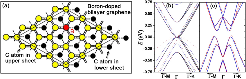
Figure 18. Boron-doped bilayer graphene and their band structures. (a) Representative 3 × 3 supercells, the red atom denotes a substitutional boron atom. (b) Band structure for pure bilayer graphene (black full line) and for two short-range models for boron impurities in a 3 × 3 cell, using an on-site potential of 4.2 eV at the impurity site and nearest-neighbor hopping energies of −1.68 eV (red dotted line) and −3.12 eV (blue dashed line) between boron and carbon. (c) DFT (blue full line) and tight-binding (red dashed line) band structures of substitutional boron-doped bilayer graphene in a 3 × 3 supercell. Reprinted with permission from [201]. Copyright 2010 by the American Physical Society.
Download figure:
Standard imageIn addition to nitrogen and boron doping, substitutional doping of graphene with other heteroatoms, such as sulfur [206–208], phosphorus [208, 209] and silicon [210], has also been investigated theoretically. Using first-principles calculations, it was found that sulfur doping could induce different effects: the doped sheet can be a small-band-gap semiconductor, or it could exhibit enhanced metallic properties when compared with a PG sheet [206]. Therefore, S-doped graphene (SG) may also be a smart choice for constructing nanoelectronic devices, since it is possible to vary the electronic properties of the sheet by adjusting the doping level of sulfur into the graphene lattice. Moreover, DFT investigations show that the DOS of SG at the Fermi level actually increases upon NO2 adsorption, as is visible in figure 19, which demonstrates that S-doped graphene could be used as an efficient sensor for some toxic gases due to the high selectivity of this material [207]. Regarding phosphorus-doped graphene (PhG), our previous work has found out that phosphorus will maintain an sp3 hybridization, and bonds to the carbon atoms with tetrahedral orbitals, inducing structural strain in the carbon lattice (figure 20(a)) [211]. Using first-principles periodic calculations, Denis demonstrated that the doping of P atoms into the graphene lattice could open the largest band gap (0.67 eV spin up, 0.66 eV spin down, figure 20(b)) compared with the cases of Si-, Al- or S-doped monolayer graphene [212]. If gases, such as NO2, NO, SO2, are adsorbed onto PhG, the electronic conductivity of the PhG will be changed [209]. By monitoring the conductivity variation after the adsorption of molecules, the PhG can also be used as a sensitive detector of these toxic gases.
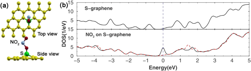
Figure 19. Sulfur-doped graphene (SG) and its potential for detecting NO2 gas molecules. (a) The most stable configuration of SG with adsorbed NO2. (b) The DOS for NO2 on SG. The solid line is the DOS of the majority spin and the dashed red line is the minority spin. The vertical dashed line represents the Fermi level of the system, which is set to zero here. The upper figure is the DOS versus energy of SG without NO2. Reprinted with permission from [207]. Copyright 2009 by the American Institute of Physics.
Download figure:
Standard image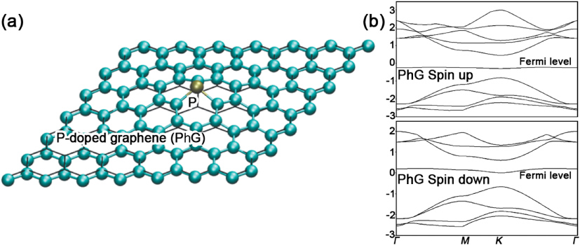
Figure 20. Phosphorus-doped graphene (PhG) and the adsorption of different molecules. (a) Relaxed structure of PhG. Reprinted with permission from [211]. Copyright 2009 by the American Chemical Society (b) Band structure of 4 × 4 phosphorus-doped monolayer graphene. Reprinted with permission from [212]. Copyright 2010 by Elsevier Ltd.
Download figure:
Standard imageFor Si-doped graphene, theoretical calculations have demonstrated that it is more favorable to use bilayer graphene in order to reduce the formation energies. In this sense, a bond between the two Si atoms in each layer will be formed without significantly altering the stacking interaction (figure 21(a)). The formation of such bonds in bilayer graphene could reduce the formation energy compared with that of monolayer graphene [213]. Based on these calculations, Si-doped graphene (SiG) will have potential applications in areas such as toxic gas sensing [210] and organic compound detection [214]. For example, melamine (C3H6N6) is a deleterious compound for human health, which may appear in our food nowadays and should be detected by suitable sensors. Using first-principle calculations, Wang et al demonstrated that the melamine-SiG (figure 21(b)) has the most stable configuration when compared with P-, B- or N-doped graphene. The band structure of SiG will change remarkably before and after the melamine adsorption due to charge transfer (figure 21(c)) [214]. However, more experimental efforts are also urgently needed in research related to SiG.
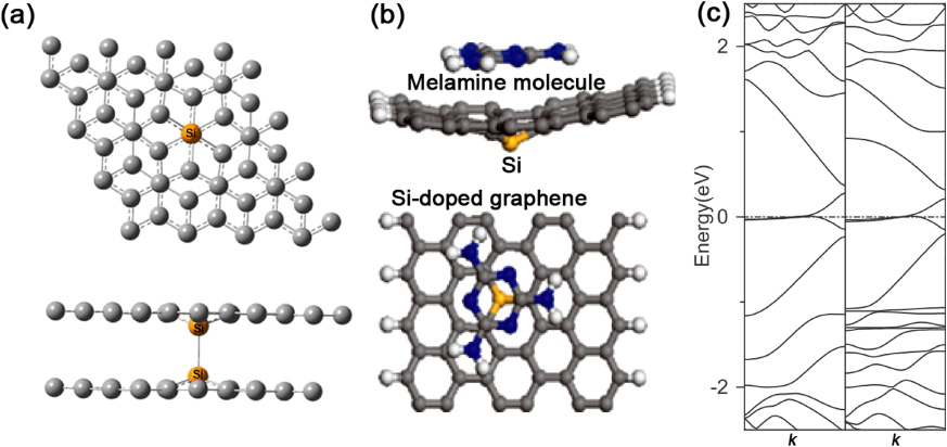
Figure 21. Silicon-doped graphene (SiG) and the interaction with a melamine molecule. (a) Optimized structure for bilayer graphene doped with Si in vacancy sites. Reprinted with permission from [213]. Copyright 2011 by Elsevier Ltd. (b) GNRs with Si-dopant in vacancy sites interacting with melamine. (c) Band structures of the Si-doped GNRs before (left panel) and after (right panel) adsorbing the melamine molecule. The Fermi level is indicated by the horizontal dotted line. The wave vector k is plotted from Γ to X in both cases. Reprinted with permission from [214]. Copyright 2010 by Elsevier Ltd.
Download figure:
Standard image5.1.2. Reduced graphene oxide
In order to tune the electronic properties of graphene, the controlled reduction of GO appears to be an efficient route to modulate the band gap. GO shows a gap greater than 0.5 eV at room temperature, and GO could exhibit semiconducting behavior when it is reduced into graphene [182], because some residual oxygen and structural defects remain within the structure of reduced GO, as shown in figures 22(a) and (b) [215, 216]. A detailed discussion, focused on the synthesis, properties and applications of GO, can be found in various reviews available in the literature [176, 217–219].
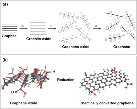
Figure 22. Chemically converted graphene by the reduction of GO. (a) The chemical route to the synthesis of solubilized graphene. Reprinted with permission from [216]. Copyright 2008 by Nature Publishing Group. (b) 3D molecular models of graphene oxide and chemically converted graphene demonstrate that the removal of the–OH and–COOH functionalities upon reduction restores a planar structure. Reprinted with permission from [215]. Copyright 2009 by Nature Publishing Group.
Download figure:
Standard image5.2. Importance of the dopant site and property changes
As mentioned above, the chemical doping of graphene and GNRs could be considered as an efficient route able to tune the electronic and quantum transport properties of graphene-like materials. In addition to the chemical nature of the dopant, the location of the doping atoms in the structure and the dopant concentration are very important factors that control the physicochemical properties of doped graphenes. DFT calculations on GNRs have demonstrated that edge functionalization of armchair ribbons does not show remarkable band gap changes against N or B edge substitutions. However, N, B and pyridine-like bulk substitutions could cause semiconductor–metal transitions, as shown in figure 23(a) [186]. Moreover, the concentration of vacancy or dopant defects also affects the electrical properties of graphene. Figure 23(b) shows the variation of the electrical conductivity as a function of different vacancy or nitrogen doping concentrations in graphene. It demonstrates that a minimum resistivity could be found for around 0.5% vacancy or nitrogen dopants. However, the resistivity in the metallic regime (concentration > 0.5%) is lower for nitrogen doping when compared with a vacancy, which could partially be attributed to the N atoms, responsible for providing electron carriers to the material, shifting the Fermi level much more than for the case of vacancy defects [220].
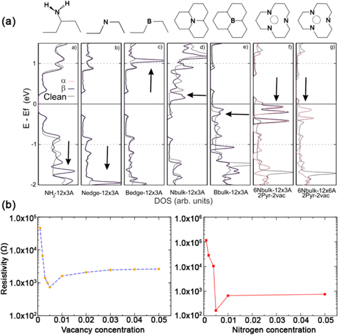
Figure 23. The doping sites and the effect of doping and vacancy concentrations on the electrical properties of graphene. (a) Spin density of states of functionalized AGNRs doped with nitrogen (N) and boron (B) atoms in various configurations as shown above each DOS plot. Reprinted with permission from [186]. Copyright 2008 by the American Physical Society. (b) Calculated resistivity of monolayer graphene as a function of vacancy (left) or nitrogen (right) concentration. Reprinted with permission from [220]. Copyright 2010 by the American Physical Society.
Download figure:
Standard imageThe Terrones group has carried out structural relaxation and transport calculations on doped armchair nanoribbons using the DFT method [221]. The nanoribbons were substitutionally doped by replacing one carbon atom by B, N, O, Si, P or S atoms, and the edges were passivated with hydrogen. It can be observed from figure 24(a) that the optimized structures when doping with N (or B) are slightly modified but preserve the honeycomb lattice. Only the bond lengths surrounding the dopants are slightly altered. However, for S- and P-doped nanoribbons, the structures are significantly modified; that is, the dopant in these cases prefers to 'pop out' of the plane, and the carbon and hydrogen atoms located near the edges also remain out of the plane, as shown in figure 24(a). The quantum transport properties of chemically doped AGNRs are shown in figure 24(b). The quantum conductance plots reveal similar features at and around the Fermi level, and the doped nanoribbons exhibit semiconductor behaviors. For low doping levels (one doping site per ∼100 atoms), a linear I–V response could be observed for B-, N-, Si- and P-doped nanoribbons (figure 24(c)). However, for O- and P-doped ribbons, a higher applied voltage is needed to reach the same current values as are observed for the above-mentioned doping cases. Based on these calculations, it can be predicted that GNRs doped with Si could be used in interconnector electrical devices, whereas nanoribbons doped with P could be used for the fabrication of sensors.
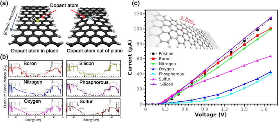
Figure 24. GNRs doped with different atoms. (a) Relaxed structures of substitutional doping in AGNRs. (b) Quantum conductance versus energy for doped AGNRs compared with the pristine ones (see the dotted lines) for zero applied voltage. In all cases, the ribbons retain the semiconductor feature in the conductance in the vicinity of the Fermi level; however, the detailed conductance curves depend sensitively on the dopant atom. (c) Electronic current as a function of the applied voltage for doped and pristine AGNRs. Reprinted with permission from [221].
Download figure:
Standard image5.3. Functionalization
In addition to the above-mentioned substitutional dopants into the graphene lattice, there are some other chemical routes to functionalize graphene, such as hydrogen passivation [153, 222], molecule grafting [223–225] or modification with different functional groups [154, 226]. Novoselov and co-workers have demonstrated that atomic hydrogen could react with graphene and transform this highly conductive zero-gap material into an insulator [222]. The as-obtained graphene derivative, so-called graphane, is crystalline and retains the hexagonal lattice, but its in-plane periodicity becomes remarkably shorter than that of graphene, due to the atomic-scale buckling caused by the hybridization change from sp2 to sp3 bonding. In addition, based on the configuration of a graphite intercalation compound (GIC), by inserting some ions or molecules, such as diazonium cations (figure 25(a)) [224] or hydrophobin (figure 25(b)) [225], into the interlayer spacings of graphite and then exfoliating the resulting intercalation compound, a kind of surface-functionalized graphene could be obtained. This covalent functionalization could protect the single-layer graphene from re-aggregation. Furthermore, the attachable functional groups might also provide graphene with some tailor-made properties, such as customizable solubility, electron mobility and sensor activity. Using GGA for the density functional, Boukhvalov et al have considered the functionalization of bilayer graphene by different functional groups [226], namely, OH, CN, NH2, CH3, COOH as well as by combination of the dopants and hydrogen, as shown in figure 25(c). It has been demonstrated by their calculations that the gap of graphene can be tuned smoothly between 2 and 3 eV with an accuracy of about 0.2 eV [226]. Therefore, chemical functionalization will also be an efficient route for developing high-performance applications of graphene- and graphane-based materials in the area of molecular electronics, and further work along this research line is still needed.
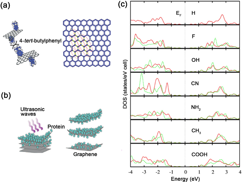
Figure 25. The functionalization of graphene. (a) Representation of the 4-tert-butylphenyl functionalized graphene and transpolyacetylene (t-PA) chains formed by the introduced sp3 sites (hydrogen atoms are used in this example) in the sp2 carbon layer (highlighted in yellow). Reprinted with permission from [224]. Copyright 2011 by Nature Publishing Group. (b) Hydrophobin-functionalized graphene obtained by ultrasonic waves. Reprinted with permission from [225]. Copyright 2010 by Wiley-VCH Verlag GmbH & Co. KGaA, Weinheim. (c) Total densities of states versus energy for one-side (solid red lines) and two-side (dashed green lines) functionalizations of bilayer graphene for the case of hydrogen (H), hydroxyl (OH) and other species. Insets show optimized atomic configurations for the case of two-side functionalization. Reprinted with permission from [226]. Copyright 2008 by the American Physical Society.
Download figure:
Standard image6. Applications
In this section, some of the important applications of graphene and GNRs will be demonstrated and summarized. We believe that the applications listed below, such as in high-performance FETs, sensor devices, energy storage devices, transparent electrodes, only constitute the tip of the iceberg and more and more fascinating applications will be developed in the near future based on these interesting 2D and 1D carbon nanostructures with unique physical properties.
6.1. Graphene-based field-effect transistors
Due to their attractive properties, such as high electron mobility, electron-hole symmetry, quantum Hall effect [28, 227] and strong suppression of weak localization effects [228, 229], graphene has great potential in high-speed and high-frequency electronics applications. A top-gated graphene FET operating at high frequencies (gigahertz) was developed in 2009 by IBM researchers [230], and soon after that, transistors operating at 100 GHz [231] and 300 GHz [232] were reported in 2010. In June 2011, IBM researchers [233] reported their work on a wafer-scale integrated circuit (IC) using graphene field-effect transistors (G-FETs) (figure 26). Graphene circuits were fabricated on a semi-insulating SiC wafer. A two- or three-layer graphene film was epitaxially grown on the Si face of the SiC substrate at temperatures above 1400 °C. Fabrication of the graphene IC began with top-gated, two-finger G-FETs (figure 26(a)), followed by integration with on-chip inductors. In order to form the active channel of the transistor, these authors spin-coated the graphene-SiC wafer with a layer of 140 nm thick PMMA (poly(methyl methacrylate)) followed by a layer of 20 nm thick HSQ (hydrogen silsesquioxane). The FET channel was defined by e-beam lithography (EBL); the surrounding graphene was removed by oxygen plasma with the exposed HSQ film as the protecting mask. The optical image of a completed graphene mixer and its schematic illustration are shown in figures 26(b) and (c), respectively. Figure 26(d) displays the output frequency spectrum of the graphene mixer with input signals fRF = 3.8 GHz and fLO = 4 GHz and a drain bias of 2 V. This work [233] demonstrates that a graphene IC can operate as a broadband RF mixer at frequencies up to 10 GHz with excellent thermal stability. The excellent transistor performance achieved in such graphene-field-effect transistor (G-FET) devices should open exciting opportunities in high-speed, high-frequency electronics.
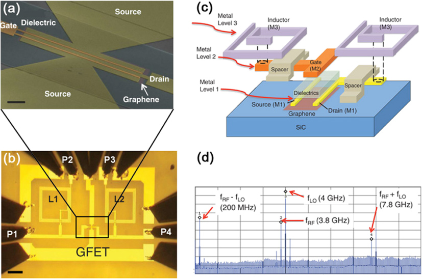
Figure 26. A wafer-scale graphene integrated circuit (IC). (a) Scanning electron image of a top-gated, dual-channel graphene transistor used in the mixer IC. The gate length is 550 nm and the total channel width (including both channels) is 30 µm. Scale bar: 2 µm. (b) Optical image of a completed graphene mixer including contact pads. Scale bar: 100 µm. (c) Schematic exploded (zoom) illustration of this graphene mixer circuit. (d) A snapshot of an output spectrum, between 0 and 10 GHz, of the mixer taken from the spectrum analyzer with two high-frequency input signals, an RF signal at a frequency of fRF = 3.8 GHz and a local oscillator (LO) signal at a frequency of fLO = 4 GHz. Reprinted with permission from [233]. Copyright 2011 by the American Association for the Advancement of Science.
Download figure:
Standard image6.2. Transparent conductive electrodes
Optoelectronic devices, such as touch screens, light-emitting diodes and solar cells require materials with low sheet resistance and high optical transparency. As a 2D single atomic layer of crystalline carbon, graphene exhibits high room-temperature carrier mobility [234], a tunable band gap [197], ballistic transport [235] and a visible transparency of 97.7% [236, 237]. Hence, ideal materials for applications in electronics and optoelectronics, include their use in transistors, photodetectors and saturable absorbers of light [238]. Graphene thin films exhibit a high optical transparency in both the visible and near-infrared regions of the spectrum, a low electrical resistivity, high chemical and thermal stabilities, high carrier mobilities. These properties make graphene an excellent choice for transparent electrodes in various optoelectronic devices [239]. For instance, a liquid crystal display (LCD) made using a sheet of peeled graphene as the transparent conductor has been demonstrated [240]. It was found that each layer of graphene absorbs about 2.3% of the incident light, which is significantly lower than that of conventional indium tin oxide (ITO) (15–18%) [241]. Furthermore, graphene has shown great potential for creating photovoltaic solar devices owing to its high optical transmittance and electrical conductivity. The graphene film not only serves as a transparent electrode for light transmission but also as an active layer for electron/hole separation and hole transport [242, 243]. Graphene microsheets have been dispersed into conjugated polymers to improve the polymer exciton dissociation and charge transport [244, 245]. Solution-processed thin films were used as conductive and transparent electrodes for organic [246] and dye-sensitized [239] solar cells, although the cell efficiency is still lower than those with ITO and fluorine tin oxide (FTO) electrodes [239], and further work is needed to realize the full potential of graphene for these applications. The application of graphene in inorganic thin-film solar cells has also been explored. Li et al demonstrated an efficient solar cell by forming Schottky junctions between graphene sheets and Si [247]. This sheet consisted of multiple layers of graphene that are overlapped and interconnected, which ensures a conducting pathway even if there are cracks formed in one of the graphene layers. The multilayer structure is expected to provide a higher carrier mobility based on a recent study on graphene layers decoupled from bulk graphite [248]. Moreover, graphene thin films also exhibit great mechanical properties and can be used to make flexible and stretchable electrodes [249, 250]. However, in order to produce graphene-based transparent conductive film, there is still a long way to go. For example, graphene films should exhibit optical transparency of 90% (λ = 550 nm) as well as a sheet resistance below 80 Ω/sq, and they should be sustainable after bending without degradation of performance.
6.3. Graphene-based sensors
The properties of graphene in biosensors and gas sensing have been widely investigated. For example, using reduced graphene oxide to construct a 3D structure of graphene-encapsulated SiO2 nanoparticles, the detection limit for target cancer biomarkers has been remarkably improved [251]. Wang et al have demonstrated that N-doped graphene can be used for glucose biosensing with concentrations as low as 0.01mM in the presence of interferences including ascorbic acid (AA) and uric acid (UA) for testing the selectivity [252]. Schedin et al showed that mechanically exfoliated graphene flakes can detect a single molecule of NO2 gas [253]. They fabricated micrometer-size sensors made from graphene, and such a device was capable of detecting an individual gas molecule when it interacts with the graphene surface. Each adsorbed molecule changes the local carrier concentration in graphene by one electron, which leads to step-like changes in the resistance. The high sensitivity that is achieved is due to the fact that graphene is an exceptionally low-noise material electronically, which makes it a promising candidate not only for chemical detectors but also for other applications where local probes sensitive to external charge, magnetic field or mechanical strain are required. Graphene-based gas sensors allow the ultimate molecular sensitivity since the adsorption of individual gas molecules can now be detected. Large arrays of such sensors would increase the uptake area [254], allowing higher sensitivity for short-time exposures and the detection of active (toxic) gases in as low a concentration as would be practically desirable. Chemically modified graphene has been used in biosensor applications. For example, immunoglobulin E aptamers with an approximate height of 3 nm were successfully immobilized on a graphene surface. The aptamer-modified G-FET showed selective electrical detection of IgE protein, exhibiting good affinity and the potential for G-FETs to be used in biological sensors [255]. Hou et al found that graphene modified with ethylenediamine triacetic acid (EDTA) can be used as an ideal electrode material to fabricate biosensors [256]. They fabricated a dopamine electrochemical biosensor with a high selectivity and sensitivity, which might allow its potential use in the investigation and diagnosis of dopamine-related diseases.
6.4. Energy storage and conversion
Pristine and doped graphene has been demonstrated as an electrode material for capacitors [257, 258] and lithium ion batteries [259, 260], because of both its high specific surface area (2630 m2 g−1) and unique 2D structure. The discharge capacity of graphene in a lithium ion battery was found to be 540 mAh g−1, and this could be further improved to 730 and 784 mAh g−1 by adding CNTs and fullerenes to the graphene [261]. Graphene also showed a good ability to coat silicone particles, and metal or metal oxide particles in order to prevent the volume expansion of the electrode materials during the charge and discharge cycles in batteries [261–263]. The supercapacitor is recognized as one of the important next-generation rechargeable power sources due to its intrinsic ability to decrease the gap between the dielectric capacitor and the battery. In addition, the edge site is known to have a differential capacitance ten times higher than that of the basal plane [264]. Thus, graphene could be used as an electrode material for supercapacitors. Miller et al have demonstrated high-performance electric double-layer capacitors (DLCs) with electrodes made from vertically oriented graphene nanosheets grown directly on metal current collectors. This design minimized electronic and ionic resistances and produced capacitors with a resistor–capacitor (RC) time constant of less than 200 ms, which is much faster than that of typical DLCs (∼1 s). This fast time constant can be attributed to these aligned graphene nanosheets showing more exposed edge planes that greatly increase the charge storage as compared with that of designs that rely on basal plane surfaces only. Moreover, in order to improve the performance of these graphene-based supercapacitors, several approaches have been developed, such as controlling the surface area and edge sites [265], and by introducing metal oxide [266]. In addition to this, graphene can also be used in the fuel cell area by virtue of its excellent ability to support metal nanoparticles (Au, Pt and Pd) [267–270]. We believe that more and more interesting electrochemical properties of graphene will be explored for their applications in energy storage and conversion in the future.
6.5. Other applications
In addition to the above-mentioned applications, graphene could also be used in areas such as SERS [271], hydrogen storage [272], field-emission [273] or for catalyst supports [274]. Mülhaupt and co-workers demonstrated that palladium nanoparticles dispersed on graphite oxide were able to catalyze Suzuki–Miyaura coupling reactions [274]. (The Suzuki–Miyaura reaction is a valuable synthetic process for the construction of carbon–carbon bonds). Seger et al used graphene as a support material for the dispersion of Pt nanoparticles for the development of a fuel cell electrocatalyst [275]. In addition, graphene–TiO2 nanocomposites can be employed as photo-anodes in a photo-electrochemical cell. In this context, the role of graphene is mainly to promote the collection and transport of photo-injected electrons [276]. Efforts are also being made to utilize graphene-based composites for visible-light-induced photo-electrolysis of water [276].
7. Conclusions and perspectives
In this review, we focused on defects in graphene as a model system for studying defects in 2D and 1D sp2 hybridized carbon systems. We demonstrated that point defects and line defects of various types produce different and significant changes in the physical, magnetic and chemical properties of graphene-like nanomaterials. We showed that defects introducing disorder could in general be detrimental to the proper functioning of various properties, but for other properties such as n-type or p-type doping, the introduction of dopants which also introduce structural defects could be used to further control the carrier concentration, so there is a trade-off between the materials benefit and the degradation that needs to be balanced and optimized. Some defects, such as edges, are of great interest for the new physics they introduce. For atomically smooth graphene edges, potential applications of the edges are contemplated, and the characterization of edge types has been important. HRTEM has been shown to provide a powerful technique for carrying out such studies, but Raman spectroscopy coupled with theory has also provided a surprisingly useful and convenient probe of graphene edges and graphene ribbons, even though the wavelength of light is orders of magnitude larger than graphene ribbon widths, or CNT diameters for that matter. Defects are symmetry breaking, and therefore allow vibrational modes that are normally Raman or IR inactive to become activated. This tool has not been sufficiently developed for the study of defects and should be considered as an attractive topic for future study. It might be that one could identify and distinguish between different defect types and quantify the density per unit area or per unit volume for the different defect types by carrying out a perfectly designed spectroscopy experiment. From a practical standpoint, the functionalization of graphene could be used to improve certain chemical properties of graphene, such as solubility and dispersability. But at the same time, functionalization introduces foreign atoms into the lattice or edges, and the associated processing conditions also are likely to introduce defects. Nevertheless, the benefits of functionalization often outweigh the degradation effects of the foreign atoms as discussed above in general terms. Thus, it is crucial to synthesize perfect or atomically smooth edges in GNRs to establish baselines for comparison, and it is crucial to control the location distribution and total amount of dopants in graphene and GNRs. In addition, it is important to emphasize that there are other defects we did not discuss in this review, such as screw dislocations and interlayer stacking faults, and this is because such defects are not important for a monolayer graphene 2D crystal, but could become quite important in few-layered graphene. Therefore, these types of defects should now be studied and theoretical calculations should be performed.
In a 2D crystal such as graphene, 1D and point defects produce significant changes in their physicochemical properties which should be considered in the future to perform defect engineering at the nanoscale. Such defects include edge geometry, vacancies, topological 5–7, D5D7, 5–8–5, T5T7, grain boundaries, extended lines of defects and doping, all of which might play a role in future applications. But also this knowledge can be extended to other layered materials, such as boron nitride and metal dichalcogenides (MoS2, WS2, MoSe2, etc) to broaden the spectrum of different behaviors and applications (figure 27), with each system providing nuances that could enrich developments among the different layered materials. Certainly, HRTEM, STM, STS, Raman and other spectroscopies, and synthesis methods to study defects need to be further developed and improved not only to characterize defects in graphitic nanostructures but also to produce specific defects, in an ordered way in different layered systems in order to create more reliable and useful functional materials.
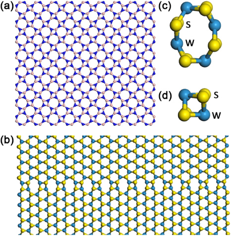
Figure 27. (a) BN-Haeckelite-8–4. (b) Extended line of defects in a WS2 sheet formed by octagonal-like defects and a square-like defects, as shown in (c) and (d), respectively.
Download figure:
Standard imageAlthough there are numerous challenges remaining for future study, we can now see that when we gain some control over the defect type, defect location and defect concentration, we will be able to produce novel materials with fascinating properties that could revolutionize energy-related applications and bio-nanotechnology.
Acknowledgments
We acknowledge the support from the Research Center for Exotic Nanocarbons, Japan regional Innovation Strategy Program by the Excellence, JST (MT). MSD is grateful for support from MURI-Navy ONR, Contract: N00014-09-1-1063 and HTM acknowledges funding from Programa Professor Visitante do Exterior-PVE as 'Bolsista CAPES/BRASIL'. MT thanks the Penn State Center for Nanoscale Science for a seed grant entitled 'Defect Engineering of 2-D Sheets of Layered Materials'.