

Abstract
The threshold voltage degradation due to the hot carrier induced localized charges (LC) is a major reliability concern for nanoscale Schottky barrier (SB) cylindrical gate all around (GAA) metal–oxide–semiconductor field-effect transistors (MOSFETs). The degradation physics of gate material engineered (GME)-SB-GAA MOSFETs due to LC is still unexplored. An explicit threshold voltage degradation model for GME-SB-GAA-MOSFETs with the incorporation of localized charges (Nit) is developed. To accurately model the threshold voltage the minimum channel carrier density has been taken into account. The model renders how +/− LC affects the device subthreshold performance. One-dimensional (1D) Poisson's and 2D Laplace equations have been solved for two different regions (fresh and damaged) with two different gate metal work-functions. LCs are considered at the drain side with low gate metal work-function as Nit is more vulnerable towards the drain. For the reduction of carrier mobility degradation, a lightly doped channel has been considered. The proposed model also includes the effect of barrier height lowering at the metal–semiconductor interface. The developed model results have been verified using numerical simulation data obtained by the ATLAS-3D device simulator and excellent agreement is observed between analytical and simulation results.
Export citation and abstract BibTeX RIS
1. Introduction
A Schottky barrier cylindrical gate all around (CGAA) metal–oxide–semiconductor field-effect transistor (MOSFET) with metal source/drain (S/D) instead of the usual highly doped S/D is an excellent candidate for low power, high speed and extremely scaled MOS devices in the nano regime [1]. It offers low S/D interface contact resistivity for metallic S/D compared with doped S/D [2]. It solves the major bottlenecks of device scaling such as a very shallow S/D junction, difficult doping techniques, and a thermal budget which makes it a futuristic alternative for next-generation MOS device [3, 4]. Furthermore, the lightly doped (Na ≤ 1016 cm−3) SB-CGAA device alleviates problems such as mobility degradation and random dopant fluctuation [5]. For the formation of the high-k dielectric, low-temperature processing is very important. Therefore, the SB-CGAA MOSFET is best suited as it requires low-temperature processing [6].
Long-term reliability of these nanoscale devices is also an important issue. However, undoped SB-CGAA MOSFET shows excellent immunity to short channel effects (SCEs) but the localized charges/interface trap charges at the Si–SiO2 interface causes the threshold voltage and subthreshold slope (SS) degradation [7, 8]. The increased density of integration of these nanoscale devices on integrated circuits raises the possibility of the generation of interface trap charges. These localized charges are created either during the manufacturing process (stress-induced damage, radiation-induced damage) or by hot carriers, under high applied drain voltage near the drain-channel junction, giving rise to localized charge pile up of interface traps (Nit) near the drain-channel region [9]. In particular, these generated localized trap charges due to high electric field (leading to hot carrier generation) results in threshold voltage shift, and SS degradation by surpassing the barrier at the Si–SiO2 interface and will disintegrate the original performance of the device and finally lead to permanent device failure [10, 11]. Previously the hot carrier degradation (HCD) mechanism based on Si–Si, Si–O and Si–H bond breaking has been thoroughly studied [12–14].
To understand the physics of SB-CGAA MOSFETs a few models have been reported [15, 16] but all of them neglected the impact of localized charges/interface charges. This work concentrates on developing the model for SB-CGAA MOSFETs to explore the effect of +/ interface trap charge (ITC, Nit) generated under hot carrier stress. Gate material engineering (GME) is a well-explored technique to mitigate the hot carrier effects (HCEs) which enhances the carrier transport efficiency by suppressing the effect of Nit [17–19]. In GME the work function of gate metal towards the drain side is lower than the gate metal work-function at the source side. A dual metal gate architecture is employed to reduce the electric field at the drain side to evaluate the effect of Nit on GME.
A two-dimensional (2D) threshold voltage model using the superposition technique has been developed. For the derivation of surface potential and Vth, 1D Poisson's and 2D Laplace equations have been solved. Finally, an analytical model is developed to model the behaviour of Nit with the incorporation of dual metal gate (DMG or GME) architecture. Developed model results are compared with the results obtained from the ATLAS-3D simulations and a close agreement is observed and is useful for designing low power, high-speed and high-frequency devices and charge trap memory devices. SB-CGAA MOSFET calibration and enhanced analog/RF performance of the DMG-SB-CGAA MOSFET over a single metal gate (SMG) SB-CGAA MOSFET has been shown in our previous work [20].
The developed model concentrates on the predictive subthreshold behaviour for a GME-SB-GAA MOSFET. For the developed model the device channel length and radius are restricted up to 40 nm and 10 nm, respectively. Quantum mechanical effects due to energy confinement are prominent in devices with channel length much shorter than 30 nm and radius of 5 nm regime [21–23], so in the present analysis, this aspect is neglected.
2. Device structure description
Figure 1 shows a 3D and cross-sectional view of the GME-SB-CGAA MOSFET. The structure has two different work-functions of the metal gate, M1 towards the source side with work-function ΦM1, and M2 towards the drain side with work-function ΦM2 with the gate lengths L0 and L1, respectively.
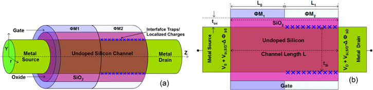
Figure 1. (a) 3D schematic of a SB-CGAA MOSFET, (b) cross-sectional view of the SB-CGAA MOSFET structure.
Download figure:
Standard image High-resolution imageThe silicon channel is lightly doped (NA = 1016 cm−3) with device channel length (L) 40 nm, radius R = 10 nm, gate oxide thickness tox = 3 nm, SiO2 permittivity εox = 3.9, gate metal work-function ΦM1 = 4.8 eV, ΦM2 = 4.4 eV, metal S/D work-function ΦS/D = 4.1 eV. The Shockley–Read–Hall (SRH) recombination model with concentration dependent lifetime is used to account for minority carrier recombination. The Boltzman transport model is used as a drift-diffusion model. The carrier-carrier scattering mobility model (CCSMOB), concentration dependent mobility model (CONMOB) along with Lombardi CVT (constant voltage and temperature) mobility model are used because they consider large temperature range with parallel and perpendicular field dependent mobility. The ATLAS-3D simulator has been used for numerical simulations [24]. Martin et al have shown the validity of the Atlas/Silvaco device simulator by comparing their Monte Carlo device simulation results with ALTAS-3D simulation results for Schottky barrier MOSFETs with excellent agreement [25].
3. Model derivation
3.1. Surface potential modeling
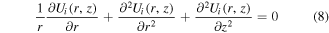
The silicon under the gate is assumed to be fully depleted. Channel potential including channel mobile carrier density is governed by Poisson's equation in two different regions and is given as
Here ψi(r, z) is the potential distribution in the silicon film, q is the electron charge, εSi is the permittivity of silicon, i = 1 and 2 shows the undamaged (region 1) and damaged (region 2) regions, respectively. NA is the doping of silicon film.
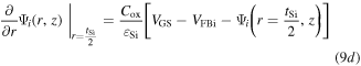
For nanowire devices, the oxidation process during fabrication is done at high temperature (∼900 °C) under a precise clean room environment. Consequently very fine oxide is grown [26] with the least number of interface trap charges (∼1 × 10¹⁵ m−2), which is negligible [27]. So the impact of interface trap charges at the source side will be negligible on drain current characteristics. At the drain side however, induced hot carriers will increase the interface charge concentration (∼1 to 5 × 10¹⁶ m−2) and it will no more be negligible [9–11, 28]. So we consider separate flat band voltage for two regions which are written as

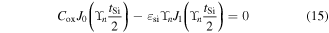
where Nit is the density of the localized charge/interface trap, ΦSi is the silicon work-function and Cox is the gate oxide capacitance per unit area of the GME-SB-CGAA MOSFET and is given as

and

where χ is the electron affinity of silicon, Eg is the energy band gap and ΦF is the Fermi potential. It can be noted that apart from different interface charge in the two regions, gate metal work-functions will also differ (ΦM1 in undamaged and ΦM2 in the damaged region) and this is taken into account in equations (2) and (3). By using the superposition technique, the solution of electrostatic potential ψi(r, z) can be decomposed into two components: the long channel solution Vi(r) and short channel solution Ui(r, z), where Vi(r) and Ui(r, z) are the solutions of the 1D Poisson equation and 2D Laplace equation, respectively. Then the electrostatic potential in a SB-CGAA MOSFET can be written as

Equation (1) is then decomposed into equations (7) and (8) as
where i = 1 for the undamaged region (with ΦM1) and i = 2 for the damaged region (with ΦM2). 1D potential Vi(r) can be obtained by solving Poisson's equation with the following boundary conditions:
- a.Potential at the centre of the silicon pillar is ψc,

- b.Electric flux at the centre of the silicon pillar is zero,
- c.Potential at the surface of the silicon pillar
- d.Electric flux at the surface of the silicon pillar is continuous


The solution of 1D Poisson equation (7) using the boundary conditions given in (9a)–(9d) can be expressed as
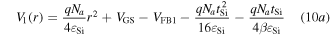
and
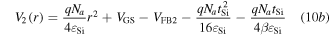
Here VGS is the gate-to-source voltage; tSi is the diameter of the silicon pillar and β = Cox/εSi. The solution of 2D Laplace equation (8) can be obtained using the following boundary conditions:
- a.At the interface of two different metal gates, potential is continuous
- b.At the interface of M1 and M2, electric field is continuous


- a.Potential at the source end
- b.Potential at the drain end


Here Vbi,S/D is the built-in potential at the S/D, ΔΦbS and ΔΦbD are SB lowering at the source and drain, respectively [29, 30] and can be expressed as

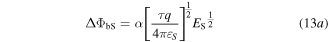
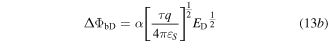
Here χ is the electron affinity of silicon, εSi is the silicon permittivity, ES and ED are the electric fields at the source and drain end, respectively. α and τ are treated as fitting parameters (α = 1, τ = 1.1) [24].
The solution of equation (8) using the above boundary conditions can be expressed as
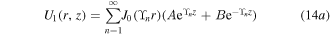
and
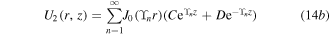
A, B, C and D are the Bessel–Fourier series coefficients and are given in
J0 and J1 are the Bessel function of order zero and one, respectively.
3.2. Threshold voltage
For DMG architecture, the position of minimum surface potential resides under the metal gate with the higher work-function. The position of minimum surface potential is obtained by equating the derivative of Ψ1 (z) to zero and is obtained as
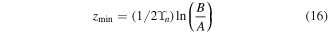
Thus the value of minimum surface potential is obtained as
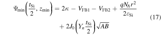
where A, B and  are given in the
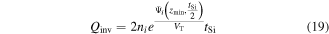
Qinv is obtained by taking integration of their spatial density for the entire thickness of the channel and can be expressed as

The value of the integral in equation (18) can be approximated by taking its value at r = tSi/2 as
On solving equation (19) with case (i) Qinv → Qth, and (ii) VGS → Vth, an expression of threshold voltage can be obtained as
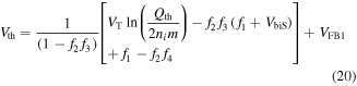
where f1, f2, f3 and f4, are given in the
3.3. Subthreshold slope
SS given by equation (21) is an important parameter of the subthreshold region of operation for the MOSFET, and it is generally defined as the shift in the applied gate bias i.e. VGS required to reduce the subthreshold current by one decade. For a GME-SB-CGAA MOSFET to have an excellent turn-on characteristic, SS should be as low as possible [34]. The minimum attainable SS value for any device at room temperature is nearly 60 mV/dec. But due to the presence of interface trap density, the surface state capacitance modifies the VFB and SS changes and increases or decreases depending upon the type of interface trap charge (ITC) (+/−). Hence it is a suitable parameter to measure the impact of the interface traps on device performance, written as
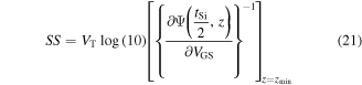
where zmin can be calculated from (16). Equation (21) shows the direct dependence of SS on zmin which is affected by Nit. So it also reflects the degradation of SS due to interface traps generated by hot carrier degradation which increases as time passes. The increase in SS slows down the device switching performance.
3.4. Subthreshold current
The total subthreshold current is due to the thermionic current and the tunneling current, given as
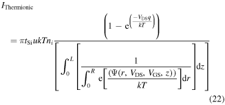
and
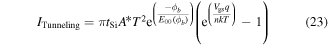
Here μ (0.13 m2 V−1 s−1) is the mobility, ni (1.45 × 1010 cm−3) is the intrinsic carrier concentration, A* is the Richardson constant, ϕb is the barrier height, and E00 is the constant of the material associated with the WKB expression and can be given as [35, 36]:


Here m*(0.26m0) is the effective mass of the electron, and m0 is the rest mass of the electron, k is the Boltzman constant,  where h is the plank constant. F and U are fitting parameters with values 21.8 and 36.6 (1/eV) [23], respectively.
The total subthreshold current is the combination of both Ithermionic and ITunneling [37] and is given as:

The other unknown symbols used above are given in the
4. Result discussion
Figure 2 shows the numerical simulation of drain current variation (in the log and linear scale) with respect to gate voltage for the device including quantum effects using the Bohr quantum model (BQM) and excluding quantum effects. It can be inferred from the figure that for a device size of R = 10 nm and L = 40 nm simulated drain currents are similar with and without BQM consideration. Hence in the present analysis quantum effects have been neglected. Thus its effect on the threshold voltage can also be neglected.
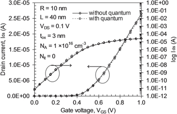
Figure 2. Variation of drain current as a function of gate voltage at normal and log scale, with/without quantum effect for a GMG-SB CGAA MOSFET.
Download figure:
Standard image High-resolution imageFlat band voltage (VFB) is an important and decisive parameter for a MOSFET device while calculating threshold voltage. The presence of localized ITC in the damaged region (towards the drain) caused additional band bending, thus altering VFB of the device [33]. Consequently, this results in threshold voltage degradation, which is a major reliability concern for low power memory devices.
Figure 3(a) shows the variation of valance band and conduction band energy profile with position along the channel at different Nit (+ve/−ve) ITC. This effect of the change in band bending due to ITC in VFB is incorporated using equation (3). It depicts that due to the presence of ITC in the damaged region the valance and conduction band energy is raised/lowered for negative/positive localized charges. The amount of change in VFB under the damaged region mainly relies on the oxide capacitance and the density of ITC. Figure 3(b) illustrates the variation of surface potential with position along the channel at different localized +ve/−ve ITC values. At the Si–SiO2 interface acceptor type traps accept an electron and the damaged region acts as a negative localized charge and the donor type interface traps act as a positive localize charge [38]. The effect of Nit generated by hot carriers depends on the instantaneous bias conditions. Since ITCs are electrically linked with the underlying Si, occupation of the traps depends on the Fermi level (EF) at the silicon and SiO2 interface and the interface states can be respectively positively charged (donor-type), neutral, or negatively charged (acceptor-type). In particular, interface state energy level (Eit) in the band gap with respect to the Fermi level decides the type of ITC: positive (Eit > EF) for donor-type and negative (Eit < EF) for acceptor-type interface states [39–41].
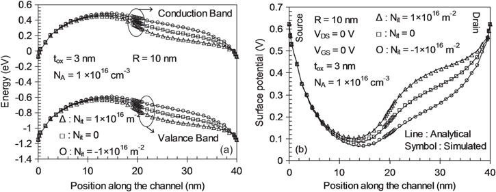
Figure 3. (a) Variation of valance and conduction band energy as a function of position along the channel for a GME-SB-CGAA MOSFET, (b) variation of surface potential as a function of position along the channel for a GME-SB-CGAA MOSFET for positive, negative and no ITC.
Download figure:
Standard image High-resolution imageHence due to negative localized charge the surface potential reduces and for positive localized charge the surface potential increases. GME devices are more immune to ITC compared to SMG MOSFETs as the variation of surface potential due to localized charges is more prominent in SMG MOSFETs [17, 18]. This is because of the low electric field with smaller metal gate work-function at the drain side in GME architecture. With the reduction of peak electric field in the channel, the carrier transport efficiency increases thus increasing the lifetime of the device.
It can be seen from the figure that even though the trap charges have been considered after the L/2 channel length and the minimum of the surface potential lies under the high metal gate work-function, the shift in potential is still clearly noticeable. This shift in potential (increase/decrease) is due to the change in flat band voltage.
Marchack et al [41] showed that the hot carrier induced localized charges are mainly prominent towards the drain side. So in the present analysis, the traps have been considered towards the drain side only and the ITC generated by radiation and stress induced damage (uniform in nature) are neglected. The effect of increasing positive trap charge density on surface potential has been shown in figure 4(a). In the case of donor type Nit, the surface potential in the damaged region rises under the lower metal gate work-function.
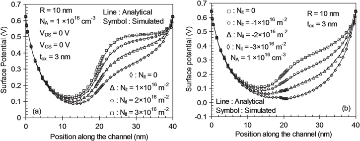
Figure 4. Variation of surface potential as a function of position along the channel for a GME-SB-CGAA MOSFET (a) with positive interface trap charges, (b) with negative interface trap charges.
Download figure:
Standard image High-resolution imageWith the increase in the density of positive trap charges the potential further rises and results in a shift of minimum surface potential in the channel in an upward direction. Change in minimum surface potential alters the normal threshold voltage (Vth) of a GME-SB-CGAA-MOSFET. The upward shift of the minimum surface potential results in a decrease of threshold voltage. The effect of increasing negative ITC on surface potential is shown in figure 4(b) and the lowering of the surface potential is more apparent for negative ITC. The lowering in minimum surface potential with the increase of negative ITC causes a increase of threshold voltage of the device. In the case of negative ITC, the drastic change in minimum surface potential is noticeable compared to positive ITC. In the case of Schottky barrier MOSFETs dangling bond or interface states at the metal–semiconductor interface causes an image force inside the channel and this process is called Fermi level pinning. The barrier height lowering due to this image force (defined in equation (13b)) is directly proportional to the charge under the screen gate region (region 2). And due to the nature of these interface states more lowering of surface potential in the case of negative ITC takes place. Furthermore, the device is a dual metal gate structure which has an abrupt junction at 20 nm length and there is an abrupt shift in surface potential as shown in figure 4(b). Due to the presence of localized charges in the damaged region (L ≥ 20 nm), the surface potential will shift in the downward direction. The surface potential shift directly depends on interface trap charge density and thus for higher trap charges it will shift further downward which affects the gradient of the surface potential profile at around 20 nm. The developed model shows an exact match with TCAD simulation. Figure 5(a) shows the variation of the threshold voltage for different values of –/+ ITC at different thicknesses of the gate dielectric (tox = 2, 3 nm). Based on the surface potential analysis of the positive/negative ITC the threshold voltage has been calculated (analytical) and is in good agreement with the simulated data.
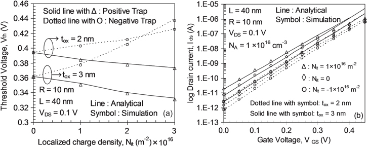
Figure 5. (a) Variation of threshold voltage as a function of interface traps density for a GME-SB-CGAA MOSFET, (b) variation of subthreshold current as a function of applied gate voltage for a GME-SB-CGAA MOSFET.
Download figure:
Standard image High-resolution imageThe change in Vth in the case of negative ITC is noticeable, whereas in the case of positive ITC for 3 nm gate dielectric thickness, Vth is less influenced by the donor type traps. Furthermore, for thinner gate oxide (tox = 2 nm) Vth of a GME-SB-CGAA MOSFET increases without any interface trap. This is due to the enhanced electrostatic control of the gate over the channel and the density of mobile carriers is susceptible to the gate oxide thickness at any applied VGS (gate voltage). The low oxide thickness (2 nm) has a similar impact of ITC on Vth for negative or positive ITC due to the improved control of the gate. The change in threshold voltage at different tox for different –/+ ITC values is tabulated in table 1 and it renders that the impact of positive Nit is almost similar to drain induced barrier lowering (DIBL) on Vth and SS, whereas the negative Nit counters the DIBL effect.
Table 1. Threshold voltage change due to −/+ ITC (m−2) at different gate oxide (tox) thicknesses.
| Threshold voltage, Vth (V) | |||||||
|---|---|---|---|---|---|---|---|
| 1 × 10¹⁶ m−2 | 2 × 10¹⁶ m−2 | 3 × 10¹⁶ m−2 | |||||
| tox | Nit = 0 | +ve | −ve | +ve | −ve | +ve | −ve |
| 2 nm | 0.394 | 0.384 | 0.403 | 0.378 | 0.4111 | 0.373 | 0.425 |
| 3 nm | 0.36 | 0.3515 | 0.377 | 0.339 | 0.405 | 0.33 | 0.437 |
The subthreshold behaviour of the device has great importance as it gives the amount of leakage in the device while turning the device on. Figure 5(b) shows the variation of subthreshold current of a GME-SB-CGAA MOSFET for different –/+ interface trap values. The presence of ITC changes the charge distribution in the channel and thus the flat band voltage in the damaged region changes. This leads to a change in surface potential and the threshold voltage of the device. It also degrades the subthreshold current and SS of the device. From the figure, it is clear that the negative ITC decreases the off-state current (Ioff) whereas positive ITC increases the off-state current (Ioff). The GME-SB-CGAA MOSFET is a lightly doped device and hence it offers reduced carrier mobility degradation. Therefore no substantial change in the on-current of the device takes place.
However, the increase (decrease) in Ioff due to positive (negative) ITC will definitely change the Ion/Ioff ratio of the device and will affect the original switching performance of the device while using digital applications and thus is a major reliability issue. Figure 6(a) shows the variation of the threshold voltage at different channel length for –/+ ITC. For the ITC values of 1 × 10¹⁶ m−2 and 3 × 10¹⁶ m−2, negative (positive) ITC causes an increase (decrease) in threshold voltage of the device. It is clear from the figure 6(a) that negative ITC shows more influence on Vth rather than the positive ITC. As is evident from figures 4(a) and (b) the negative ITC changes the position of the minimum surface potential more effectively compared to positive ITC, thus the shift in threshold voltage is also more prominent in the case of negative ITC. Figure 6(a) shows that for a long channel device (L = 80 nm) GME-SB-CGAA MOSFET, the ITC (either positive or negative) has a minor impact on threshold voltage shift. Figure 6(b) depicts the Vth variation at different channel radius of a GME-SB-CGAA MOSFET for different (−/+) ITC. It shows that with the variation of channel radius, positive ITC leads to a minor change in Vth but for negative ITC the change in Vth is noticeable.
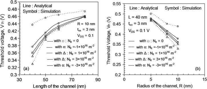
Figure 6. (a) Variation of Vth at different channel lengths, (b) variation of Vth at different radii of the silicon pillar, for a GME-SB-CGAA MOSFET at different −/+ ITC values.
Download figure:
Standard image High-resolution imageFigure 7(a) shows the variation of SS without the interface trap charges for tox = 2 nm and 3 nm. As the device channel length increases the SS value reaches closer to the theoretical limit of SS. The SS of a GME-SB-CGAA MOSFET for tox = 2 nm is lower than for tox = 3 nm, because of increased control of the gate over the channel which offers reduced Ioff. Figure 7(b) shows the SS at different channel lengths for positive ITC. As the channel length decreases the value of SS for positive ITC increases compared to the undamaged device. Figure 7(c) demonstrates the lowering of SS for the negative ITC.
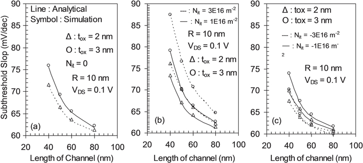
Figure 7. Variation of SS as a function of channel length for an SB-CGAA MOSFET for (a) no interface traps, (b) positive interface trap, and (c) negative interface trap.
Download figure:
Standard image High-resolution image5. Conclusion
In summary, Vth, SS and the subthreshold current degradation due to the different −/+ ITC in a GME-SB-CGAA MOSFET have been extensively studied by varying the device structural parameters such as channel length, channel radius and gate dielectric thickness. An extensive physics based localized/ITC dependent subthreshold current analytical model including Schottky barrier lowering has been developed for a GME-SB-CGAA MOSFET. The analytical results are in good agreement with simulation results and it can be concluded from the overall analysis that the −/+ localized charges cause increases (decreases) in surface potential, SS and subthreshold current. However, the result shows that the device is more immune to donor type traps and the effect of traps is reduced at low values of gate dielectric.
Acknowledgments
The authors are thankful to DRDO, Ministry of Defence, Government of India (ERIP/ER/1002196/M/1395) for providing the financial support to carry out this work. One of the authors (Manoj Kumar) would like to thank UGC, Government of India for providing the necessary financial support to carry out this research work.
