
Abstract
This paper presents a comprehensive review of the reliability issues hampering capacitive RF MEMS switches in their development toward commercialization. Dielectric charging and its effects on device behavior are extensively addressed, as well as the application of different dielectric materials, improvements in the mechanical design and the use of advanced actuation waveforms. It is concluded that viable capacitive RF MEMS switches with a great chance of market acceptance preferably have no actuation voltage across a dielectric at all, contrary to the 'standard' geometry. This is substantiated by the reliability data of a number of dielectric-less MEMS switch designs. However, a dielectric can be used for the signal itself, resulting in a higher Con/Coff ratio than that one would be able to achieve in a switch without any dielectric. The other reliability issues of these devices are also covered, such as creep, RF-power-related failures and packaging reliability. This paper concludes with a recipe for a conceptual 'ideal' switch from a reliability point of view, based on the lessons learned.
Export citation and abstract BibTeX RIS
1. Introduction
Despite the performance advantages of the application of RF MEMS switches in GHz-range applications, reliability concerns have until now prevented their widespread use. These deceptively simple-looking devices have turned out to be prone to a myriad of influences that deteriorate their reliability.
Interest ranges from use in, e.g., cell phones, base stations, anti-collision car radar and automatic test equipment (ATE) [1–3] to passive and active phased array radar and reconfigurable microwave subsystems [4]. Until now, except in ATE, these devices have not been widely used. The continuing reliability problems have been a 'show stopper' for almost 10 years.
However, significant research funding is spent on the further development of RF MEMS switch technology, because market studies show that there is clearly a high potential for RF MEMS switches. This is reflected by predictions for growth from almost zero to around 1 billion US dollar in annual sales, typically on a time scale of 3–5 years from now [5]. The sad news is that these projections have been made a number of times before, see e.g. [6], and that this time scale to full takeoff has not been significantly shrinking, due to an underestimation of the reliability issues.
However, the situation is not as bad as it seems. The market is clearly there. The current major players are Advantest, Omron, Radant MEMS, XCOM, Analog Devices, Wispry, and TDK-EPC [7]. The first commercially available RF MEMS switches (with metal-to-metal contacts) are already for sale for some time, mainly targeting the ATE market. Ohmic switches from manufacturers, such as Omron and Radant MEMS, can now be routinely ordered, partly even via standard distributors.
They offer very respectable lifetimes, typically up to 100 billion switch cycles cold switching at a power level of 30 dBm, and 1 billion cycles at 33 dB. Hot switching characteristics are worse, with over 1 billion cycles hot switching at a maximum power of –10 dBm only, and a low >1000 cycles at 20 dBm [8]. As a reliability comparison based on the number of switching cycles, small FET switches in a microprocessor running at 3 GHz can accumulate 1017 cycles per year, while high-voltage (>100 V), high-power (>50 W) FETs in switched power supplies at 100 kHz still achieve more than 1012 cycles per year.
The maximum signal levels are limited, due to the use of gold-based contacts. These devices use proprietary hard gold alloys as the contact material, and sometimes more exotic materials, such as ruthenium. The typical contact materials for high-power switching in macroscopic relays (such as gold–nickel, silver–nickel, silver–cadmium oxide, palladium + tungsten bimetal [9]) cannot be used to boost the maximum power to be switched in MEMS. These materials form isolating surface films, and MEMS cannot provide high enough mechanical forces to punch through these films. In macroscopic relays, for this reason, a scraping motion of the contacts is often employed, which is uncommon, in MEMS.
Therefore, it is not easy to build reliable high-power MEMS switch-based gold-alloy contacts. The inevitable wear of the still rather soft contact is the reason that the ultrahigh number of switching cycles common for semiconductor switches, such as transistors, cannot be reached with metal-to-metal contact MEMS switches.
Capacitive RF MEMS switches, which exchange the direct metal-to-metal contact for a variable capacitance, which acts as a switch at GHz frequencies would in principle not suffer from this contact degradation mechanism. Also, because the variable capacitance does not contain a resistive element, such as the contact resistance of an Ohmic switch, their insertion loss specification can be even better than that of metal-to-metal contact switches. This results in, e.g., better filter specifications within specific bandwidths [10].
Therefore, the development of capacitive switches is pursued in addition to that of Ohmic switches. Instead of the initially expected smooth development of a reliable capacitive RF MEMS switch, the introduction of these devices has been hampered by their own set of reliability threats, which have turned out to be very hard to overcome.
This paper reviews the comprehensive effort made by a large number of research groups to understand the underlying failure mechanisms. It delves extensively into dielectric charging, its effect on device behavior, and how to mitigate it. It also presents the other important failure mechanisms, such as creep, RF-power-related aspects and packaging failures. The paper concludes with a recipe for designing a conceptually 'ideal' switch from a reliability point of view, by taking into account all the important issues discussed in the text.
2. Review of capacitive RF MEMS switch reliability research
2.1. The initial investigation of the effect of dielectric charging: the study of charge accumulation and its impact on shift in C/V curves
Based on the pioneering MEMS switch work of Petersen [11], early MEMS switches were metal-to-metal contacts [12–14]. The first capacitive MEMS switches were presented in 1995 by Goldsmith et al [15]. Early capacitive switches were also produced by Pacheco et al [16]. In 1998, the charging phenomenon was first mentioned in the scientific literature by Nguyen et al [17]. Interestingly, they are only referring to personal communications, with Northrop Grumman, HRL Laboratories and the Honeywell Technology Center, who were working on capacitive switches at that time. No details are given at all. The comprehensive review of RF MEMS devices of Yao [1] does not mention charging as a problem, nor does the early reliability assessment by Walraven et al [18]. From 2000 onward, it rapidly became clear that even though capacitive switches should have a reliability advantage over their Ohmic counterparts due to the lack of a physical soft metal-to-metal contact, the charging issue was a severe one. Figure 1 shows a cross-section of a typical capacitive MEMS switch with the dielectric that is prone to charging indicated. A large ratio of the on-state capacitance Con to the off-state capacitance Coff (Con/Coff) is important to have a large impedance change for the RF signal so that the device really works as a switch rather than a variable capacitor with a limited range. Many device geometries have been used, with cantilever beams, membranes, bridges and so on. In this paper, all the moving structural elements of these switches will be addressed with the generic term 'bridge'.

Figure 1. Cross-section of a typical capacitive shunt switch, with, as an example, a two sides clamped beam as the moving 'bridge'. The position of the dielectric that is prone to charging is indicated.
Download figure:
Standard imageThe first comprehensive study regarding the effect of dielectric charging on lifetime was conducted by Goldsmith et al [19]. They found many of the charging signature effects that are now so familiar to us: a charge-induced negative shift of the pull-in voltage leading to stiction, or a positive shift leading to the inability to properly actuate the switch, and a more or less exponential decrease of the lifetime with an increasing actuation voltage; see figure 2. They also speculated that Poole–Frenkel conduction through the dielectric could be responsible for the charging mechanism. And they already proposed a two-level pulse actuation scheme with a high-voltage pulse to pull the switch down and a lower holding force. Newman [20] and Rebeiz and Muldavin [21] warned in 2002 about the danger of capacitive RF MEMS charging issues by referring to this paper.
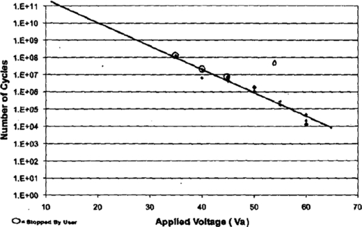
Figure 2. Goldsmith et al [19] were the first to report on the charging-based reliability limitation of capacitive RF MEMS switches. Reproduced with permission from [19]. Copyright 2001 IEEE.
Download figure:
Standard imageIn 2002, Reid [22] presented the first theoretical analysis of the effect of accumulating charge on device behavior, complete with the experimental verification. A numerical model was designed, with which it was possible to calculate the effect of a certain amount of charge in the dielectric on the C/V curve shift of a capacitive MEMS switch. He reasoned that if the positive or the negative pull-out voltage crosses the 0 V line, the switch will fail to pull out, while too high a shift may also cause the actuation voltage to be unable to pull the switch down. This accurately defines the failure mechanism due to charging, loosely referred to until then as a form of 'stiction'; see figure 3.

Figure 3. Reid showed that charging of the dielectric causes a continuing shift of the complete C/V curve, until the switch fails. Figure adapted from [22]. The dotted line shows the initial C/V curve (it is asymmetric around 0 V, so some charge must already be present), while the solid line shows the effect of actuation-induced charge building up.
Download figure:
Standard imageHow this shift of the pull-in and pull-out voltages develops over time was first assessed by van Spengen et al [23]. Until then the reliability of capacitive MEMS switches had been reported in terms of number of cycles to failure, similar to macroscopic relays and metal-to-metal contact MEMS switches. van Spengen et al reasoned that charging is continuously taking place under the influence of the actuation voltage when the bridge is in the down position, while there is no charging when the bridge is not actuated. Only the time that the bridge is down matters, not how often it actually switches up and down during this period, leading to the 'total actuation time to failure' as a new figure of merit (FoM), instead of number of cycles. They proved the point by actuating identical switches to failure by using different actuation frequencies. The number of cycles to failure differed widely, while the total time to failure was the same.
Based on measurements with a dedicated test setup [24], in 2004, van Spengen et al [25] expanded the earlier work of Reid into an analytical model predicting the time to failure. They adapted the earlier analytical work of Wibbeler et al [26] describing charge effects on suspended membranes to include pull-in and pull-out instabilities. The value of a critical amount of charge was calculated, which will just cause the positive or negative pull-out voltage to cross 0 V, hence causing stiction in the way described by Reid [22]. The authors warn against investigating charging behavior with unipolar C/V measurements, as these will not show the failure of the negative pull-out voltage crossing 0 V; see figure 4.
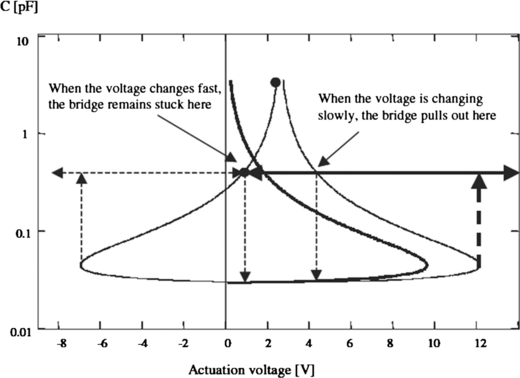
Figure 4. The model of van Spengen et al [25] predicts that a switch will fail in a switching test even though a unipolar C/V curve will not show any problem, because the negative pull-out voltage shifts through 0 V.
Download figure:
Standard imageThe time it takes to attain this critical amount of charge depends on the physics of the charging mechanism. In the van Spengen et al's paper, a simple stretched exponential for charging is introduced, based on similar charging models for MOSFET high-k gate dielectrics. This stretched exponential was quickly confirmed experimentally [27]. The effect of different charging and discharging time constants is discussed, as is the effect of varying duty cycles. An equation is derived that describes the experimentally observed fact that the lifetime goes exponentially down with increasing actuation voltage. Also noted is the fact that partially contacting or partially stuck bridges can cause a non-uniform charge distribution leading to a change in C/V curve shape in addition to a shift of the complete curve. In [23, 28, 29], the same authors show optical displacement images obtained using an interferometer of partially stuck RF MEMS switches subject to non-uniform charging; see figure 5.

Figure 5. Measurement of non-uniform motion by taking the difference of two interferometric images (a) and (b), and a top view SEM (Scanning Electron Microscope) micrograph (c). The non-uniformity in the motion can lead to a spatial charge distribution. Reproduced from [23]. Copyright 2002 IEEE.
Download figure:
Standard imageRottenberg et al [30, 31] also in 2004 presented an analytical model for the effect of this non-uniform charge density. This spatial non-uniformity can be processing related, or appear due to a non-uniform charge injection across the parasitic air gap. They reason that the non-uniformity can be described by its statistical variance, which then can be used as an important parameter to describe the observed narrowing of the C/V curve. This narrowing occurs because several spatially separated areas of the dielectric will exert a different pulling force at different actuation voltages. If the variance becomes too large, the pull-out voltage completely disappears; see figure 6.
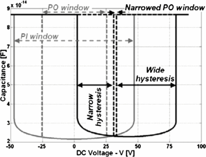
Figure 6. Calculation of the shift and narrowing of a C/V curve by non-uniform charging by Rottenberg et al [31]. The grey lines show the starting C/V curve without charging, the black lines give the C/V curve just before the non-uniform charge distribution causes the device to loose the possibility to pull-out at any voltage. PI = pull-in, PO = pull-out. Reproduced from [31]. Copyright 2007 IEEE.
Download figure:
Standard imageYuan et al [32] added the notion that the shift in voltage is linear in the charge, and hence, the change in pull-in and pull-out voltages can be directly related to the charging taking place. This was later used in the concept of the shift rate of actuation voltages (SRAV).
From here on, people have worked on several different aspects of the charging problem. One direction was the more in-depth study of the effect of (distributed) charge on device behavior, presented in section 2.2. Other research focused on the development and characterization of better-performing dielectrics from a reliability point of view in section 2.3. A further approach was the investigation of advanced actuation waveform concepts that minimize charging and other adverse effects in section 2.4. The mechanical design was improved to achieve higher restoring forces, lowering the chance of stiction in section 2.5. Finally, the radical departure from the original geometries to try to prevent charging by introducing new device concepts with no dielectric is covered in section 3.
2.2. The effect of charging on device behavior
Melle et al [33, 34] noted that if a good model for the uniform accumulation of charge during operation is available, the devices need not to be tested completely to failure to assess their expected lifetime. The rate of shift of the C/V curve can be measured for a short time, and the total lifetime extrapolated from this data set. As the key parameter they introduce the SRAV. This shift is linear in the accumulated charge and experimentally fits with calculation of Poole–Frenkel-induced charging as a function of actuation voltage; see figure 7. They normalize the SRAV with respect to the electrical stressing condition and hence obtain a FoM for the intrinsic charging behavior of the dielectric, irrespective of the details of the switch. With this, they compare different dielectrics reported in the literature (higher is better, and one decade of extra FoM gives one decade of extra lifetime under the same actuation conditions); see figure 8.

Figure 7. The SRAV corresponds with predictions from Poole–Frenkel charging theory [33]. Dv/Dt is the rate of shift of the C/V curve. Two switches with different dielectric thicknesses of 0.2 µm and 0.28 µm were used. Reproduced from [33]. Copyright 2005 IEEE.
Download figure:
Standard image
Figure 8. Illustration of the comparison of different quality dielectrics with respect to charging based on the FoM figure of Melle et al [34]. Bipolar actuation is covered in section 2.4. Reproduced from [34]. Copyright 2005 Elsevier.
Download figure:
Standard imageA complication in C/V curve shift measurements is that measuring the C/V curve itself takes time and may charge the dielectric, thereby introducing a significant measurement error. Herfst et al [35, 36] show that by a careful capacitance measurement around 0 V, the shift can be measured without actually fully actuating the switch and pulling the bridge down; see figure 9. By fitting a parabola to the measured curves, the shift can be extracted very accurately. The C/V curve narrowing due to non-uniform charging also has an influence.

Figure 9. Herfst et al [36] measure the shift of the C/V curve during a switching reliability test without actually stressing the dielectric with extra C/V curves. They measure the shift of the minimum capacitance to predict changes in the total C/V curve. Reproduced from [36]. Copyright 2008 IEEE.
Download figure:
Standard imagePapaioannou et al [37] however observe a shift of the C/V curve with the technique of Herfst et al [35] even if there is no pull-in at all during the experiment. They attribute this to a polarization of the dielectric over time under the influence of the electric field. Czarnecki et al [38, 39] attribute the charging time constant they obtain in addition to the 'normal' dielectric charging to charges accumulating between the conductors in the substrate. It is not quite clear from the papers whether these two different effects can always be properly distinguished. The substrate charging has also recently been observed in dielectric less switches; see section 3.2. Kelvin probe force microscopy (KPFM) clearly shows charge accumulating outside the capacitor area but still in the dielectric [40, 41], and it should be possible to also map the charging susceptibility of the substrate itself using this technique.
In Matmat et al [42, 43], the important notion is made that as the Poole–Frenkel conduction is a temperature-activated process, charging is more problematic at higher temperatures. This was experimentally verified (figure 10). Zhaglul et al [41] in addition warn about the effect of humidity. They show that a high humidity results in more charging of the (SiNx) dielectric, but that the electric field also enhances the formation of a water meniscus between the dielectric and the bridge. They argue that this meniscus has an influence on the adhesion force in the form of an 'electric field enhancement' of classical stiction due to a capillary condensate [44, 45].

Figure 10. A higher temperature results in faster charging. Reproduced from [43]. Copyright 2010 Elsevier.
Download figure:
Standard image2.3. The development and characterization of high-performance dielectrics
In the early capacitive RF MEMS switches, the dielectric was SiNx, see, e.g., [17, 46]. SiNx has a reasonably high dielectric constant and is readily available in many semiconductor processing facilities. However, it suffers heavily from the charging phenomenon.
It was recognized early on that a suitable dielectric should either be so 'perfect' that no significant charging can take place during the operational life of the device, or it should be so leaky that accumulated charge leaks away immediately upon the removal of the stressing voltage, as described in a Texas Instruments patent [47]. Many materials have been evaluated for their suitability as an RF MEMS switch dielectric, such as several types of SiNx [40, 41, 48–52], SiO2 [53, 54], high-k dielectrics, such as Ta2O5 [55, 56] and HfO2 and oxynitride [57, 58], a composite dielectric with carbon nanotubes (CNTs) in SiNx [59], and even nanocrystalline diamond (NCD) [60] and ultrananocrystalline diamond (UNCD) [61].
While many tests with dielectric materials have been 'trial and error', other studies have been more systematic and have resulted in an important knowledge base for the study of dielectric charging. Despite our increased knowledge of the charging behavior of dielectrics under high-field stressing, the ideal dielectric has not yet been developed. However, the adverse effects of charging can be reduced to the point that quite reliable switches have been produced, such as those described by Goldsmith et al [54], which can be operated for over 100 billion cycles at 60 kHz switching frequency with no failures under optimized actuation conditions. The dielectric of these switches is made up of sputtered SiO2, resulting in high reliability but low on-state capacitance to off-state capacitance (Con/Coff) ratio, due to the low dielectric constant of SiO2.
Two main mechanisms can contribute to dielectric charging, being polarization and charge injection. Within this classification, many phenomena occur. Orientational (or dipolar) polarization, space–charge polarization, interfacial polarization and internal charge migration all can contribute to polarization. External charge injection can consist of contributions by trap-assisted tunneling (TAT), Poole–Frenkel conduction and Schottky (or thermal) emission from the conductor directly in the dielectric. The Fowler–Nordheim tunneling, which was proposed in the earlier literature, is not expected to be significant at the field strengths encountered in capacitive MEMS switch dielectrics during normal operation. A comprehensive overview of the different charging phenomena is given by Papaioannou [61].
The three most important experimental techniques to assess the quality of the dielectric with respect to charging are (1) low-level current measurements with metal–insulator–metal (MIM) capacitors, (2) thermally stimulated discharge/depolarization current (TSDC) measurements and (3) KPFM. It should be stressed that techniques based on MIM capacitor measurements inherently neglect the important effect of top surface charging, where the charge stays at the surface of the dielectric [54].
2.3.1. Low-level leakage current measurements
As the accumulation of charges within the dielectric is related, and sometimes even proportional, to the leakage current [34], it is possible to assess the quality of the dielectric by measuring the leakage current as a function of stressing voltage in a MIM capacitor configuration. The leakage current typically shows the Poole–Frenkel behavior at high fields, but other conduction mechanism can be present as well at lower fields, such as TAT. A recent example of a MIM capacitor leakage current measurement is given in figure 11. It is also possible to directly measure the charging current as a transient current on top of the leakage current (figure 12).
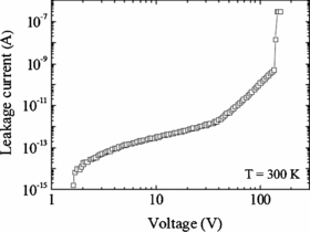
Figure 11. Leakage current measurements with MIM capacitors can reveal different conduction mechanisms at different field strengths by a change in slope. In this case, at low fields TAT is observed, and at high fields Poole-Frenkel conduction. Reproduced from [58]. Copyright 2011 SPIE.
Download figure:
Standard image
Figure 12. Stressing the dielectric with a square wave actuation reveals the charging and discharging transients themselves if the current measurement resolution is high enough. Reproduced with permission from [62]. Copyright 2008 Elsevier.
Download figure:
Standard image2.3.2. TSDC measurements
TSDC has been in use for a long time to study charge retention of dielectrics. In the past, it was used, e.g., for the assessment of the longevity of electret microphones [63]. It has been applied successfully to investigate the nature of the traps in RF MEMS switch dielectrics [48].
A TSDC experiment is performed by first charging the dielectric in a MIM capacitor configuration, and then monitoring the discharge current while the temperature of the dielectric is ramped up. In this way, all charge trapped with a certain activation energy will be released when the ramp reaches the corresponding temperature. This allows a detailed investigation of the distribution of trap site energies. A recent example is given in figure 13, showing a graph of the discharge current and the total charge as a function of temperature for a number of PECVD SiNx dielectrics with different stoichiometry.

Figure 13. TSDC experiment revealing the amount of charge and the activation energy of the trapping sites in different SiNx dielectrics. The insert shows the measured current ITSDC that flows while ramping up the temperature, while the main figure shows the corresponding charge Qext extracted from three different dielectrics A, B, and C. Two different trapping energies at 0.20 eV and 0.83 eV are identified in this plot. Reproduced with permission from [48]. Copyright 2011 American Institute of Physics.
Download figure:
Standard image2.3.3. KPFM measurements
KPFM is a technique based on atomic force microscopy (AFM) with a conductive tip. After a normal AFM scan has been performed to obtain the surface topography, a voltage is applied to the tip, and the local electrostatic force can be assessed while scanning. In this way, surface maps of the charge can be produced. It is also possible to inject charge with the tip itself, mimicking a single asperity contact of the MEMS switch bridge touching the dielectric. The amount of charging, and its spatial and temporal evolution can then be studied in detail. A recent example of the evolution study of charge on a SiNx dielectric is given in figure 14.

Figure 14. The evolution of positive injected charge at 20 V over time on an SiNx dielectric, measured by KFPM. Reproduced with permission from [40]. Copyright 2011 American Institute of Physics.
Download figure:
Standard imageThe discharge current can also be directly measured as a change of the midpoint capacitance of Herfst et al [35], even over long times ∼104 s. This technique has an equivalent sub-fA range sensitivity [64]. Both SiO2 and SiNx have been shown to be susceptible to additional trap formation with long time constants under the influence of ionizing radiation, increasing the stiction problem [52]. This is an issue to consider when RF MEMS switches are to be applied, e.g., in space. An optical technique borrowed from MOSFET dielectric studies can be used to extract both the charge magnitude and the depth distribution [65], but has not yet been widely adopted in RF MEMS switch research.
Table 1 summarizes the most important insights into the charging of different dielectrics that have been obtained using the techniques discussed above.
Table 1. RF MEMS switch dielectrics and their charging behavior.
| SiO2 | Can be sputtered as a relatively high-quality amorphous film, resulting in high-reliability devices [54]. εr ≈ 4.5 only, so Cdown/Cup is limited. The charging time constants are independent of temperature, while the attainable 'steady state' amount of charge follows an Arrhenius relation. The leakage current also increases with temperature, but the net effect of a higher temperature is the worsening of the overall charging properties due to the large amount of available traps [66]. Polarization charging is always present, while there is a voltage threshold for charge injection [53]. |
| SiNx | Most commonly used dielectric material, εr ≈ 7.5. Plasma-enhanced chemical vapor deposition (PECVD) is typically used, and films with different stoichiometry can be obtained, with N/Si ratios ranging from 0.36 to 0.85. Silicon-rich films (low temperature and/or low plasma frequency deposition) show both more charging and more leakage current [50], but their overall performance is reportedly worse [48], contradicting an early patent on leaky dielectrics [47]. Thin films have a longer charging time constant than thicker films, and whether the conductor below the SiNx is silicon or a metal influences the charge-recollection behavior [49]. Also, it was experimentally proven that thicker films can store more total charge [67]. Trapped charge polarity can be either positive or negative in the same traps (basically they are dangling bonds inside the material) [27]. This is probably also generally true for all of the discussed high-k dielectrics. However, although the trapping and decay time constants are of the same order for both charge polarities, they are not exactly equal and depend on the material below the dielectric [40]. Charging is also higher in a high-humidity environment [41]. Infrared spectroscopy has revealed that a low hydrogen content in the SiNx film leads to a higher leakage current and a shorter discharging time constant [51]. |
| Ta2O5 | High-k dielectric with εr ≈ 32 can be made by RF magnetron reactive sputtering of a Ta target with an Ar/O2 background pressure. The charging time constant and stretch factor of the exponent change as a function of applied field [55]. A kink is observed in the leakage current versus field curve at medium fields, below which the leakage current is more or less proportional to the field (TAT), and above which a fast increase is observed (Poole–Frenkel) [56]. |
| HfO2 | A HfO2/PZT bilayer dielectric has shown a 103 times lower leakage current than SiNx, with a combined stack εr ≈ 80 [58]. No switch reliability tests were reported for this configuration. |
| HfOxNy | Film created by reactive sputtering, εr ≈ 19. More resistant to crystallization than HfO2 and hence a higher mechanical reliability. High breakdown strength in MIM capacitors. Prepared device failed by breakdown of the dielectric at the edges due to poor step coverage [57]. |
| CNT in SiNx | SiNx dielectric composite material with multiwall CNTs inside the SiNx layer, εr ≈ the same as for SiNx alone. The leakage current is higher, and an improvement of two orders of magnitude in lifetime is claimed over normal SiNx [59]. |
| NCD | NCD is used as a leaky dielectric, and εr ≈ 5. The leakage current is typically two orders of magnitude higher than SiNx. No switch reliability was reported [60]. |
| UNCD | UNCD, εr ≈ 5.2, is even leakier than NCD, about five orders of magnitude more than SiNx. Switch charges fast, but as the discharging time is only ∼50 µs, it can be operated near-continuously, as long as the maximum single-cycle hold time is observed [61]. |
| BCB | Benzocyclobutene, used in flexible PCB-based switches, can be used as part of the board material itself, and hence possibly results in very cost-effective switches. If breakdown is prevented by polishing the substrate, no failures are observed. Switches described are much larger than usual, and the dielectric thickness is 2.5 µm [68]. |
| Others | More dielectrics are used, such as, e.g., AlN (a wide bandgap semiconductor) [38], SiOxNy [18], SrTiO3 [69], and BaSrTiO3 [70], and are well worth further investigation. |
2.4. Advanced actuation waveforms
Because the charging issue was already clear from the early switches, more advanced waveforms than a simple square wave actuation have been routinely applied throughout the capacitive MEMS switch development. Goldsmith et al [19] already used a high-voltage pulse to pull the bridge down, and a lower 'holding voltage' to keep charging to a minimum. Because both positive and negative actuation voltages can be used to pull the bridge down, bipolar actuation has the advantage that (part of) the charge built up during the positive actuation cycle can be removed during the negative cycle [71]. Bipolar actuation can be used on a switch cycle-to-cycle basis, or the polarity can be swept during actuation, if the transition is much faster than the switch can follow mechanically due to its limited resonance frequency, experimentally used in [72]. The latter solution has the advantage that it enables the possibility of keeping the switch in the down position continuously, but has higher power consumption because the capacitor constituting the switch has to be charged and discharged more often than if a single pulse is used (figure 15).

Figure 15. Traditional actuation waveforms for capacitive RF MEMS switches [73].
Download figure:
Standard imageA SPICE model of the charging behavior can be used to predict how different actuation waveforms will change the charging behavior [74]. Peng et al [75] have thoroughly investigated both theoretically and experimentally how well the bipolar operation is able to cancel the charging taking place in SiO2. Although a large improvement is certainly achieved, complete cancellation is difficult due to the fact that positive and negative charging and discharging processes are not exactly equal and are dependent on the stressing conditions; a fact that was also observed by Zaghlul et al [40] in their study of SiNx properties. Czarnecki et al [38] also observe actuation voltage-dependent behavior under bipolar actuation with an AlN dielectric, in this case also due to several charging mechanisms competing at the same time. They conclude that depending on the material and stressing conditions, bipolar actuation is not always advantageous. They also note that even though bipolar actuation can prevent a shift of the C/V curve, a non-uniform charge distribution leads to narrowing of the C/V curve and, eventually, still to failure.
Actuation pulse shaping can be used to tailor the charging behavior, but also applied to optimize the mechanical motion of the bridge upon pull-in and pull-out. Although optimizing the pressure in the zero-level package can make the switch move in a critically damped fashion (see section 4.3), electric tailoring can also be convenient. First of all it must be noted that while a low holding voltage is advantageous for low charging, the resulting force on the bridge will be lower, resulting in a less intimate contact between the bridge and the dielectric. This in turn results in worse RF behavior in the down state, in the form of a lower Con. Also, although a higher actuation voltage makes a switch turn on faster, it can also result in bouncing if the impact force is too high [76].
The first application of a complex tailored waveform, for Ohmic switches in this case, was presented in 2006 by Czaplewski et al [77]. Using finite-element modeling (FEM) and laser Doppler vibrometry experiments, the same group (Sumali et al [78]) optimized a waveform consisting of a short high pulse, just enough to move the switch down, and a low, longer holding force pulse (figure 16). The shape and amplitude of the high pulse is ideal, when the bridge moves down as quickly as possible, and still the velocity of the bridge just reaches zero at the moment of contact. Rounding the first pulse is also advantageous for smooth motion. No bouncing will occur with such a pulse, and the mechanical lifetime will be extended.

Figure 16. Optimizing the shape, time and amplitude of the actuation pulse allows for a 'soft landing' with no bouncing effects. Reproduced with permission from [78]. Copyright 2007 Elsevier.
Download figure:
Standard imageIn [79], a similar, slightly less elaborate approach is taken, with the interesting notion that rounding the actuation waveform experimentally results in less charging. As the bridge is not contacting the dielectric during this pulse, this means that the polarization of the dielectric and/or the substrate charging behavior is modified. Tazolli et al [80] show with their simulations and measurements that while it is possible to design a waveform for low bouncing when the bridge is pulled down, an underdamped switch will also freely (almost) bounce and resonate significantly when released, as already experimentally observed in [81]. It is possible to electronically stop this release-related motion. Spasos et al [82] have shown that it is possible to optimize the type of pulse shape advocated in [78] by adding one or more tailored pulses at the end of the actuation cycle, using Taguchi's method, to stop the resonance ring down upon release; see figure 17.
Figure 17. Adding the right type of actuation pulses after the release has taken place prevents the ringdown of underdamped devices, which can speed up the mechanical switching time performance. Reproduced with permission from [80]. Copyright 2010 Springer.
Download figure:
Standard image2.5. Mechanical design improvements
The most pragmatic way to reduce charge-induced stiction within the 'standard' capacitive RF MEMS geometry is by noting that if the restoring force is insufficient to release the bridge, it should be made higher, or the area of the dielectric should be made smaller.
Increasing the bridge film thickness and shortening its length obviously makes it stiffer, and hence results in a higher restoring force. However, the actuation voltage also increases as a result (which has a nonlinear influence on the charging), making that the overall robustness of the device against charging decreases for stiffer designs. It is better to use a short cantilever with a wide electrode area so that a low actuation voltage can be maintained, even though the larger actuator presents more surface area for stiction [82].
In [83], bent sides are introduced, effectively changing the bridge into a U-shape, stiffening it substantially without increasing the inertia much. This results in a higher restoring force, which can be used to combat charge-induced stiction. In addition, one obtains very fast switches; reported is a 25-fold increase in resonance frequency over non-U-shape devices. Impressive switching times in the range of 150–400 ns are reported for this configuration.
Goldsmith et al [54] trade the capacitor area for reliability. By using dielectric studs instead of a continuous film, the area susceptible to charging is reduced while the initial pull-down force is basically maintained. A disadvantage is the reduction in Con/Coff, but reliability is much improved.
Lakshminarayanan et al [84] argue that extreme miniaturization of RF MEMS capacitive switches is advantageous, because the scaling laws dictate that the pull-up force per capacitor area then increases while the required actuation voltage remains the same. In their case, the bridge is 20 × 9.5 × 0.37 µm3 only, suspended 0.25 µm above the dielectric. Many of these devices can be simultaneously used in the array form to increase the total capacitance change. As in the case of the U-shaped beams, very fast switching times are possible, in the range of 200 ns, and the devices survive over 20 billion cycles at 50 kHz, 50% duty cycle, bipolar actuation, with no failure. The C/V curve shifts are not given; so, the extent to which these devices are prone to charging is not easily judged.
As a general remark, one can state that a low actuation voltage is advantageous, as the charging problem becomes exponentially more cumbersome at higher voltages, while the spring of the bridge is (roughly) linear. However, too low actuation voltages should be avoided, as very compliant mechanisms are then required. In such a case, one may introduce more problems, such as capillary and molecular-force-induced adhesion [44]. At which point these additional problems will become important depends on the contacting surface properties and switch environment.
3. New device concepts with no dielectric
3.1. Dielectric-less switches
The conclusion of section 2 must be that, even after 15 years of intensive capacitive RF MEMS switch research, the charging issue has all but been solved. Different dielectrics and deposition methods have been investigated, different mechanical configurations have been proposed, and a great deal more is known about the physics of the charging mechanisms now. But except of the approach of extreme further miniaturization, no real solution has emerged. In principle, reliable switches can be manufactured with the (high) actuation voltage present across the dielectric, but in practice the set of requirements on the applied dielectric is so severe that it is exceedingly difficult to produce reliable devices with a high Con/Coff ratio that are easy to handle and can operate under a wide range of stressing conditions. The fact that several charging mechanisms of both polarities are competing and need all to be solved simultaneously, and the effect that charging becomes even worse at higher temperatures; both pose a tremendous reliability challenge.
It is for this reason that the use of switches has been proposed, where no actuation voltage is applied over the switch dielectric at all. The solution can take the form of separating the RF signal and actuation electrodes, and/or leaving out the dielectric altogether and relying on an air gap for the main signal capacitance instead.
Capacitive switches with separated, lowered actuation electrodes were first proposed by van Spengen in 2004 [85], but not actually built (figure 18). In this case, the main device has the same geometry as a normal capacitive shunt switch, but extra electrodes are present on the sides, of which the height is lower than that of the dielectric, a 'recessed relay' configuration. When the bridge is pulled down, it lands on the dielectric, shunting the RF signal, but at the same time, there is still an air gap from the bridge to the actuation electrodes. Hence, the actuation voltage is not stressing the dielectric. Only the RF signal itself, which is much smaller in amplitude, can give rise to some charging in the dielectric. Care has to be taken that the RF properties are not altered by the extra electrodes, but they can be capacitively decoupled to RF ground if required, as they carry only a (quasi-) dc voltage.

Figure 18. The first published capacitive switches concept with separated, lowered actuation electrodes; (a) top view [85], and (b) cross-section along the bridge.
Download figure:
Standard imageWith many refinements, this concept was later implemented in practice by Grichener and Rebeiz [10]. They use a very thick single-side clamped cantilever as the bridge, which touches in a single line upon pull-in and can be folded further by increasing the actuation voltage or a bias on the signal line, resulting in some capacitance tenability as well as the main instability (figure 19). With a normal 150 nm PECVD SiNx dielectric film and a substantial actuation voltage of around 50 V for different geometries, they achieve excellent reliability. Some shift of the pull-in and pull-out voltages is observed, but the switches easily survive with no failures for hours in a switching test (figure 20). Projected lifetimes based on the voltage shifts are, depending on duty cycle, tens to hundreds of days for unipolar actuation, and tens to hundreds of years for bipolar actuation!

Figure 19. Dielectric-less actuation switch [10] with dielectric on the signal line for high Con/Coff. The numbers are dimensions in µm. Vs is the voltage on the actuation electrode, while an extra holding voltage Vh can be applied under the dielectric; g0 is the initial gap height, tb is the bridge thickness, and td is the dielectric thickness. Ports 1 and 2 are the two RF signal lines. Reproduced with permission from [10]. Copyright 2010 IEEE.
Download figure:
Standard image
Figure 20. The separation of a recessed actuation electrode and signal electrode of the switch leads to a high-reliability device with projected bipolar operation lifetimes of tens to hundreds of years [10]. Vpi = pull-in voltage; Vr = release, or pull-out, voltage. Reproduced with permission from [10]. Copyright 2010 IEEE.
Download figure:
Standard imageShortly after [85], Blondy et al [86] reported on the first dielectric-less switches where the dielectric is left out altogether. Instead, the bridge is shaped such that it does not touch any of the electrodes underneath when pulled in (figure 21). Although the switch drawn here has separate actuation electrodes, the main advantage of this configuration can be found in the fact that RF and actuation can still be combined into one electrode, making the resulting device potentially smaller than the devices discussed before.

Figure 21. The device of Blondy et al [86] contains no dielectric that can charge at all. Figure (a) shows a conventional shunt switch cross-section, and (b) the device without dielectric. Reproduced with permission from [86]. Copyright 2004 IEEE.
Download figure:
Standard imageThe susceptibility to charging is greatly decreased but has not completely vanished, as shown with switches with a single-sided clamped beam [87, 88]. The residual charging is associated by the authors with wafer substrate charging. Figure 22 shows the shift of the pull-in voltage for unipolar and bipolar actuation, resulting in a 20 V shift after a month for unipolar actuation (with a 60 V pull-in voltage), and tens of years for bipolar actuation, comparable to [10]. A similar configuration, with separate stopper dimples landing on grounded lines and many electrodes was later used by van Spengen et al [89] in the demonstration switches for a purely MEMS-switch-based pulse width modulation (PWM) amplifier, the 'MEMSamp'; see section 3.2.

Figure 22. The low charging of a switch with no dielectric at all also results in a lifetime prediction of tens of years under bipolar actuation [88]. Pull-down = pull-in voltage. Reproduced with permission from [88]. Copyright 2009 IEEE.
Download figure:
Standard imageIn a quest to make the devices even more reliable, Lu et al [90] propose to dispense with the switching mechanism as well, instead of relying on the limited Con/Coff ratio of a tunable MEMS varactor. This ratio before pull-in can be increased with a clever dual beam approach. The authors specifically recommend this design for high-RF-power applications and demonstrate operation at 4 W. Self-actuation is a problem for high powers, and the actuation voltage needs to be reduced in accordance with the momentary signal power. Park et al [91] are also in favor of a non-switching configuration. They use rather slow and bulky comb-drive actuators to shunt the co-planar waveguide (CPW) center conductor from the sides. In this way, there is no pull-in instability and Con/Coff can be large.
A small discussion is appropriate here. With dielectric-less switches, it seems it is far easier to achieve devices that suffer relatively little from charging than with conventional devices. The devices presented in the literature so far however have a limited Con/Coff ratio, being 5–9 in [10] and 5 in [88]. For the completely dielectric-less switch, this low Con/Coff is a fundamental limitation, which can only be partly circumvented by tricks, such as presented in [90]. When one allows for a dielectric on top of the signal line, as in [10], high-k dielectrics, such as Ta2O5 or HfO2, can still be used to achieve a high Con/Coff, without the associated charging and leakage–current-induced breakdown.
The RF signal in this case is present across the dielectric, which in principle makes that the RF signal can play the same role as a bipolar actuation voltage as far as the charging process is concerned, even though the voltage amplitude is lower. This may result in a limited amount of signal-related charging of the dielectric. Its effect can easily be estimated. The total voltage shift due to signal charging can never be higher (positive or negative) than the voltage that caused it. A safe limitation is then that the instantaneous RF signal voltage should always be less than half the pull-out voltage Vpo minus a small safety margin. In this way, the pull-out voltage can never shift far enough to make the bridge stick by self-actuation (figure 23). This is a more stringent criterion than using the self-actuation point as the maximum allowable signal voltage amplitude, but will result in a high-reliability device.
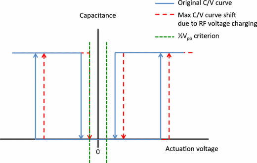
Figure 23. Graphical explanation of the 1/2 Vpo criterion for the RF voltage. If the maximum RF voltage is taken equal to Vpo, the bridge will stick in the presence of this power as soon as some charging-related C/V curve shift occurs. Only by specifying the maximum RF voltage such that if will not keep the bridge down by self-actuation at the maximum RF-related voltage shift possible, the device will be reliable with respect to charging. This is the point for which the sum of the self-actuation voltage and the maximum shift voltage (which are both the same as the RF voltage) equals the pull-out voltage, so 2 VRF = Vpo.
Download figure:
Standard imageUsing these dielectric-less switches, the only issue remaining to be dealt with in order to obtain a fully reliable capacitive RF MEMS switch with respect to charging is substrate charging, discussed in the next section.
3.2. Electrostatic screening of the accumulating substrate charge
Substrate charging is commonly seen in high-resistivity substrates. It is very obvious in glass wafers and, to a lesser extent, in high-resistivity silicon [92]. Although it is a dominant factor in dielectric-less switches and metal-to-metal contact switches [93], it has also been observed as one of the charging contributions in regular switches [38]. It can even shift the resonance frequency of MEMS resonators [94]. Czarnecki et al [39] have shown with identical switches with and without dielectric that substrate charging is a major effect. It is in regular switches not always evident whether a non-contact charging effect must be attributed to non-contact dipole orientation and/or intrinsic free-charge migration, or substrate charging. This is a complicating factor for the study of these devices and makes it difficult to judge whether the effect is present in non-contact measurements, such as, e.g., those of Papaioannou et al [37].
In dielectric-less switches, substrate charging is the only really dangerous contribution. Assumed locations of the charge accumulation are under the stoppers [85] (see figure 24) and between the actuation electrode and the ground and signal electrodes [10] (see figure 25).
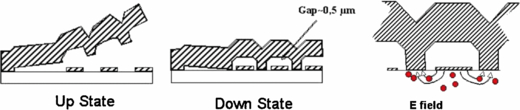
Figure 24. The switch of Mardivirin et al [87] lands directly on the substrate, and can hence suffer from charge accumulation by charges migrating from the actuation electrode. Reproduced with permission from [87]. Copyright 2008 IEEE.
Download figure:
Standard image
Figure 25. In a switch with dielectric on the signal electrode and separate voltage Vs on the actuation electrode, the main charge accumulates in the substrate, but an additional holding voltage (Vh in the figure) or the RF signal itself can still contribute to a charge in the dielectric. Reproduced with permission from [10]. Copyright 2010 IEEE.
Download figure:
Standard imageIn both cases, it is straightforward to physically describe the effect of charging on device performance, because there is only one dominant contribution. Both groups fit the voltage shifts to the Curie–Von Schweidler equation:

where ΔV is the pull-in voltage shift, Q is the trapped charge, t is the time, and k, A and n are constants. This empirical equation describes charging well over the times observed, but it would be interesting to see the fit to the stretched exponential law (also called the Williams–Watts–Kohlrausch relaxation law) as well. Extrapolating the prediction of voltage shifts to such long lifetimes as tens or even hundreds of years without a solid theory to complement the observed empirical laws is not without risk. More research is certainly required here, both theoretically and experimentally.
This leaves the question whether the charge accumulating in the substrate cannot be electrostatically screened by extra ground planes. The charge does not accumulate in the path of the main signal flow, and can hence be (at least partially) screened. The first screening solution has been given in 2002 in a paper by Rottenberg et al [95]. They were concerned with traditional capacitive switches with dielectric, but a metal layer was deposited on top of the dielectric to screen the accumulating charge from the bridge (figure 26). In addition, this configuration allows one to obtain a much higher capacitance ratio, as there is no air gap between the bridge and the dielectric due to the inevitable surface roughness. However, the actuation and holding mechanism is complicated [96], and the contact of the bridge with the metal layer on top of the dielectric can suffer from typical metal-to-metal switch degradation mechanisms; so, this switch configuration has not been widely used so far. Still, this is the first example of a capacitive RF MEMS with a charge screening solution.
Figure 26. Rottenberg et al [95] screen the charge accumulating in the dielectric with an extra metal plate. Reproduced with permission from [95]. Copyright 2002 IEEE.
Download figure:
Standard imageThe problem of charge accumulation below the bridge stoppers given in [87] (see figure 24) can be partly circumvented by having them land not directly on the substrate, but on a dedicated grounded electrode. This grounded landing electrode solution has been reported by van Spengen et al [89] (see figure 27) even though their devices are strictly speaking not RF switches (they are made up of polycrystalline silicon).
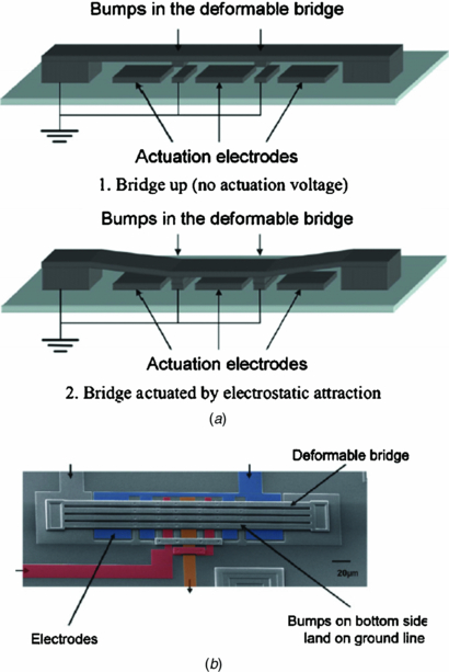
Figure 27. In the switches for the MEMSamp, adapted from [89], the bridge lands with stoppers on a grounded electrode, preventing charge build-up at the landing site.
Download figure:
Standard imageAdditional charge can still accumulate between the electrodes. This has also been observed in MEMS-based scanning probe microscopy (SPM) scanners [97, 98]. These scanners are basically dielectric-less switches that are not supposed to be pulled in. The suspended membrane plate constitutes a MEMS varactor with the electrode below it. Early versions suffered from some charge accumulating around the actuation electrode, which limits the repeatability of the motion. In these devices, this is not such a problem now, as long as the actuation voltage is kept below 30 V. However, capacitive crosstalk between the actuation electrode and the sample to be measured, which is to be positioned close to the moving plate, limits the maximum operating frequency in scanning tunneling microscopy (STM) applications [98]. For this reason, extensive screening was applied at the sides, not to screen the bridge from accumulating charge, but to screen the surroundings from the electric fringe field of the actuation electrode (figure 28). A similar approach with screening under the bridge—instead of on top—would possibly render the last reminiscent substrate charging effects insignificant and constitute the last ingredient for a capacitive RF MEMS switch that does not suffer from any form of charging. Figure 28 shows a solution, which would also automatically result in a U-shaped bridge profile.
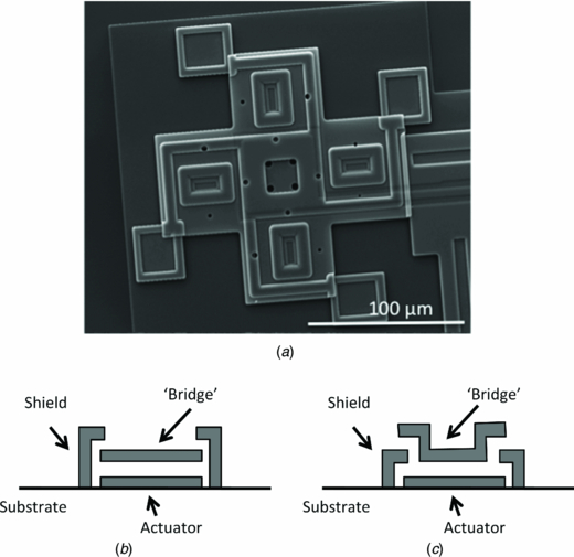
Figure 28. In MEMS STM scanners, the fringe field of the actuator is screened from the surroundings (an and (b)). A similar approach with shield under the edges of the bridge instead of above the edges could be taken to prevent the substrate charging effect from influencing the bridge motion (c).
Download figure:
Standard imageIt is expected that the application of this kind of electrostatic screening in combination with dielectric-less switches should be enough to render any dielectric charging insignificant from a device reliability perspective.
4. Other failure mechanisms
In this paper, charging has been treated extensively, as it is the 'show-stopping' failure mechanism for capacitive RF MEMS switches. That is not to say that there are no other important failure mechanisms. However, with clever conventional engineering in the early stages of the design, these do not need to become a fundamental reliability hazard. In this section, creep, high-power effects and packaging-related issues are briefly discussed. High-cycle fatigue of the bridge is not to be expected for thin-film devices because there are too few defects that can migrate to the surface of the bridge under cyclic stress to form continuous cracks [99]. Fatigue in capacitive RF MEMS switches has indeed never been observed [100].
4.1. Creep
Creep is the time-dependent relaxation of a material under mechanical stress by plastic deformation. It is not present in crystalline brittle solids, such as silicon, and is hence not often observed in the general MEMS field. RF MEMS switches need a highly conductive moving bridge, as the RF performance rapidly deteriorates with increasing electrical resistance. Many RF MEMS switch designs employ bridges out of aluminum, because it has a high conductivity, can be easily grown in smooth films and forms a thin protective native oxide that prevents further oxidation in ambient air (in contrast to, e.g., copper, which is also very conductive).
Macroscopically, creep is hardly observed if the temperature is kept below 0.3 times the melting temperature of a ductile metal, but at 0.4 times it is already worth a significant investigation, and above 0.5 times the melting temperature it typically leads to rapid failure (figure 29). Aluminum has notoriously bad creep properties, and there are indications that creep occurs even more in thin films than in bulk material [99]. Texas Instruments has recognized early on in the development of the digital micromirror device (DMD) that flexure hinges made of pure aluminum are unsuitable and lead to a 'hinge memory effect' [101]. They remedied this by applying a creep-resistant aluminum alloy [102].

Figure 29. Creep in metals as given by the temperature-dependent part of the strain ε is a function of the ratio between room temperature T and the melting point Tm and the applied mechanical stress σ. Reproduced with permission from [99]. Copyright 2003 Elsevier.
Download figure:
Standard imageDedicated public studies on creep behavior of RF MEMS bridge materials are scarce. Modlinksi et al [103, 104] performed an extensive study on a comparison of the creep properties of pure aluminum and a number of alloys, such as Al98.3Cu1.7, Al 99.7V0.2Pd0.1 and Al93.5Cu4.4Mg 1.5Mn0.6. The latter turns out to be very creep resistant (figure 30). In addition to melting point effects, an important inhibition mechanism for creep is the presence of immobile, hard precipitates in the film (figure 31).

Figure 30. Wafer-bending experiments showing the creep relaxation of different deposition-induced pre-stressed alloys at 87 °C. Reproduced with permission from [103]. Copyright 2004 Elsevier.
Download figure:
Standard image
Figure 31. This TEM (transmission electron microscopy) micrograph shows the small creep-inhibiting precipitates in Al93.5Cu4.4Mg 1.5Mn0.6. Reproduced with permission from [103]. Copyright 2004 Elsevier.
Download figure:
Standard imageVan Gils et al [105] have shown with FEM the effect of creep on capacitive RF MEMS switch behavior, but they find large differences between the simulations and experiments, maybe due to (surface) charging.
Apart from aluminum bridges, several other materials have been used, such as the high melting point metal molybdenum [106] and creep-resistant ultrafine crystalline nickel [107], among others.
Bilayers consisting of a creep-resistant material can also be advantageous, such as in the case of [91], where copper is deposited on an SOI structure. Gold on silicon [89] also has excellent mechanical properties. Preferably, the high-conductivity layer should be the bottom one of a stack to prevent seeing the electronic influence of the creep resistant layer in the RF performance. However, Patton and Zabinski [108] find that prolonged contacting stress of a metal touching the dielectric contact can lead to increased adhesion due to the deformation of the contacting asperities by creep. This means that an increasing stiction force can even occur with no actuation voltage, and hence no charging at all. This effect would favor a hard (metal) layer for the lower side of the bridge. Alternatively, the insulating dielectric can be used as the creep-resistant structural layer being a part of the bridge, as demonstrated in the case of insulating SiC bridges with a thin Cr/Au layer on top [109]. With careful design though, aluminum alloys could be acceptable, as shown by the DMD. High-temperature tests are mandatory in that case.
4.2. Self-actuation (signal/shock) and RF-power heating
Similar to the fact that high current and voltage have an influence on metal-to-metal contact switch reliability, the capacitive RF MEMS switch behavior is also altered by high-power switching. The most obvious effect is that the RF voltage will exert a force on the bridge in addition to the actuation voltage, and high RF levels can keep the bridge in the down position (acting as the 'holding voltage') or even actuate the switch [110]. The maximum RF-power specification allowed to prevent this latching is a reliability issue as this maximum RF-power level becomes lower when charging of the dielectric occurs.
Due the finite inertia of a MEMS switch, accidental contact between the bridge and the dielectric can also occur due to sudden large accelerations, such as shocks. However, compared to macroscopic relays, MEMS are extremely sturdy, given their low mass. Still, shock-induced bridge motion may affect the insertion loss long before complete pull-in occurs [111].
The bridge resistance can also cause heating of the bridge, leading to more creep, electromigration and local melting. The effect warrants a significant FEM effort for the design of high-power MEMS switches. RF power does not spread evenly through the device, but has the tendency to initiate high current densities in the outer features of the device (skin effect), leading to localized hot spots [112]. Temperature changes, either caused by the environment, or by the RF signal, can also cause buckling of the bridge, and hence result in a malfunctioning device [113]. Proper stress-relieve suspensions for the bridge are mandatory [113, 114]. Early examples of such stress-relieve suspensions are given in figure 32.

Figure 32. Stress relaxation structures prevent the temperature-induced buckling of a simple clamped-clamped beam. Reproduced with permission from [113]. Copyright 2002 SPIE.
Download figure:
Standard image4.3. Packaging reliability
Packaging of RF MEMS switches has several purposes: protection of the MEMS device from particle contamination, preventing averse effects from humidity, such as capillary stiction and corrosion, screening from adverse electric and magnetic fields, and maintaining an inert environment, a fixed pressure environment (typically lower than ambient), or even sustaining high vacuum. It cannot be stressed enough that the consideration of an appropriate packaging technology early in the design phase is crucial if one is to end up with a properly functioning and reliable RF MEMS switch.
Apart from direct first-level packaging in a large conventional package (typically ceramic with a metal lid), which is undesirable from the points of view of size, cost, bare MEMS handling and RF performance, two main approaches are used [115]. The first is to add an additional level of surface micromachining and make a thin-film package protection on-chip, see for recent examples [116, 117]. The second is to add a chip package consisting of individual capping die placed with a flip-chip bonder, or complete wafer-to-wafer bonding using an extra protection wafer. In the latter two cases, the die or wafer typically contain recessed areas, which are the cavities that go over the functional device(s). Depending on the materials used for the RF MRMS device inside, the thermal budget when depositing and/or sealing the package needs to be considered. For high protection levels, this can lead to very stringent requirements.
Wafers and die can be sealed together by anodic bonding, fusion bonding, surface-activated bonding, eutectic bonding, solder bonding, metal-to-metal bonding, polymer bonding and glass-frit bonding. In [118], a good overview of the different bonding techniques and their hermeticity and thermal budget properties is given.
Typical tests to assess the reliability of the package fall in two categories. The first is the investigation of the mechanical strength and long-term integrity of the package itself, as studied by shear testing, pull testing and hydrostatic strength testing (maximal pressure difference to withstand) [119]. Temperature cycling can reveal problems due to a coefficient of thermal expansion (CTE) mismatch between the materials used in the package. Typical problems that may become apparent during these tests are (partial) sealing ring delamination and cap rupture.
The constancy of the environment within the package is the other major concern. Because the cavity is exceedingly small, minute leakage rates and outgassing may affect the internal environmental conditions. The degree of water- and air-tightness that can be tolerated depends on the properties of the switch. If only basic protection from particulate contamination is required, e.g., during sawing of the die, polymer sealing such as with benzocyclobutene (BCB) is relatively easy and requires a low temperature budget [120]. However, it will not fully prevent even water from entering the package. When the device is resistant to humidity, or when it will be packaged later in an additional hermetic package, this is a good solution. Otherwise, more hermetic packages are required. The most common ones for RF MEMS switches for which extensive reliability tests have been reported are glass-frit bonding (which can be done using a normal CPW conductor layout) and eutectic bonding with Au–Sn (requiring conductive vias through the cap because the sealing ring is conductive). Both have a higher temperature budget for sealing than BCB.
Glass-frit bonding has been applied commercially, e.g., in the Radant MEMS switches [121]; see figure 33. The hermeticity of glass-frit sealed packages is very good [122], but the required sealing temperature is 430–500 °C [123], higher than required for eutectic bonding [124, 125]. Because the RF layout is much easier for the isolating glass-frit seal than for the conductive eutectic seal, it may be advantageous to use a high melting point metal for the bridge and stick to glass frit. This is desirable for the long-term creep properties of the bridge anyway. Several studies have been performed on the effect of zero-level packaging on the performance of RF MEMS switches themselves, both on the stability of the MEMS device and its RF performance; see, e.g., [126–128].
Figure 33. Commercial glass-frit metal-to-metal contact RF MEMS switch (Radant MEMS RMSW101). Reproduced with permission from [8]. Copyright Radant MEMS.
Download figure:
Standard imageFor normal use, the commonly used glass-frit and eutectic bonding approaches are perfectly adequate, but to maintain a high vacuum (e.g. 10−4 mbar) inside the cavity is more difficult. Low vacuum (10 mbar) can be achieved by just doing the sealing well [129]. But even when the package is fully hermetic, outgassing form the cavity walls will increase the pressure inside the cavity over time. A getter, typically a reactive metal, can be deposited inside the package, e.g., on the cap wafer. This material will react with and hence immobilize the molecules that may end up inside the cavity due to outgassing or insufficient hermeticity [122]. A disadvantage is that an even higher temperature step is required for activation of the getter material than for sealing the cavity. Pressure changes during reliability testing can be measured with dedicated MEMS devices inside the package, such as bolometers, of which the thermal conductivity changes significantly with absolute pressure, or by monitoring the quality factor of a MEMS resonator.
The package can also be used to keep the pressure inside not at ambient or vacuum, but at a precise intermediate value, which can be used to tune the mechanical response of the MEMS inside to critical damping, where the device moves as fast as possible without significant overshoot [130] (see figure 34). The corresponding pressure can be found easily with a successive approximation approach. This is an alternative to the complex actuation waveforms described at the end of section 2.4, which makes the final device easier to handle in practice. Also, the gas sealed inside is likely not to be air but an inert gas, e.g., pure nitrogen as this decreases charging in conventional devices [81].

Figure 34. Critical damping of the mechanical motion allows a fast switching time without bouncing [130]. ΔC is capacitance change in arbitrary units upon pull-out. Reproduced with permission from [130]. Copyright 2005 IEEE.
Download figure:
Standard image5. The ideal capacitive RF MEMS switch: ingredients
By now, it is very clear that only if all the different reliability aspects of capacitive RF MEMS switches are taken into account early in the design phase, there is any chance of success in obtaining a well-performing, reliable finished product. In this section, the possible ingredients of a conceptually 'ideal' switch are presented, based on the analysis in sections 2–4. This is not to say that the recipe presented here is the only solution to obtain a good switch. However, based on the reliability aspects covered, it may be one of the best approaches. It is presented here as an illustration of the way to approach the design of capacitive RF MEMS switches with an integral reliability philosophy.
- (1)Choose an actuation scheme in which the actuation electrodes are configured in such a way that there is no actuation voltage across a dielectric at all. Under unfavorable conditions (long unipolar stressing, temperature changes) the maximum shift in actuation voltages due to charging can approach the highest voltage across the dielectric encountered. For high Con/Coff, a (high-k) dielectric may be allowed between the bridge and the RF signal line, but then this line cannot be simultaneously used for actuation of the bridge.
- (2)Screen portions of the substrate that may be subject to residual charging, and of which the electric field will be 'seen' by the bridge. A possibility is to use an extra (free standing) conductive layer for this purpose.
- (3)In the case of a signal dielectric being present, specify a maximum power level, such that the amplitude of the RF signal voltage is never more than half the pull-out voltage, to allow for drift due to signal-induced charging and latching due to self-actuation. Also specify an actuation voltage with a minimum equal to the pull-in voltage + half the pull-out voltage to accommodate the signal-induced shift.
- (4)If the device has to be used in a highly ionizing radiation environment, such as in space, do not use a signal dielectric at all, as the radiation may cause it to charge to more than half the pull-out voltage. Air gap switches with extra beams to enhance the Con/Coff ratio can be used in this case.
- (5)Depending on the package sealing type and its associated temperature budget, at the very least, choose a creep-resistant aluminum alloy for the bridge and preferably also for the CPW patterns on the wafer substrate. Even better yet is a high-melting-point metal, such as molybdenum (can deteriorate the insertion loss somewhat), or a bridge stack with a creep-insensitive material on top. A metal bridge that lands on a signal dielectric should also be very hard in the contact area to prevent plastic deformation of the contacting asperities over time.
- (6)Design the bridge with stress-relief suspension structures for a wide operating temperature range and a U-shaped cross-section for high switching speed.
- (7)A package with a glass-frit seal is inexpensive allows one to keep the normal CPW RF layout and is hermetic enough for most applications, but eutectic bonding with through-wafer vias can also be used. Fill the cavity with an inert gas at the pressure where the moving bridge is critically damped to achieve high switching speed without bouncing. Bridge metal high-temperature integrity is vital. Do not use polymer packages unless the device will be later sealed (as a system) in a hermetic first-level package.
- (8)The device wafer and the cap should be made up of the same material to avoid delamination of the capping wafer due to temperature cycling, caused by the CTE mismatch of the wafer materials
The process flow of the switch described here is not the cheapest in initial production: most probably extra masks and deposition steps are required for the actuation electrodes and the substrate charge-shielding layer, compared to more 'conventional' prototype devices. However, glass-frit bonding does not require a via mask and related processing, so there is something to gain here. And the advantage in terms of inherent reliability will seriously decrease the development cycle time.
A point not to overlook is that with the continuing reliability problems hampering capacitive RF MEMS switches, the market is now rather hesitant to apply this novel technology when it will finally appear. Unfair as this may seem, the reliability level demonstrated will have to be excessive before the devices will be designed into commodity items such as cell phones. This means that the market will most likely only grow to the projected size if there are no requirements for advanced actuation waveforms or discharge cycles, and the devices can be simply soldered onto a printed circuit board (PCB) and do their job (the soldering possibility was the reason for MEMS microphones to take the cell phone market by storm). Electrostatic devices will always be sensitive to electrostatic discharge (ESD), but as most other RF electronic components are sensitive also in this respect, this may not be a major concern.
6. Conclusion
In this paper, an extensive review has been presented of the reliability research on capacitive RF MEMS switches. At this moment, the status of the technology is not yet at the point where these devices are stable enough in operation to warrant a large market acceptance.
Due to comprehensive studies of the properties of the dielectrics typically employed, our understanding of dielectric charging, the 'show-stopping' failure mode of capacitive RF MEMS switches, has greatly increased. The effect of charging and non-uniform charging on device behavior is now well understood, but this has not completely solved the reliability issue itself.
The use of (1) completely dielectric-less switches and (2) switches with a signal line dielectric, but with separate dielectric-less actuation electrodes, is identified as the most reliable and promising configuration for further development. Other important failure mechanisms, such as creep, RF-power-related issues and packaging problems, have been briefly addressed. Devices have been reported that use part of this knowledge, and these have exceptionally high reliability under certain, well-defined conditions (room temperature, bipolar actuation, non-continuous actuation, etc). This has not yet been enough to convince the market of the maturity of the technology yet.
Taking into account all the relevant failure mechanisms discussed in this paper, a comprehensive recipe is given for the conceptually 'ideal' switch in terms of reliability. This recipe covers all the relevant reliability aspects, and no switch design has yet been reported in the literature that incorporates all the aspects listed. The recipe is presented as an illustration of the 'design for reliability' philosophy and shows how to take every reliability issue into account from the early design phase. Adhering to it, we may, in the near future, arrive at a well-functioning, stable, reliable, 'market-ready' capacitive RF MEMS switch.