

Abstract
This work reports on the design, fabrication and characterization of compact digital RF MEMS capacitors and phase shifters that are built in the back end of line (BEOL) of CMOS 0.35 µm technology. The devices are micromachined using a maskless post-processing sequence with cryogenic cooling on to control the out-of-plane warping of the metal-oxide structural layers. The implemented vertical electrostatic actuation in the developed post process allows the realization of highly compact designs of both devices, and an operating voltage of the devices is stay below 70 V. The 4-bit capacitors provide a measured tuning ratio close to 10:1 which corresponds to 0.15 pF to 1.2 pF over the frequency range 3–10 GHz. The overall footprint of the digital capacitor is 0.6 mm × 0.9 mm. The measured quality factor after de-embedding the losses due to the RF probing pads is up to 120. The measurement of the 4-bit phase shifters reveals low insertion loss <3 dB at 20 GHz along with low variation of the insertion loss <1 dB up to the same frequency. The measured phase shift is 150  at 20 GHz. The overall footprint of the 4-bit phase shifter is around 1 mm × 1 mm.
Export citation and abstract BibTeX RIS
1. Introduction
Digital MEMS switched capacitors are key components in tunable RF systems [1, 2]. Such MEMS devices exhibit excellent performance in terms of both the linearity and quality factor (Q) as compared to semiconductor devices [3]. Indeed, it is feasible to realize MEMS switched capacitors via the integration of SPST MEMS switches with banks of metal–insulator–metal (MIM) fixed capacitors, but this approach often leads to higher losses leading to lower Q value as well as lower self-resonance frequency (SRF), which limits the maximum operating frequency of the switched capacitor. Monolithically integrated RF MEMS switched capacitor banks have been recently reported [4, 5]. The capacitors provide an excellent RF performance; however, they are limited to low frequency applications. The emergence of 5G systems necessitates the development of switched-capacitor banks that are suitable for higher frequency ranges.
RF MEMS phase shifters have demonstrated superior RF performance in terms of linearity and insertion loss as compared to their semiconductor-based counterparts when it comes to non-linearity and insertion loss [6, 7]. Several RF MEMS phase shifters have been reported using different topologies with good insertion loss, small insertion loss variation and high phase shifts [8–12]. The devices occupy, however, significantly large areas and require further development of reliable surface micromachining, which is among the major challenges.
The advantage of the maskless post-processing of the standard CMOS chips as reported in [13–16] lies in accessing consistent and well-established microfabrication processes that are nowadays available from several foundries around the globe. That would ensure uniformity and repeatability of mechanical properties such as residual stress, especially for relatively large RF MEMS devices and circuits as in [17]. Additionally, the CMOS-based phase shifter can be integrated monolithically with antennas resulting in the elimination of wire bonding in between phased array stages, thus allowing for smaller chip size that can host all required components to achieve one chip solution.
In this paper, we demonstrate two types of RF MEMS devices that are realized in the back end of line (BEOL) of the TSMC CMOS 0.35 µm process using a mask-less post-processing approach with a cryogenic-cooling capability on the processed die. The two devices are based on arrays of MEMS switched capacitors. The first device is a compact 4-bit capacitor. A brief description of this capacitor is reported in [18]. The second design is a compact 4-bit phase shifter using capacitive loading on the signal line of a coplanar waveguide (CPW). Sections 2 and 3 provide the details of the design and simulation of the 4-bit capacitors and the 4-bit phase shifters, respectively. Section 4 describes in detail the post-processing of the devices. In section 5, the characterization results for both types of devices are discussed. Finally, section 6 summarizes the main conclusions of this work.
2. Design and simulation of the 4-bit capacitor
In this section, the design and simulation of the first device that is the 4-bit CMOS-MEMS capacitor are explained. The digital capacitor is built using arrays of electrostatically actuated shunting capacitive MEMS switches. For the 4-bit design, four different groups of the capacitive MEMS switches are formed such that the elements in each group are all actuated together. The designed capacitances of the four different groups are scaled appropriately such that the contribution of the first and smallest capacitor to the overall shunting capacitance is half of the contribution of the second capacitor, which is in turn half of that of the third capacitor, etc. A schematic of the 4-bit capacitor design is shown in figure 1. The actual 3D structure of the 4-bit capacitor that was simulated in HFSS is displayed in figure 2. An exact layout of the 4-bit capacitor is given in figure 3.

Figure 1. The ideal lumped element model of the 4-bit capacitor based on the four capacitive switches. The smallest capacitance represents the least significant bit (LSB) whereas the largest capacitance corresponds to the most significant bit (MSB), or bit 4.
Download figure:
Standard image High-resolution image
Figure 2. The 3D structure of the compact 4-bit CMOS capacitor designed and simulated in HFSS.
Download figure:
Standard image High-resolution image
Figure 3. The exact layout for the proposed compact 4-bit capacitor bank showing the main dimensions.
Download figure:
Standard image High-resolution imageIn figure 2, the clamped-free surface beams that form the capacitive MEMS switches are all initially warped with large tip deflection >100 µm, as illustrated later in section 4, representing the up-state or state '0000' of the capacitor. The initial upward deflection helps increase the capacitance tuning ratio per element that is the ratio of down-state (or actuated) to up-state (or unactuated) capacitance.
COMSOL electromechanical software is utilized in the design and analysis of the clamped-free beam of the capacitive switched element as shown in figure 4. The composite beam that is the movable part is made of metal3 (M3) and the oxide between the layers M3 and M2. This beam is 280 µm long and 20 µm wide. The DC actuation fixed electrode is implemented using metal1 (M1) layer, and it is 90 µm long with an offset of 30 µm from the beam's anchor. The actuation electrode is covered by the oxide between M1 and M2 layers. The 70 µm long fixed electrode of the shunting capacitance at the tip of the cantilever beam employs the same layers as the actuation electrode.

Figure 4. The 3D structure of the clamped-free zipper-like electrostatic actuator simulated in COMSOL and representing a single capacitive switched element.
Download figure:
Standard image High-resolution imageFigure 4 illustrates the new design of the electrostatic actuator for the capacitive switched elements. It is based on the mechanical coupling of the two capacitive switches including the capacitor that shunts the transmission line to ground. If the electrostatic actuator falls in the pull-in regime at the switching voltage, the tip of the beam collapses onto the overlapping area with the signal line (70 µm × 20 µm per element), which means that the two capacitors, for DC and RF, are switched ON/OFF together. In addition, the structural layer is DC biased while the fixed electrode is the RF ground, which reveals why there is no resistive or inductive DC-RF decoupling required, leading to a significant size reduction of the device. It is worth noting that the most compact form for an actual device would be achievable without the large DC probing pads/wire bonding pads in the case of monolithic integration, leading to a further reduction of the overall digital capacitor size.
Since the movable structure is made of two layers, the mismatch between the average stresses in the two layers,  and
and  , is responsible for the bending profile. The mismatch stress
  in the metal layer can be found as demonstrated in equation (3) based on the unequal strains in the oxide and metal layers as provided in equations (1) and (2), respectively.


The bending moment resulting from the mismatch stress causes a curvature in the clamped-free where the profile of the beam becomes part of a circle with a radius of curvature  , out-of-plane deflection
  , in-plane deflection
  in the longitudinal direction or
  -axis. The governing equation is equation (4).

Equation (4) can be re-written as demonstrated in equation (5), where the radius of curvature  can be correlated to the stress mismatch
  using finite element method (FEM) structural analysis. Generally, depending on the amounts of out-of-plane displacement
  , it is possible to neglect the longitudinal (negative) deflections
  as given in equation (6).

At this stage, COMSOL solid mechanics module can be used to calculate the curvature-stress relationship then plug the result of the analysis in equation (6). Such that the deflection versus stress of the clamped-free beam can be analyzed more efficiently using the COMSOL electromechanics module where the meshing and the selection of air box for the simulation is critical. Figure 5 shows the main problem setup and beam dimensions in the electromechanical simulation, where the use of dense-enough 2D swept mesh as well as the immersion of the beam in the air box helps much with the solution convergence and the adaptive mesh refinement process for the actuation gap that inherently changes much depending on the mismatch stress. Referring to the analysis results in figure 6, equation (6) can be re-written as in equation (7).
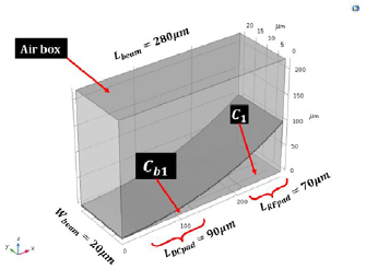
Figure 5. The dimensions considered for the simulation of the switched capacitance element showing mainly the choice of air box dimensions.
Download figure:
Standard image High-resolution image
Figure 6. The COMSOL analysis results for the curvature of the capacitive switched element proposed versus the stress mismatch induced by the plastic deformation of the metal.
Download figure:
Standard image High-resolution imageThe analysis of the clamped-free beam profile in terms of the stress mismatch allows to plot the ratio of the down-state capacitance to the up-state capacitance for the proposed capacitive switch element as demonstrated in figure 7 for both the RF shunting capacitance and the DC actuation capacitance controlling the switching operation itself. The higher the ratio for the RF capacitance, the higher the tuning ratio for the whole 4-bit capacitor based on the element analyzed. Using a similar analysis, the pull-in voltage versus residual stress is plotted as shown in figure 8.

Figure 7. The down-state to up-state capacitance ratio for the RF shunting capacitor of the proposed element and the DC actuation capacitance of the same element versus residual-stress after post-processing.
Download figure:
Standard image High-resolution image
Figure 8. The pull-in voltage for the DC actuation capacitor of the proposed element versus residual stress after post-processing.
Download figure:
Standard image High-resolution imageThe significant difference in the slope for the two curves in figure 7 shows one of the major advantages of the zipper-like switched capacitance element design due to that much improvement of the tuning ratio can be obtained with the increase of mismatch stress at not much increase in the pull-in voltage and without sacrificing the switching time of the proposed element. The COMSOL analysis of the residual stresses in the metal and oxide layers shows that a stress mismatch around 250 MPa leads to about 100 µm tip deflection. Also, the resonant frequency (fundamental mode) is about 18 KHz.
The zipper-like electrostatic actuator allows for lowering the actuation or pull-in voltage of the beam while providing enough mechanical restoring force for the OFF state (up-state). The simulation in COMSOL shows that the mechanical restoring force at the tip of the cantilever in the ON state (down-state) is more than 9 µN. Such mechanical features provide immunity to self-actuation and good power handling capability, especially at relatively low power applications that are the focus of the proposed designs.
In order to achieve such high ratios (see figure 7), e.g. 80 at 250 MPa stress mismatch, the ON-state capacitance across the CPW line should be significantly larger than the OFF-state and the CPW original capacitance which is the capacitance between the ground and the signal line of the CPW. As a design guideline, the overall OFF-state capacitance of the n-bit capacitor should be dominated by the OFF-state capacitance of the capacitive switched capacitor elements. The same guideline is to be employed in the design of the phase shifter. The actual lumped circuit model of the capacitor is displayed in figure 9.

Figure 9. The actual lumped element model of the 4-bit capacitor based on four capacitive switches where the novel approach of electrostatic actuation is demonstrated. The DC bias switches both the RF MEMS capacitor loading line and the coupled actuation capacitor together, thus eliminating the need for resistive or inductive biasing.
Download figure:
Standard image High-resolution imageIn figure 9,  represents the capacitance between the CPW signal pad and the silicon substrate and
  is the resistance through the silicon substrate. The lumped capacitor
  models the capacitance between the signal line and ground of the CPW. For each of the four RF shunt capacitors
  representing the four different bits of the digital capacitor bank, the structure of the capacitive switch elements necessitates the presence of series resistance
  and inductance
  between the RF shunting capacitors and the DC actuation capacitors. The capacitors
  represent the DC actuation capacitors employed for electrostatic actuation of the individual bits using the independent DC voltage controls
 .
.
Referring to the 3D structure of the 4-bit capacitor in figure 2, the DC actuation voltage is applied directly to the metal of the structural layer, which does not impact the RF signal except in the case of collapsing the beam's tip for capacitive shunting. Engaging any of the four bits requires applying the DC voltage to its designated micro-beams such that the voltage difference between the warping beam and the CPW ground plane pulls-in the beam and loads the signal line with significant capacitance, ON-state. As a matter of fact, the coupling of the DC actuation capacitor (that is inherent to electrostatic actuation) and the RF shunting capacitance described earlier makes the equivalent circuit as demonstrated in (b)
Figure 10 A fitting of the finite element method (FEM) simulation results helps calculate the individual values of the lumped elements in this figure.

Figure 10. The effective lumped element circuit model of the 4-bit capacitor; (a) when are beams are up, the OFF state and (b) when all beams are collapsed, on the ON state.
Download figure:
Standard image High-resolution imageFigure 11 displays the HFSS electromagnetic simulation results of the extracted single-port capacitance of the 16 different states of the capacitor. The simulated SRF exceeds 16 GHz whereas the up-state (OFF) capacitance (state 1) is around 50 fF. The footprint of the capacitor is 0.6 mm × 0.9 mm including the 150 µm DC pads. Using the S11 data from the HFSS simulation, the different components in the equivalent lumped element model of the 4-bit capacitor could be extracted in ADS software.

Figure 11. The HFSS simulated capacitance for all the 16 states starting from the first state (all beams up) to the last state (all beams down).
Download figure:
Standard image High-resolution image3. Design and simulation of the 4-bit phase shifter
Figure 12 illustrates the 3D structure of the proposed phase shifter, and an exact layout is displayed in figure 13. It uses a similar architecture of the MEMS capacitive switches for the capacitive loading of the signal line. The actuation voltage found experimentally is up to 70 V depending on the resulting warpage, and comparable values were obtained in COMSOL electromechanical simulations (<65 V). As in the case of the compact 4-bit capacitor, it is possible to use a holding voltage using a bias tee or resistor connected to the signal line. In addition, the symmetric design employed in the phase shifter offers a relatively better matching for no significant deviation in the phase shift performance. If higher resolution of phase shift is required, then the two arrays of beams of the one bit can be actuated one side at a time.

Figure 12. The 3D structure of the compact 4-bit CMOS-MEMS phase shifter.
Download figure:
Standard image High-resolution image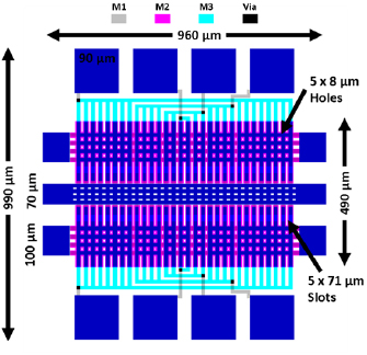
Figure 13. The exact layout of the proposed 4-bit phase shifter showing the main dimensions.
Download figure:
Standard image High-resolution imageAs shown later in the SEM picture of the post-processed phase shifter in section 4, the tip deflection of the capacitive switch elements is around 100 µm. This is the same value that was used in the HFSS electromagnetic simulation shown in figures 14 and 15 for the insertion loss and phase angle, respectively. Among the most important performance parameters for the design of phase shifters is the absolute insertion loss, and insertion loss variation [20, 21]. For different phase values at different states of the device, it is always desirable to maintain the insertion loss at the same value for all states, i.e. to have the smallest possible variation in insertion loss for all states.
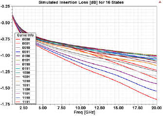
Figure 14. HFSS simulation of the insertion loss for all the 16 states of the phase shifter.
Download figure:
Standard image High-resolution image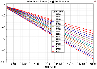
Figure 15. HFSS simulation of the phase variation for all the 16 states of the phase shifter.
Download figure:
Standard image High-resolution imageThe HFSS electromagnetic simulation results in figure 14 show that the maximum insertion loss variation of the phase shifter over the 20 GHz operation bandwidth is around 1 dB, which is relatively good in comparison with the results reported in [19–21]. Additionally, the insertion loss is comparable with bulky MEMS phase shifters designed using conventional surface micromachining fabrication processes. It should be noted that the matching and insertion loss strongly depends on the silicon trench shape and depth. The depth assumed in the HFSS design and simulations is 60 µm.
The simulated phase curve in figure 15 shows that a maximum phase change of 50° is achievable between states 0000 and 1111 at 20 GHz whereas the maximum phase shift at 20 GHz is almost 90°. If the capacitive loading per bit is increased, the phase change can be made considerably larger. The large range of variation is attributed to the thinner thickness of silicon dioxide layers used for the capacitive loading, which takes place mainly in the KOH etch step for finalizing the trench patterning [15, 16]. The simulated return loss of the phase shifter is shown in figure 16.

Figure 16. HFSS simulation of the return loss for all the 16 states of the phase shifter.
Download figure:
Standard image High-resolution imageIt is interesting to note that the device can be used as switchable true time delay line with a fine resolution of 0.5 ps as demonstrated in figure 17.

Figure 17. HFSS simulation of the group delay for all the 16 states of the phase shifter.
Download figure:
Standard image High-resolution image4. Device fabrication and post-processing
Both types of the MEMS devices presented are fabricated using the same post-processing sequence. In this section, an enhanced version of the mask-less CMOS post-processing procedure in [15, 17] is detailed. The expanded version of the post-processing sequence utilizes efficiently the recent advancement in reactive ion etching (RIE) and deep RIE (DRIE) technologies in terms of the cryogenic cooling capabilities of the substrate. The cryogenic cooling allows the control of the substrate temperature under high plasma power. Such high power enables much faster dry etching and as a result a high temperature is induced in the etched films causing warping due to the residual stress. On the other hand, the presence of cryogenic cooling drains the induced heat and allow the control of the residual stresses in the structural layers. Accordingly, it allows varying the warping profile for the same device layout. This fact is employed in this work.
The main post-processing steps are illustrated with the cross-sections in figure 18. The layout for the as-received CMOS chips was designed as shown in figure 18(a). The topmost exposed metal layer (M4) is used as a hard mask for the dry etching of the exposed oxide layers as well as the isotropic etching of the low resistivity silicon in the substrate. In figure 18(b), the dry etching of oxide gives access to the second metal layer (M2) to be later sacrificed for the release of structures made of the third metal layer (M3).

Figure 18. The post-processing sequence employing the enhanced mask-less post-processing of standard CMOS 0.35 µm chips using the cryogenic cooling; (a) the as-received chip with the passivation oxide on top of M4, (b) plasma etching of the oxide stack to uncover the metal and silicon, (c) plasma etching of silicon for the sake of trenching under the RF device, (d) wet etching of the exposed metal layers (M2 and M4) in order to release the MEMS structure, and (e) plasma etching of oxide in order to uncover metal and induce warping.
Download figure:
Standard image High-resolution imageThe subsequent isotropic etching of the exposed silicon layer is illustrated in figure 18(c). It is recommended to perform the wet etching of the sacrificial metal layer M2 and the etching of silicon trench at low temperature. This guarantees no added residual stresses to the metal-oxide structural layers. The cross-section of the device after the wet etching step of M2 and M4 layers, the metal-oxide adhesion layers as well as the silicon pits are shown in figure 18(d). After the proper drying of the wet-released chips in the critical point drier (CPD) using liquid CO2, the third metal layer (M3) is exposed by a second dry etching step of the oxide layer covering it as illustrated in figure 18(e). Uncovering M3 layer allows for probing, wire bonding, and flip-chip bonding.
For wet and isotropic dry etching of large areas, release holes are typically used, but they are not shown in figure 18 for the sake of simplicity. Using an Oxford Instruments DRIE system with cryogenic cooling, the plasma power employed in the C4F8 oxide etching recipe is ~2.5 kW. For small substrates such as the typically few mm CMOS chips utilized in this work, a silicon wafer should be employed as a carrier. The thermal contact required for cooling is ensured via the proper use of commercial vacuum-compatible thermal paste. More than one paste was employed including Cool-Grease (CGR7016) and Fomblin lubricants. The thermal performance was generally very good, however, in terms of efficient cleaning of the backside of the CMOS chips after the plasma etching, pure acetone and isopropyl alcohol were used to clean the thermal paste.
Using the proper residual-stress tuning parameters in the dry etching phase, it is possible to control the stress in the metal-oxide composite beams of the switched capacitor elements such that they warp in the desired orientation as demonstrated in figure 19. The tip deflection shown is close to 100 µm for the 250 µm long capacitive switch elements.

Figure 19. The SEM image of the fabricated 4-bit CMOS-MEMS phase shifter using the proper residual-stress tuning parameters of the cryogenic post-processing sequence; (a) with cryogenic cooling, (b) without cooling.
Download figure:
Standard image High-resolution imageFor the fabricated devices, a significant anticlastic curvature can be observed for large arrays of connected capacitive switches elements. Experimentally, this is found to induce considerable differences between the required actuation voltages of the higher bits (5–10 V). In terms of design and readout circuitry, it is desirable to have the same actuation voltage level for all the bits. The simplest approach to overcome the 2D warpage is to build the different arrays of capacitive switch elements without connecting the elements constituting a given bit. This can increase slightly the actuation voltage required generally, but it would keep the warpage as 1D or longitudinal, i.e. with no anticlastic or transverse warpage.
In terms of capacitance per bit, it is still better to separate the elements representing the different bits in order to be able to maintain the proper scaling of bits, especially between the lowest bits. For instance, in the proposed 4-bit capacitor design, the ratio  is 2.19 instead of 2, the ratio
  is 2.09 instead of 2, and the ratio
  is 2. Another approach is to connect the different elements in an array as implemented for the proposed phase shifters. Disconnecting the tips of the elements helps suppress the anticlastic warpage while connecting the actuation capacitors in order to lower the actuation voltage.
In figure 19, it is worth noting that the as-received residual stresses in the structural layer of the fabricated devices does not result in the desirable warping profile, and tip deflection (figure 19(a)). Using the pulsation technique adopted and proposed in this work, the proper warping profile and tip deflection in the up-state is achievable (figure 19(b)).
Based on the above considerations, the uniformity of tip deflection for the array of switched-capacitor elements constituting a capacitor or phase shifter device is a critical performance parameter. In order to achieve highly uniform as well as repeatable warping profiles for the CMOS-MEMS devices proposed, the presence of cooling at the backside of a given CMOS chip should be, first, reproducible and almost independent of the chip size. Practically, the thickness of the chip helps with that. However, better uniformity of cooling is obtained with the use of proper gluing material as well as thin enough carrier wafer that is used during the release of MEMS devices. For thick carrier wafers, the best approach is to have locally thin areas on the wafer by creating pockets for the chips (such that the thickness of silicon/glass underneath the chips <200 µm). It is worth noting that a silicon carrier wafer is recommended for the sake of providing much more uniform cooling by virtue of the thermal conductivity of silicon.
Another way of suppressing non-uniform deformation of the MEMS structures would be simply in using the same switched-capacitor element such that larger plates are just made of arrays of such relatively narrow element (i.e. narrow beam to prevent anticlastic warpage, which would depend on the width of the MEMS beam/plate). This approach is considered in the paper for the phase shifter mainly.
5. Measurements and discussion
In this section, the measurement results are presented and discussed starting with the results of the 4-bit capacitor then the results of the proposed 4-bit phase shifter.
The 16 different states of the capacitor were all measured, and the extracted capacitance values are plotted in figure 20 over the frequency range from 3–10 GHz. Due to the thinning of the oxide layers during the KOH wet etching step of the silicon trench (in figure 18(d)), the down-state capacitance increases for each switched beam resulting in an overall increase in the capacitance values by more than 10%, with a measured tuning ratio of approximately 10:1. The measured Q for the different states are displayed in figure 21, which is remarkably smaller than the simulated value. This is attributed to insufficient removal of the substrate's low-resistivity silicon that is in the vicinity of the signal line. This includes silicon at the CPW probing.

Figure 20. Measured capacitance values of the 16 different states of the 4-bit capacitor.
Download figure:
Standard image High-resolution image
Figure 21. Measured Q factor including the RF probing pads.
Download figure:
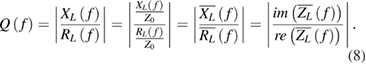
Standard image High-resolution imageThe frequency-dependent quality factor  can be computed for the 1-port capacitor as provided in equation (8).
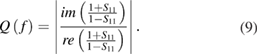
The reflection coefficient at the port is  as shown in equation (9) where the
  is calculated as shown.
In order to investigate the impact of the low-resistivity silicon on the RF performance of the capacitor, figure 22 provides the measured Q values after de-embedding the RF probing pads. In addition, figure 23 demonstrates the measured return loss at the maximum capacitance corresponding to state '1111' versus the extracted return loss using the ADS software package after de-embedding the probing pads.

Figure 22. Measured Q factor after de-embedding the RF probing pads.
Download figure:
Standard image High-resolution image
Figure 23. Measured return loss at the maximum capacitance (state '1111'), S11, versus the extracted return loss after de-embedding the probing pads, S33.
Download figure:
Standard image High-resolution imageIn fact, the lumped circuit element in figure 24 was used after removing the substrate-related circuit elements shown earlier in figure 10. The extracted lumped circuit parameters are summarized in table 1.

Figure 24. The lumped circuit elements of the 4-bit capacitor if the impact of substrate at the CPW port is removed.
Download figure:
Standard image High-resolution imageTable 1. Summary of the lumped circuit element values for the equivalent model of the 4-bit capacitor.
| Lumped element | |||||||
|---|---|---|---|---|---|---|---|
| State# | ![${{C}_{cap}}[{\rm pF}]$](https://content.cld.iop.org/journals/0960-1317/30/4/045006/revision2/jmmab71e6ieqn027.gif) |
![${{R}_{cap}}[\Omega]$](https://content.cld.iop.org/journals/0960-1317/30/4/045006/revision2/jmmab71e6ieqn028.gif) |
![${{L}_{cap}}[{\rm nH}]$](https://content.cld.iop.org/journals/0960-1317/30/4/045006/revision2/jmmab71e6ieqn029.gif) |
![${{C}_{s}}[{\rm pF}]$](https://content.cld.iop.org/journals/0960-1317/30/4/045006/revision2/jmmab71e6ieqn030.gif) |
![${{R}_{s}}[\Omega]$](https://content.cld.iop.org/journals/0960-1317/30/4/045006/revision2/jmmab71e6ieqn031.gif) |
![${{C}_{f}}[{\rm pF}]$](https://content.cld.iop.org/journals/0960-1317/30/4/045006/revision2/jmmab71e6ieqn032.gif) |
![${{L}_{0}}[{\rm nH}]$](https://content.cld.iop.org/journals/0960-1317/30/4/045006/revision2/jmmab71e6ieqn033.gif) |
| 16 | 0.94 | 2.08 | 0.021 | 1.3 | 140 | 0.05 | 0.1 |
| 15 | 0.88 | 2.19 | 0.016 | ||||
| 14 | 0.83 | 2.43 | 0.025 | ||||
| 13 | 0.77 | 2.53 | 0.018 | ||||
| 12 | 0.73 | 3.45 | 0.001 | ||||
| 11 | 0.67 | 3.9 | 0.003 | ||||
| 10 | 0.61 | 3.8 | 0.003 | ||||
| 9 | 0.55 | 4.4 | 0.013 | ||||
| 8 | 0.53 | 4.57 | 0.007 | ||||
| 7 | 0.47 | 4.68 | 0.001 | ||||
| 6 | 0.41 | 6.3 | 0.001 | ||||
| 5 | 0.35 | 7.9 | 0.01 | ||||
| 4 | 0.29 | 4.6 | 0.004 | ||||
| 3 | 0.22 | 6.5 | 0.005 | ||||
| 2 | 0.17 | 9 | 0.004 | ||||
| 1 | 0.1 | 15 | 0.001 | ||||
At this stage, it is instructive to compare the performance of the proposed capacitor to other devices reported. The comparison is provided in table 2. By comparing the proposed capacitor to that in [22], we can see that its size is almost the double. However, it has demonstrated more than twice of the maximum capacitance with more than 40% higher tuning range, higher resonance frequency and of digital type. Digital operation is preferred over analog due to its lower sensitivity towards heat variation and prevents hysteresis [24].
Table 2. A comparison of the performance of the 4-bit compact capacitor to other CMOS-MEMS capacitors in literature.
| Specification | This work | [22] | [23] | [28] |
|---|---|---|---|---|
| Tuning ratio | 10:1 | 6.9:1 | 3.75:1 | 10:1 |
| Max. cap. | 0.94 pF | 0.37 pF | 3.75 pF | ~1 pF |
| Q at 1 GHz | ~100 | 95 | 100 | 160 |
| Self-resonance | ~14 GHz | 11 GHz | ~4 GHz | ~5 GHz |
| Size | 0.54 mm2 | 0.25 mm2 | 3.6 mm2 | N.A. |
| Operation | Digital, 4-bit | Analog | Digital/analog, 4-bit | Digital |
| Actuation | Electrostatic | Thermal + Latching | Electrostatic | Electrostatic |
| Voltage | 50–70 V | 3 V | 60 V | 50 V |
| Op. power | 0 | 15 mW | 0 | <0.5 mW |
It can be deduced that further dry and/or wet etching of the substrate silicon under the probing pads would alleviate the issue with the low Q of the capacitor. Increasing the isotropic etching component in the silicon dry etching process as well as optimizing the design of the release holes would allow better control over the removal of the low-resistivity silicon from underneath the CPW signal line without affecting the structural integrity of the device.
As a matter of fact, the presence of the lossy silicon under the probing pads is essential for its RF testing in terms of on-wafer probing. Generally, the capacitor would typically be part of a larger RF circuit where the use of direct connection to the capacitor is not required. However, it should be noted that wire bonding or flip-chip bonding to the circuit is inevitable, and practical solution to that would be in shielding the CPW as presented in [26–27], where the slow-wave structure is used. It is worth mentioning that the access to etching the lossy silicon in the standard CMOS substrate has been enhanced in the design of the down-to-silicon release holes for the phase shifter as shown in figure 25 where the density of perforations in the CPW signal line and gaps is around 27% whereas the density of perforations is almost 14% for the capacitor.

Figure 25. The SEM demonstration of the silicon substrate etching under the CPW line of the 4-bit phase shifter leading to low insertion loss and showing the improved access to the lossy silicon in terms of the density of release holes.
Download figure:
Standard image High-resolution imageThe impact of the increased density as well as uniformity of release holes can be observed in the measured insertion loss at the different states of the phase shifter, as displayed in figure 26. It is important to keep in mind that the phase shifter is a 2-port device, meaning that an equivalent lumped circuit model like that of the capacitor would include more substrate-related capacitance and resistance elements. This leads to more loss than that affecting the RF performance of the digital capacitor. A manifestation of such loss is given by the insertion loss that is >1 dB at low frequencies in figure 26. The measured results confirm the low variation of the insertion loss that was observed in the simulation results in figure 14. Also, the insertion loss is relatively good. The matching can be examined in the plots of measured return loss displayed in figure 27.

Figure 26. The measured insertion loss for all the 16 states of the phase shifter.
Download figure:
Standard image High-resolution image
Figure 27. The measured return loss for all the 16 states of the phase shifter.
Download figure:
Standard image High-resolution imageFinally, the impact of the shunting capacitance can be examined in figure 28 where the measured phase angle for the 16 different states is plotted. The maximum phase difference measured is around 120° at 20 GHz. Like the 4-bit capacitor bank, part of the insertion loss is due to the lossy silicon in the RF probing pads. In a typical device, there is no need for probing, and the silicon reinforcement at both ports is not needed. The actual device then would be like the one in figure 29. The corresponding insertion loss based on HFSS simulation would then be as shown in figure 30.

Figure 28. Measured results of the phase variation for the 16 different states of the phase shifter.
Download figure:
Standard image High-resolution image
Figure 29. An example of the exact layout of the proposed phase shifter with extra release holes at both CPW ports (with no need for the silicon reinforcement under the probing pads).
Download figure:
Standard image High-resolution image
Figure 30. HFSS simulation of the insertion loss of the proposed CMOS-MEMS phase shifter without the silicon reinforcement under the pads.
Download figure:
Standard image High-resolution image
Another comparison of the performance of the proposed phase shifters to other reported phase shifters is provided in table 3. By comparing to the devices in [12, 25], we can see that the 4-bit phase shifter presented exhibits a significantly higher figure of merit in a smaller area. The insertion loss variation of the device is lower, which is another advantage of the proposed device. At this stage, it should be noted that the phase shifter presented can possibly operate using <50 V actuation voltage. Referring to the design curves in figures 7 and 8, there should be not much trade-off with the overall performance as a result of the reduced tuning ratio.
Table 3. Comparison of the performance of the 4-bit phase shifter to other CMOS-MEMS phase shifters in literature.
| Specification | This work | [12] | [25] | [21] |
|---|---|---|---|---|
Phase shift  |
−150 | ~44 | −128 | ~40 |
| @ 20 GHz | @ 20 GHz | @ 65 GHz | @ 26 GHz | |
| Worst insertion loss (dB) | ~3.0 | ~2.5 | ~4.4 | ~1.0 |
| @ 20 GHz | @ 20 GHz | @ 65 GHz | @ 26.5 GHz | |
| Worst insertion loss rate (dB mm−1) | ~3.75 | ~0.58 | ~3.33 | 0.8 |
| @ 20 GHz | @ 20 GHz | @ 65 GHz | @ 26 GHz | |
| Max. insertion loss variation (dB) | ~1 | >2 | ~2.6 | 0.4 |
| @ 20 GHz | @ 20 GHz | @ 65 GHz | @ 26 GHz | |
Figure of Merit ( |
50 | 17.54 | 29.41 | 40 |
| @ 20 GHz | @ 20 GHz | @ 65 GHz | @ 26 GHz | |
| Worst return loss (dB) | ~7 dB | ~10 dB | ~12 dB | 17 |
| @ 10 GHz | @ 20 GHz | @ 65 GHz | @ 24.5 GHz | |
| Device size | 1.0 mm2 | 2.42 mm2 | 1.04 mm2 | 0.75 mm2 |
| Operation | Digital, 16 states (4-bit) | Analog | Digital, 3 states | Analog |
| Actuation | Electrostatic | Thermal + electrostatic | Electrostatic | Electromagnetic |
| Voltage | <70 V | 48 V | 46 V | 0.1 V |
| Power | 0 | 320 mW | 0 | 5 mW |
At this stage, several design guidelines for the proposed devices can be outlined. Geometrically, any large area that is required for larger capacitive loading of the signal line should be divided in an array of the proposed clamped-free elements of switched-capacitors such that the deflecting beam warps in 1D only, not 2D (depending on the width of the beam. An in-plane beam with an in-plane aspect ratio of 1:10 should be enough analytically for the narrow-beam assumption. Second, in terms of electromechanical performance, it is important to limit the length of the beam in order to reduce the tip deflection at a given stress level (and its corresponding tuning ratio), which would yield a reasonable pull-in voltage (50–70 V). Also, a longer beam means lower actuation/reconfiguration speed.
For the RF design considerations, there are two major concerns. First, it is important to reduce the parasitic capacitances. Otherwise, the resolution in capacitance value would be dominated by the parasitic capacitances, not the elements making the binary capacitor. Second, in order to have good control of the switched capacitor quality factor (Q), it is important to pay attention to the equivalent lumped model to minimize losses in circuit, including losses associated with the CPW pads. The losses of the anchored sections of the CPW should be minimized as they contribute to the overall Q of the switched capacitor.
Moreover, in terms of microfabrication & post-processing, a significantly long beam would tend to be less stiff or weak, which may result in excess warping as well as rupture. Experimentally in-plane aspect ratios of up to 1:20 for the clamped-free beams were found to be safe for all the post-processing steps illustrated in figure 18.
Finally, such MEMS devices are to be packaged for the sake of reliability [1]. As a result, it is important to consider the limitation on the maximum deflection of the clamped-free beams depending on the cavity size of the package. This would trade-off the tuning ratio of the element.
6. Conclusion
This paper has demonstrated the design, fabrication and testing of compact RF MEMS 4-bit capacitors and phase shifters that are implemented in a standard CMOS 0.35 µm technology. The micromachining of both devices is based on the cryogenic-cooling mask-less post-processing procedure allowing warpage control of metal-oxide structural layers. Several design guidelines were outlined in terms of the device's geometry, electromechanical recommendation, RF restrictions as well as post-processing. The approach for the electrostatic actuation employed allowed significant size reduction of both types of designs, with no need for additional biasing circuits while increasing the achieved capacitance density. The measured actuation voltage of the devices is below 70 V.
The digital capacitors demonstrated a maximum tuning ratio close to 10:1 for a capacitance change from 0.15 pF to 1.2 pF with a self-resonance frequency over 10 GHz and a footprint of 0.6 mm × 0.9 mm. The low Q value measured for the compact capacitors is due to the low resistivity silicon in the substrate at the probing locations, which would not be present practically if the proposed devices are integrated in a larger circuit or employ shielding such as slow-wave structures. By eliminating the substrate-related losses, it was demonstrated that the measured Q value would be around 120.
The measurement results of the 4-bit phase shifter confirmed the strong impact of the lossy silicon in the substrate. The measurements of the phase shifters revealed a low insertion loss <3 dB at 20 GHz that is coupled with low variation of the insertion loss <1 dB up to the same frequency. The enhanced access to etching the silicon in the CMOS substrate through the higher density of BEOL perforations contributed considerably to the overall improvement in the loss performance. The overall footprint of the phase shifter is around 1 mm × 1 mm, and the measured maximum phase difference is almost 120° at 20 GHz. The digital phase shifter can also be operated efficiently as a switched true time delay line with a fine resolution of 0.5 ps.