
Abstract
This review focuses on theoretical foundations, experimental implementation and an overview of experimental results of the thermoreflectance spectroscopy as a powerful technique for temperature monitoring and analysis of thermal processes in semiconductor lasers. This is an optical, non-contact, high spatial resolution technique providing high temperature resolution and mapping capabilities. Thermoreflectance is a thermometric technique based on measuring of relative change of reflectivity of the surface of laser facet, which provides thermal images useful in hot spot detection and reliability studies.
In this paper, principles and experimental implementation of the technique as a thermography tool is discussed. Some exemplary applications of TR to various types of lasers are presented, proving that thermoreflectance technique provides new insight into heat management problems in semiconductor lasers and in particular, that it allows studying thermal degradation processes occurring at laser facets.
Additionally, thermal processes and basic mechanisms of degradation of the semiconductor laser are discussed.
Export citation and abstract BibTeX RIS

Original content from this work may be used under the terms of the Creative Commons Attribution 3.0 licence. Any further distribution of this work must maintain attribution to the author(s) and the title of the work, journal citation and DOI.
1. Introduction
From the 1960s, when the history of semiconductor lasers began, performance, efficiency and reliability are the main parameters that influence device applications, common use and development. Heating-induced device failure is a key limiting factor for the device performance and reliability. The problem becomes even more pronounced, when high power devices are considered which, despite high efficiency, are operated at very high driving currents. Therefore, thermal processes in semiconductor laser continue to be extensively studied, as devices become more and more mature.
In order to understand and overcome these problems, an important step is to measure temperature at small size scales with high spatial and temperature resolution. Such information is crucial to optimize thermal design and verify assumptions of numerical simulations.
There are several microscale and nanoscale thermal characterization techniques that could be applied to investigate thermal processes in semiconductor lasers. Each method has strengths, as well as limitations, and generally should be matched to specific experimental conditions: type of device (size, wavelength of emission, operating conditions), required information about temperature of investigated device (spatial, temperature and time resolutions, penetration depth which influence on the area of which we will get the information: facet, whole cavity etc), and specific test requirements. Review of different thermal measurement techniques was presented by Christofferson [1], Kolzer [2], Altet [3] and Cutolo [4]. Such techniques can be distinguished based on their operating mode: contact mode versus non-contact mode. For contact mode temperature measurements, the temperature sensing unit touches the sample. Typical detection approaches include thermocouples, thermistors, and scanning thermal microscopy (SThM) probes [5, 6]. Non-contact (remote) temperature detection is usually preferred for semiconductor lasers, and is accomplished by optical techniques such as thermoreflectance or an infrared imaging. In laser diodes, average active region temperature can be obtained by measuring the emission spectrum of the laser diode and correlating the emission peak shift with heating in the active region [7]. There are also methods of estimation of the internal device temperature, that are based on the drop of the voltage across the device, or decrease of emitted power. In both cases, it is required to register either voltage or power versus temperature for specific operation points. Having this information, it is possible to estimate junction temperature based on the simple measurements.
The non-contact monitoring of the facet temperature is important for investigation of thermal processes and failure mechanisms, and also for increasing reliability and performance of the laser diodes. Three optical, surface-probing thermometric techniques can be used to measure the temperature at the laser diode facets:
1.1. Micro—Raman spectroscopy
Raman spectroscopy examines inelastic photon-phonon scattering processes in a crystal. The scattering of the incident photons by phonons in a crystal leads to shift in energies of the out scattered photons and the creation or annihilation of an optical phonon. The probability of the inelastic scattering is temperature-dependent and is related to the occupation number of optical phonons [8]. Measurement of the crystal lattice temperature is given by the intensity ratio of the Stokes and anti-Stokes lines or by their spectral shift relative to the incident light [9–12]. Temperature resolution of ~5–10 K are given with spatial resolution depending on the excitation laser spot size and can be below 1 µm [13].
1.2. Reflectance modulation (thermoreflectance)
Thermoreflectance spectroscopy detects temperature changes near surface using the dependence of the optical reflectance on temperature. The basic idea is to modulate the sample's temperature and register the changes in reflectivity. Due to its differential nature, modulation reflectance experiment has the potential to suppress broad background features. The resulting spectra exhibit sharp peaks at the energies of critical points (CP) in the band structure. When applied to investigation of devices, the temperature is periodically modulated by injection current, and spectral response is neglected, as only specified wavelength is monitored. The relative change in reflectance upon modulation is very weak on the order of ~10–4 [85, 100]. The spatial resolution depends on the excitation laser spot size. The smallest spot size for 630 nm probe beam wavelength is diffraction limited giving spot diameter of about 0.5 µm. Temperature resolution is better than 1 K [71].
1.3. Photoluminescence spectra measurements
Photoluminescence spectroscopy detects photoluminescence from layers around the QW and waveguide [14–16]. Photoluminescence (PL) occurs when a system makes transition to a higher energy level by absorbing a photon and then spontaneously decays to a lower energy level, emitting a photon in the process. The PL spectra are wavelength and temperature dependent, enabling the determination of temperature fields [17, 18]. While tracing the edge emission, red-shifts of the PL spectrum in a thermally loaded device are interpreted as thermally induced Eg(T) shifts. Using known or separately extracted Eg(T) dependence, facet temperatures are determined. Temperature resolution can be as good as ~1 K and spatial resolution can be as small as 1 µm, being limited by the carrier diffusion length and excitation beam optics [19].
Apart from the surface-probing thermometric techniques, thermal properties of the semiconductor laser were studied by IR imaging [13, 20–24] which provides fast information about temperature profiles and hot spot location, and wavelength tuning technique [25] which is used to determine the time resolved bulk temperature. These two techniques give information about bulk temperature, what is not a case for surface probing techniques.
In this review, application of thermoreflectance spectroscopy for analysis of thermal processes in semiconductor lasers is considered. Thermoreflectance, through high sensitivity and high spatial resolution, is capable of sensing temperature variation due to both operation of devices (in the case of diode laser: Joule heating, and absorption of laser radiation) and local surface or subsurface defects at micrometer and even sub-micrometer scale.
Experimental results of thermal characterization of different types of lasers are presented. The work is organized in the following way: Thermal processes in semiconductor lasers and basic degradation mechanisms are given in section 2. Section III presents theoretical foundations of thermoreflectance spectroscopy. Section 4 concerns experimental implementation of thermoreflectance technique to study semiconductor lasers. Section 5 summarizes experimental results of analysis of thermal processes in semiconductor lasers: high power semiconductor lasers, high power laser bars, quantum cascade lasers (QCL), Vertical External Cavity Emitting Lasers (VECSELs) and GaN-based lasers.
2. Thermal processes in semiconductor lasers. Basic degradation mechanisms
Studies of degradation mechanisms in the GaAs based devices have been performed from mid 1960s [26–28] beginning with those concerning GaAs homojunction laser diodes. After the development of heterostructure lasers and the achievement of CW operation at room temperature (early 1970s), problem of degradation of lasers became apparent. In 1973, Deloach et al, found that the rapid degradation is associated with 〈1 0 0〉 dark line defect growth in the active layer [29]. Petroff and Hartman, clarified that the elongation of the dislocation network, originating from a threading dislocation is the cause of the rapid degradation [30]. In 1974, Ladany and Kressel, reported that facet degradation is a serious problem in laser [31]. They also reported that facet coating was effective in suppression of facet degradation in 1978 [32]. In 1978, Yuasa et al, verified that the facet degradation is due to photo-assisted facet oxidation [33].
Reliability of semiconductor devices has been greatly improving for about 40 years since CW lasing at room temperature was achieved in AlGaAs/GaAs laser. Throughout this period, various degradation mechanisms were discovered and reliability improved, allowing to extend lifetimes from only a few 100 h to several hundred thousand hours.
Short overview of semiconductor laser diode degradation mechanism is presented below. The degradation modes can be classified in terms of time evolution of laser parameters under laser operation. Normally, degradation is measured as the evolution observed on either the light output power at constant-injection-current operation or the threshold current at constant light output power. The latter test is usually preferred because, for example, lasers for telecommunications work at constant light output power. Although apparently similar, both modes are not equivalent; in fact, the constant-output power mode implies a progressive increase in the injection current as device performance degrades. This increasing injection current increases the temperature of the junction, the opposite of what happens in constant-current mode [34]. Phenomenological classification of degradation modes [35–38]: gradual degradation, rapid degradation and sudden degradation also called catastrophic degradation is as follows:
- Rapid degradation normally is observed in the first 100 h of operation. It appears as a quick decrease of the optical output power or a quick increase in the threshold current. This failure mode indicates significant defects, e.g. cracks or large dislocation networks, already present after device manufacturing [36].
- Gradual degradation is a very slow process that extends over several thousands of hours and manifests itself as a slow output power decrease (slow threshold current increase), resulting a gradual decrease of the quantum efficiency. This is a characteristic behavior for regular operation. It includes point defect creation and defect motion through the material, both on long time scales [36].
- Catastrophic degradation is a very fast process that appears suddenly after a regular operation life of a laser. This kind of degradation gets activated when a threshold condition is reached, that triggers the start of a fast degradation process. This degradation mode appears suddenly without a previous signature that such a failure could occur. Therefore, it is very difficult to screen. The origin for catastrophic degradation may lie inside the device or at the facets. The most important case in state-of-the-art devices is due to damage starting at the outcoupling facet, called catastrophic optical (mirror) damage (COD). Usually this mode limits the maximal output power of a laser device and, consequently, is observed predominantly at high injection currents. The term catastrophic degradation refers to catastrophic damage to the inner cavity, whereas COD specifically refers to catastrophic damage to the mirror facets. This degradation mode is also referred as catastrophic optical mirror damage (COMD) in the literature [39].
Since mirrors are of critical importance for laser diode reliability, the phenomena of COD should be discussed briefly. While the lifetime of low-power laser diodes is limited by gradual degradation, the maximum optical power of high power laser diodes is mostly limited by the COD. This degradation mode has received a great deal of study. Shortly after the first realization of the diode laser, reports were published addressing the observation of COD by Cooper et al [27] in 1966 and Kressel et al [40] in 1967. In 1973 Eliseev [41] characterized it as thermal micro-explosion. Henry et al have published a comprehensive work, also addressing the origins of COD and its kinetics, in 1979 [42]. The main findings of this study are still valid for recent DLs: COD is jump-started by a fast-thermal runaway. This process is initialized if a certain temperature at the later COD site is achieved, named critical temperature (Tcrit). Direct experimental verification of such process has been reported for the first time by Tang et al [10]. In later studies [43–47], the influence of extrinsic effects was shown such as surface recombination and creation of structural defects [48]. The mechanism leading to COD can be described by the following sequential steps: nonradiative recombination at the mirror facet increases the local temperature with concurrent band-gap shrinking, which increases the light self-absorption at the facets, generating additional e-h pairs, which recombine nonradiatively, further increasing the temperature of the facet region. Nowadays, problems of mechanisms and kinetics of the catastrophic optical damage of diode laser are still extensively studied [36].
The precondition for COD is an elevated local temperature. This can be caused by different heating mechanisms. At the facets, the dominating ones are surface recombination [49] and surface currents [10]. The main heat source is the nonradiative carrier recombination, which releases thermal energy to the lattice. Therefore, the intense local heat generation is associated with a high nonradiative recombination efficiency, which can result from different causes:
- High concentration of nonradiative recombination centers, usually related to the quality of the facet region in terms of defects, stoichiometry, impurities, and oxidation;
- High surface recombination velocity (SRV), which depends on the material forming the active region of the laser and the surface conditions
- High concentration of free carriers, which can recombine, releasing thermal energy.
At low laser power, the main source of free carriers is carrier diffusion from the inner part of the laser, whereas at high laser power, the main carrier generation mechanism is the strong photo-generation by laser light self-absorption owing to thermally induced shrinkage of the band gap at the facet region. Inspection of the laser after degradation enables to establish degradation classification based on the part of the structure that was damaged. Two degradation modes are distinguished: internal and external degradation.
Internal degradation usually is found in the active region. Generally, it can be related to crystal-defect reactions (e.g. diffusion, generation and motion of defects) that occur during the laser operation. This type of degradation is closely related to the properties of the materials and interfaces forming the chip. Internal degradation is accelerated by strain, temperature, injection current and light power.
External degradation can occur in different parts of the device:
- Mirror facet. Mirror facets are critical for laser degradation. The COD mechanism mentioned previously is related to a sudden failure of the device associated with local melting at the facet.
- Electrodes. The electrodes usually degrade by metal electromigration inside the chip. This phenomenon is enhanced by current injection and temperature. The main factor contributing to temperature increase at the electrode is Joule heating.
- Heatsink bonding. The chip is bonded to a heatsink in order to dissipate the heat generated by laser operation. This bonding is achieved by soldering with a metal. Bonding degradation is related to the properties of the metal solder; in particular metal migration appears among the causes for this degradation. Also void are formed and contribute the degradation. Metal migration is induced by current injection and ambient temperature. Temperature increases mainly by Joule heating.
- Metal coating the heatsink. The enhancement factors are the same as those reported for metal bonding. The main problem concerns the adherence of the metal to the heatsink.
As it was described earlier, the heat is one of the main enhancement factors of degradation of particular parts of the laser. Scheme of interconnections between process in semiconductor laser, which can lead to gradual and catastrophic degradation is presented in figure 1. It can be observed, that increase of the temperature in the active region and at the facet of semiconductor laser is the main factor, which enhances degradation processes. The main stream of energy is given in the upper row; it consists of an energy conversion chain from the input electrical energy to electronic energy (of electron-hole pairs in the active region), then to optical energy (the photons accumulated in the cavity) and then to output laser emission. Dissipation mechanisms are the base of degradation processes, and they are Joule losses, nonradiative recombination losses and reabsorption of photons (the latter is of non-dissipative nature except for this part which contributes to nonradiative recombonation). Intermediate factors are temperature of the active region (over the whole active region), current redistribution (especially the temperature-induced part), temperature rise at the surface and thermal band gap shrinkage. When the temperature reaches a critical value for surface destruction (melting, as a particular case), the irreversible damage can occur immediately. The temperature rise (both in the whole active region and at the surface) contributes to the acceleration of gradual surface degradation, which includes oxidation, erosion, defect formation and migration inward. There is a feedback from the gradual surface degradation to the total nonradiative recombination; therefore, the process leading to damage would be favored. This is a basic cause of sudden failure during operation time. There are other feedback loops such as the temperature rise at surface, leading to thermal bandgap shrinkage, photon reabsorption and nonradiative recombination. This one supplies the optically induced thermal runaway with a probable damage in the end. Another is the temperature rise at the surface leading to current redistribution and nonradiative recombination. This is a path for current-induced damage, which can be mixed with optical damage or act separately [39].
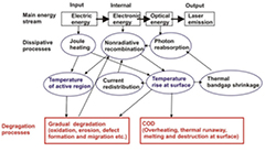
Figure 1. Scheme of interconnections between process in semiconductor laser which can lead to gradual and catastrophic degradation after Eliseev. Reprinted from [39], Copyright 1996, with permission from Elsevier.
Download figure:
Standard image High-resolution imageThis scheme confirms that knowledge about temperature (in particular temperature distribution) during operation of devices is crucial to achieve reliable device operation. Understanding thermal processes, thermal properties and degradation mechanisms in devices is also important for optimization of semiconductor lasers.
3. Basics foundations of thermoreflectance spectroscopy
Modulation spectroscopy started in 1960s [50] and proved to be a very powerful and versatile optical experimental technique for studying the properties of bulk semiconductors, micro- and nanostructures (quantum wells, superlattices, quantum dots), as well as the characterization of actual device structures (transistors, semiconductor lasers, HEMTs) and verification of growth and processing of devices.
In the first decade, these techniques were applied to characterization of bulk materials and were developed mainly by Cardona [51], Pollak [52], Aspnes [53], Hamakawa and Nishino [54]. In the 1980s, modulation spectroscopy enjoyed a renaissance. It turned out that the same advantages which were exploited for bulk studies were also evident in the semiconductor microstructures fabricated by modern thin film technologies, such as molecular beam epitaxy (MBE) or metalorganic chemical vapour deposition (MOCVD). Modulation spectroscopy deals with the measurement and interpretation of changes in the optical response of a sample which are caused by modifying in some way the measurement conditions. This can easily be accomplished by periodically modulating some parameter applied to the sample, such as an electric field (electromodulation spectroscopy including contact and contractless modes), temperature (thermomodulation spectroscopy) and stress (piezomodulation spectroscopy). This kind of modulation spectroscopy belongs to 'external' modulation [55–60]. The change can also occur if we periodically modulate the wavelength [61] or polarization condition [62, 63]. This kind of modulation spectroscopy is referred to as 'internal' modulation. In other words,
Modulation spectroscopy measures the change of the complex dielectric function

induced by some periodic perturbation.
 and
and  are the real and imaginary parts of the dielectric function, respectively. The relation between the
  and
and  is called the Kramers–Kronig relations and is the following:

where  means the principal value of the integral
In general, the change induced by modulation can be observed either in transmission or in reflectivity measurements. When changes in reflectance spectrum caused by external periodical perturbation are observed we have reflectance modulation spectroscopy.
The relationship between the reflectance modulation and corresponding modulation of dielectric function is complex/quite involved. However, it can be presented with the introduction of so-called Seraphine coefficients  and
and  :
:
where

and


In general,  (refractive index) and
  (extinction coefficient) are the real and imaginary part of complex refractive index
  and can be expressed through the real and imaginary parts of dielectric function, as:
The complex refractive index is related to dielectric function  by:
by:


The reflectivity R of the material for normal incidence of light is given by relation:
In the reflectance modulation, the relative change in reflectivity  is estimated, yielding:
where  and
and  are the changes in n i
  resulting from the modulation.
The modulation spectroscopy is an analogue method for taking derivative of the optical spectrum (reflectance or transmittance) of a material by modifying in some manner the measurement conditions. The observed normalized changes are usually small so that the difference signals are closely related to a derivative of the absolute spectrum with respect to the modifying parameter. The derivative nature of modulation spectroscopy emphasizes structure localized in the energy range of interband (intersubband) transitions of semiconductors (microstructures) and suppresses uninteresting background. The weak features, which might not be seen in the absolute (initial) spectra are enhanced. Therefore, a large number of easy-to distinguish sharp spectral features can be registered even at room temperature. The power of modulation spectroscopy is illustrated in figure 2.
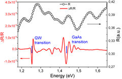
Figure 2. Reflectance and photoreflectance spectra of GaAs measured at 300 K (ITE unpublished result).
Download figure:
Standard image High-resolution imageFigure 2 shows a comparison of the experimental reflectivity (R) and electric-field modulated reflectivity (electroreflectance: ER) spectra of AlGaAs/GaAs laser structure measured at 300 K. Notice that the reflectivity is characterized by broad features, while the modulated (ER) spectrum is dominated by a series of very sharp, derivative-like features, corresponding to transitions in CP.
Thermoreflectance spectroscopy is a one of modulation techniques relying on measuring the change of reflectance spectrum caused by periodic variation of the temperature of the sample. The temperature modulation in thermoreflectance results in the change of dielectric function, which is induced by the shift of the bandgap energy  and by the change of the broadening parameter
  [64].
[64].
Detailed derivation of the expressions of  as well as
  can be found in [65].
4. Experimental implementation of thermoreflectance technique to study semiconductor lasers
This section provides information about implementation of the thermoreflectance spectroscopy technique to analysis of thermal processes in semiconductor lasers.
4.1. Thermoreflectance in analysis of devices and materials
Thermoreflectance spectroscopy has been used to study band structure and dielectric function of semiconductors. Batz was the first to report the thermoreflectance spectrum of germanium in the photon energy region below 5 eV over a wide temperature range [66, 67] and compare experimental results with calculated TR spectra [68]. In 1968, Matatagui presented thermoreflectance spectra of GaAs, GaSb and other semiconductor compounds measured at 80 K and 300 K [65].
Analysis of thermal processes of semiconductor laser by means of thermoreflectance spectroscopy was initiated by Epperlein in 1990s [69–71]. This was the first demonstration of using TR as thermometer, neglecting the spectral information brought by the TR spectroscopy. Instead of registration of the full, energy resolved spectra, Epperlein has analyzed changes in signal registered for specified wavelength. Epperlein studied the impact of temperature on the failure of semiconductor lasers. In papers [70, 71] he reports that this technique enables additionally mapping of the temperature distribution on the front facet laser mirror.
In 1994, Mansanares et al [72] presented work about determination of the temperature distribution in InP/InGaAsP laser diodes using photothermal reflectance microscopy. They demonstrated the weak temperature dependence on nonradiative recombination at the laser facet. In 1998 Dacal et al presented work on heat source distribution and coating influence on temperature distribution in 980 nm emitting laser diodes [73].
As the imaging thermometric technique, thermoreflectance can be used in the two configurations: point-based laser scanning method and with multi-point detection system (CCD TR [74–76]. In-depth description of CCD-TR, its principles and applications are presented in the review paper [77]. CCD TR offers advantages over standard TR in terms of speed of image acquisition. It proved to be suitable to investigation of devices such as resistors, transistors, or electrical interconnects in microelectronics. In 2000s, Grauby et al [75], presented first paper about using a photothermal microscope, presenting thermal image of an electronic component working at a 'high frequency' using a charge coupled device (CCD) camera and a multichannel lock-in scheme. Christofferson et al [74], presented a visible light thermoreflectance imaging with 34 mK sensitivity in order to analyze in real time thermal images. CCD-TR was applied to investigate temperature in semiconductor lasers: high-power laser diodes, quantum dot lasers and VCSELs, all emitting wavelength above 1 µm, avoiding problem of registration of emitted radiation (near field) superimposed on temperature data. In 2014, Raad et al [78], demonstrated the work about capability of using an optically-based measurement system to map the temperature field at the deep submicron level of devices that emit strong light, such as high-power lasers by using filters indiscriminately can reduce the useful signal and render an optical approach unusable.
CCD-based TR was used to image heat transfer in 1.5 µm, high power, large mode emitting laser [79]. Resulting temperature maps and profiles were used as inputs to finite element based optical mode solver.
Using CCD-TR, quantum dot lasers [80] were characterized. Resulting high resolution temperature profiles, allowed to identify separate heat sources due to contact heating and non-radiative recombination in active region.
CCD-TR was applied to study VCSELs [81–83] resulting in top surface 2D temperature maps. Temperature profile was found to have parabolic radial variation, with maximal heating in the centre of VCSEL. The CCD TR was also successfully employed in characterization of QCLs [84].
In 2016, Kim et al [85], register thermoreflectance spectra, reflection and thermoreflectance images of the multi-layered semiconductor devices (polycrystalline silicon micro-resistor on a SiO2 layer/Si substrate using spectroscopic thermoreflectance microscopy based on the CCD camera.
Thermoreflectance spectroscopy was also successfully implemented as a powerful and non-destructive optical technique for investigation of both temperature distribution and heat propagation in devices such as: microelectronic devices [86]: transistors [87–90] interconnects [91], and solar cells [92].
In 1996, Abid et al [93], captured temperature distributions in large-area power transistors. The thermoreflectance technique has also been applied for the extraction of thermal properties of thin films. Thermal transport in metal films was investigated (Clemens et al, in 1988, Miklos and Lörincz in 1989) by monitoring the shape of the temperature decay after termination of a short-duration heating laser pulse [94, 95]. Thermoreflectance was employed in pump–probe configuration to study phonon transport and the thermal relaxation of carriers on picosecond time scales [94]. Transient thermoreflectance [96] and photomodulated thermoreflectance [93] have been used to characterize thermal diffusivity and other thermal properties of thin films.
4.2. Experimental implementation of TR to semiconductor lasers
The main idea of the thermoreflectance spectroscopy relies on measuring of relative changes of reflectivity of the sample induced by periodic variation of temperature. The sample's temperature can be changed in many ways. It can be direct heating, electrical heating (Joule heating) or optical heating with the laser pulse.
In case of thermoreflectance measurements of the laser diode facet temperature, periodic temperature modulation was induced by operating the device in pulse mode. The probe laser beam incidents perpendicularly to the facet and is reflected back. The periodic temperature change of the laser induces variations of the refractive index and consequently modulates the probe beam reflectivity.
The experimentally registered relative reflectance change ( ) is connected with change of temperature (
 ) by the equation reported by Epperlein:
Relative change in the optical reflectance per unit temperature change is termed the thermoreflectance coefficient (CTR). TR coefficient depends on probed material [65], on the specific details of the experimental set-up (numerical aperture of the microscope objective etc [97]. and most importantly, on the wavelength of probe light [98]. Therefore, it should be determined experimentally for each investigated device type and material. The thermoreflectance coefficient its typical magnitudes range from 10−6 to 10−4 for metals and semiconductors [65].
4.3. Thermoreflectance experimental set-up
Thermoreflectance measurements can be realized in two experimental setups: namely charge-coupled device (CCD) camera set-up (CCD-TR) [75, 98, 99], in which a lamp is used to produce the probe light and the whole thermal image is stored in a snapshot, and the focused laser beam set-up (scanning probe TR) [70, 90], which uses the laser line as probe beam and stores the thermal image by scanning the sample surface.
Scheme of focused beam TR experimental set-up used in the experiments is shown in figure 3. Different sources of probe beam can be used, according to specific requirements of studied device, e.g.: Ar+ laser lines (457.9, 476.5, 488.0, 496.5, 501.7 and 514 nm), HeNe laser line 632.8 nm, or UV diode pumped solid state laser (DPSSL) 355 nm.

Figure 3. Experimental set-up for thermoreflectance mapping of laser and laser bar mirrors. Reproduced from [151]. CC BY 4.0.
Download figure:
Standard image High-resolution imageThe optimal wavelength of the laser line used as the probe beam has to be determined by optimization procedure. An appropriate choice of the probe wavelength is very important because it maximizes the thermoreflectance signal, which are of the order of 10−4 to 10−6 [100]. Other authors report ΔR/R change in the range of 10−3 to 10−5 [85]. Optimal probe beam wavelength strongly enhances the sensitivity of the technique to small temperature changes. Procedures of calibration will be discussed in section 4.4.
The probe beam enters a commercial microscope and is focused on the sample surface to a spot diameter about  , when using a 0.65 numerical aperture 74 × objective. The typical probe beam power on the sample surface is 100 µW. It can be assumed, that such low power probe beam does not introduce additional heating of the sample [65]. The probe spot and the laser facet are simultaneously visualized by a CCD camera. The reflected beam is directed onto a Si photodiode detector and the resulting output is fed into a lock-in amplifier. An output signal from the Si detector is lock-in analyzed. A lock-in detection technique is helpful to reach a sufficient signal to noise ratio. The signal
  is normalized by a simultaneously measured dc
  component resulting in information on the relative reflectance change (TR signal). The technique has a spatial resolution of about ~1 µm and temperature resolution better than 1 K. Epperlein reported a value of 0.5 K [71]. It is very important to stress that after reflection, the probe laser beam and laser radiation go along the same path (with the same phase as TR signal) and it is very important to cut off/block the laser radiation from the TR signal and detection. It can be done by application use of appropriate cut-off filters.
The additional chopping frequency allows for simultaneous measurement of reflectivity of the samples. It enables to obtain in the same experiment the value of the reflectivity change  and the reflectivity R in each point of examined area. By dividing
  by R we can eliminate features originating from mechanical roughness of the surface and other artefacts which have nothing to do with actual temperature change. Another method that provides the experimental value of normalized reflectivity (
 /R) is to divide the ac output signal from the Si photodetector by its dc component, which results in:

This method results from the fact that thermoreflectance signal consist of dc part-Sdc and a small ac component Sac resulting from the change  in the reflectivity of the sample, caused by the temperature modification
  [101].
The main part of the experimental set-up is based on an optical microscope, which provides proper mechanical stability and optimal beam alignment.
During the measurement, the semiconductor laser was mounted on a temperature-stabilized heat sink with a water-cooled Peltier element. The whole assembly was mounted on a x-y-z piezotranslator stage which provide 300 µm travel distance and allows precise mapping of the whole facet area with a 0.1 µm step. The device is usually driven with variable frequency pulsed current (up to single kHz range) with variable duty cycle. Under these conditions the laser is operating in quasi-cw (quasi-continuous wave) mode and is subjected to the thermal effects associated with CW operation. The modulated current applied to the sample is supplied by a laser diode driver by function generator.
The main limitations of the technique stem from several factors. One of them is thermal time constant of the system under study. For diode lasers, the thermal time constant is on the order of microseconds. However, applying too high frequency of repetition of pulses, results in minimization of temperature modulation caused by heat accumulation effects. This effect is experimentally observed as reduction of registered temperature increase despite increase of the supply current, or the increase of the duty cycle.
The other factor influencing the technique is the signal-to noise ratio. This in particular limits short pulse regime. For too short pulse lengths, the TR signal can be too weak to become apparent. In other words, the signal might be obscured by the noise. Therefore, although we have been able to register thermal data for measurements for pulses as short as 200 ns, application of relatively high current to the sample was required.
4.4. Temperature calibration techniques
Thermoreflectance, requires calibration procedures, similarly to any other thermometric technique. This is of particular importance for the TR studies of semiconductor lasers, which constituent materials have optical properties that are not well characterized or can vary depending on the growth and processing details. Few data exist for the absolute values of TR coefficient CTR in the literature. Due to the fact that the coefficient CTR depends both on probed material, and the experimental conditions, it should not be taken from the literature, but rather determined in situ, on the probed material itself.
TR spectra shown in figure 4 show why optimization of probe beam wavelength and calibration are important for TR measurements. More details can be found in [102]. Figure 4 presents experimental TR spectra for two materials, namely GaAs and AlGaAs (45% Al content), which are typical materials of near-IR (808 and 980 nm) emitting laser diodes.
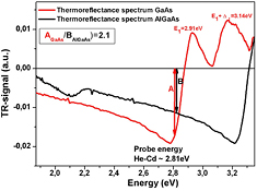
Figure 4. Thermoreflectance spectra for GaAs (red line) and Al0.45Ga0.55As (black line) at 300 K. Reproduced with permission from [108].
Download figure:
Standard image High-resolution imageIf He–Cd laser line (2.81 eV) is used as probe beam in experiments, registered TR signal connected with GaAs is 4 times higher than in case of He–Ne laser probe beam (energy 1.95 eV). Therefore, TR signal value for different materials in the diode laser chip varies with probe beam wavelength used in the experiment. This effect has direct influence on the experimental results. Figure 5 presents exemplary TR signal map where the discontinuity in the intensity of TR signal is clearly visible.
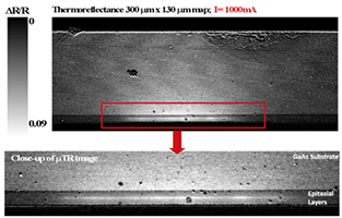
Figure 5. Thermoreflectance 300 × 130 µm map of the facet of HP LD register for supply current of 1000 mA. (ITE unpublished result).
Download figure:
Standard image High-resolution imageThis intensity change is related to different mirror material and consequently different value of thermoreflectance coefficient, and does not reflect rapid change (decrease) of temperature. The darker stripe at the bottom of the picture corresponds to the waveguide region consisting mainly of AlGaAs (7 µm thick). The upper part of the map (brighter) corresponds to pure GaAs substrate material. In order to remove the discontinuity in the intensity of the TR signal, it needs to be recalculated using proper thermoreflectance calibration coefficients CTR for each material in the examined area.
The most obvious way to perform this calibration is to use a second thermometer, for instance a thermocouple thermometer. However, in case of semiconductor lasers this direct calibration procedure is not practical, because of the poor spatial resolution of the thermocouple (compared to size of region of interest—active region of a diode laser), as well as the fact that contactless measurement is required.
Calibration performed in the TR setup (in situ) is preferred, as it does not require additional experimental setups to be analyze the TR data. There are two in situ calibrations that have to be considered. One, is the optimization of the probe beam wavelength. The other is finding the value of the CTR coefficient at given probe wavelength. Both allow recalculating the TR signal into temperature. They both have significant impact on results. An optimization procedure results in both the optimal wavelength (increased sensitivity) as well as the value of the CTR. This method is preferred in case of device based on new material system being studied, when the TR spectrum is not known. This optimization should be performed for each type of examined structure before actual thermoreflectance measurements. On the other hand, it is frequently required to determine the CTR coefficient for a given device, at given probe beam wavelength.
In order to maximize the TR signal, a procedure of determining the proper probe beam wavelength is performed. It relies on measurement of the change of the reflectance spectra with temperature as a function of the wavelength  . The reflectance spectra for various temperatures T are acquired and
  is calculated numerically. To guarantee sufficient accuracy, the temperature of the sample needs to be stabilized and measured precisely, close to the laser chip. The precise temperature control of the device is performed by a temperature controller and a water cooled thermoelectric element. The resulting, exemplary spectrum of
  measured on semiconductor laser bar mirror is presented in figure 6.
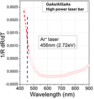
Figure 6. Thermoreflectance sensitivity spectrum  measured on GaAs-based high power laser bar mirror. Reprinted from [111], Copyright 2009, with permission from Elsevier.
Download figure:
Standard image High-resolution imageThis thermoreflectance sensitivity spectrum shown in figure 6 was measured on the GaAs-based high power laser bar structure. A maximum TR signal was obtained in the range 400 nm–900 nm. In the remaining spectral region, the TR signal is substantially lower. The optimal wavelength for examined structure (i.e. the wavelength for which the response to temperature change is the highest) is about 440 nm. For practical reasons 442 nm (2.81 eV) line of He–Cd laser was used as probe beam source for measurement of this device.
This calibration method results in the numerically determined TR spectrum, giving the CTR values versus wavelength. However, it would not be very practical to extract values of CTR for different material layers composing the semiconductor laser. Therefore, having once determined the optimal wavelength for material system under study, it is necessary to determine CTR values for the different materials of the device, according to the equation, which links the relative changes of reflectance with the change of temperature:
This procedure was described in detail in work [103]. In general, this procedure is performed for the non-operating device, heated by an external heat source (thermo-electric controller (TEC), operating in the heating mode). At each temperature setting a reflectance line-scan starting at the substrate and going towards the edge of the p-type contact is registered. This way, the different reflectances of the materials involved into the laser structure could be taken into account by the calibration procedure. Figure 7 shows the dependence of the reflectance signal R on the temperature at two spatial positions of the laser facet, namely at the GaAs substrate and at the epitaxial layers. From a linear fit of the data the  is calculated. The thermoreflectance coefficients obtained by this procedure are CTR-Het = 8.63 × 10³ K (average value for epitaxial layers) and CTR-GaAs = 3.45 × 10³ K (GaAs substrate).
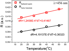
Figure 7. The dependence of the reflectance R on the temperature for the GaAs substrate and for the heterostructure area. [103] 2008 © Springer Science+Business Media, LLC 2008. With permission of Springer.
Download figure:
Standard image High-resolution imageThe calibration, serving as well as confirmation of the correctness of TR results, can also be done by micro-Raman measurements [12, 102] and micro-photoluminescence (PL) [104].
5. Review of experimental results
In this chapter results of the analysis of thermal properties and degradation behavior of semiconductor laser diode will be presented.
5.1. High power semiconductor lasers
High-power diode lasers (HPSL) have become the key element of a laser systems which compete with or replace gas lasers and lamp-pumped solid state lasers. High power diode lasers continuously enter the industrial market as they are compact, easy to cool, yield power efficiency beyond 50% (i.e. about five times higher than any other kind of laser can offer) and their cost is at commonly acceptable level.
As the demand for high optical power continues, the power density at the laser mirror increases. Therefore facet-temperature measurements under high power operation is crucial, providing insight into heat generation and failure mechanisms of high power lasers.
In this section, we present the results of facet temperature measurements of HPSL obtained using thermoreflectance spectroscopy.
5.1.1. Analysis of different mounting arrangements and assessment of different etching technologies on the laser mirror temperature.
TR experiment has been used to assess the influence of mounting arrangement on the observed facet temperatures of laser chips. Two types of InGaAs/GaAs lasers emitting at λ = 980 nm were investigated: mounted epi-layers down on SiC heatspreader and copper HS, as well as epi-layers up. The series of temperature distribution maps for increasing value of driving current for laser mounted epi-down onto SiC is shown in figure 8(b) together with SEM photograph and scheme of epitaxial layers (figure 8(a)) [105].
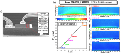
Figure 8. (a) SEM photograph with scheme of epitaxial layers of the high power laser. (b) Temperature distribution maps for high power laser mounted epi_down for different driving currents. The CW optical power emitted for each supply current equals: 50, 250, 450, 650, 1300 mW. Reprinted from [105], Copyright 2006, with permission from Elsevier.
Download figure:
Standard image High-resolution imageWe observed, that heat is generated mainly in the active area and is effectively extracted to the heat sink. Facet temperature at active region is in low teens, even for currents well above 1 A.
Facet temperature increases in active area of epi_down mounted HPSL are compared with results epi-up mounted device. Figure 9 shows comparison of maximum temperature increases in the active region for both investigated devices.
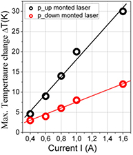
Figure 9. Maximum temperatures increase in the active region for high power semiconductor laser mounted respectively: epi_up (black circle) and epi_down (red circle). (ITE unpublished result).
Download figure:
Standard image High-resolution imageThe maximum temperatures increases are higher (especially for higher driving current) for epi_up mounted devices. This fact is well explained by numerical simulations, showing that mounting has significant influence on the efficiency of heat extraction. Less efficient heat extraction occurs in the case of epi-side up mounting, as the generated heat has to be extracted mainly through thick substrate of relatively low thermal conductivity [105].
As the facet temperature is expected to depend on the non-radiative surface recombination of carriers, the assessment of different mirror etching technologies was performed using TR measurements.
The temperature distribution maps register for cleaved, oxygen plasma RIE-etched and CIBE-etched laser mirror do not show any excessive damage to the mirror surface, produced by etching. The maximum temperature increases above the ambient temperature at the facet are slightly higher for oxygen plasma-treated surfaces (about 20 K for 600 mA), comparing to 15 K for CIBE-etched surfaces. This is 1.5–2 times higher than for cleaved surfaces (figure 10). Results prove that mirror etching techniques used to fabricate unstable resonator potentially result in increased mirror temperatures. This leads to decreased reliability and lifetime of device as it is more prone to optical mirror damage due to higher surface recombination rates [105].
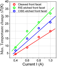
Figure 10. Maximum temperatures increase in the active region for high power semiconductor lasers with different mirror treatments. (ITE unpublished result).
Download figure:
Standard image High-resolution image5.1.2. Facet heating mechanisms in high power semiconductor lasers.
The following study reports on mechanisms of facet heating in HPSL by comparing the facet temperature distributions for fresh (undamaged) and degraded laser. Investigated laser diodes were the broad-area devices based on double-barrier separate confinement heterostructure (DBSCH SQW) designed for 808 nm emission wavelength, grown by MOCVD [106]. Figure 11 shows Al content and (Zn, Si) doping profiles (black solid and dotted lines, respectively) for (DBSCH SQW) structure together with calculated optical field intensity TM0 profile (I-gray solid line).
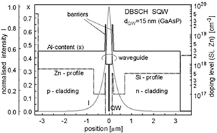
Figure 11. The scheme of DBSCH SQW laser. Reproduced with permission from [108].
Download figure:
Standard image High-resolution imageThe DBSCH design was used to reduce the vertical beam divergence and to increase the COMD level of these high-power laser diodes [65]. Temperature distribution maps for high power lasers were measured using as a probe beam the 442 nm (2, 81 eV) line of the HeCd laser [107]. Temperature distribution map and temperature line-scans across the facet at different driving currents are presented in figure 12.
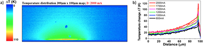
Figure 12. (a)Temperature distribution map for 2000 mA supply current and (b) temperature line scans taken at the center of the active area perpendicular to the epitaxial layers at different driving currents. © [2007] IEEE. Reprinted, with permission, from [107].
Download figure:
Standard image High-resolution imageTemperature rise is the highest in the active and waveguide region and at the hottest area exceed the ambient (or heat sink temperature) by T = 110 K for I = 2000 mA. Typical regular shape characteristic for diffusive heat transport is observed. Vertical temperature line-scans for different values of driving current show that for all values of current the temperature decreases rapidly at the distance of about 10–20 µm from the active region [107].
After measurements on non-degraded device we have examined the degradation behavior of the laser. Driving current has been gradually increased until 2900 mA, when a catastrophic optical damage occurred. Output optical power reduced to about 5 mW, while the current–voltage characteristic remained unchanged. In case of the degraded device, we have performed again the thermoreflectance characterization. Figure 13 presents results of the measurement: temperature distribution maps for I = 3000 mA and vertical scans (perpendicular to junction) for three current levels.
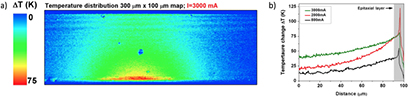
Figure 13. (a) Temperature distribution map (300 µm × 100 µm) of the facet of the degraded DL operating at I = 3000 mA. (b) Comparison of the temperature change across the facet for non-degraded (I = 2000 mA-dark gray line and 800 mA-black line) and degraded device (I = 3000 mA, light grey line). © [2007] IEEE. Reprinted, with permission, from [107].
Download figure:
Standard image High-resolution imageIt can be noticed that the temperature distribution presented in figure 13 differs from the one measured before degradation (figure 12). This difference is better visible if we compare the vertical line scans across the facet at different driving currents 800 mA and 2000 mA (device lasing) and for 3000 mA (no laser emission). It can be observed that in case of emitting structure the line scan across the facet in the range from 0 µm to 93 µm (GaAs substrate) has exponential shape typical for heat diffusion, but in the region from 93 µm to 100 µm (epitaxial layer) rapid increase of the temperature change is observed. In case of not lasing device (3000 mA) this rapid increase of the temperature in the active region is not observed. Also, the change of temperature of the GaAs substrate is higher for 3000 mA. Results shown in figure 13(a) indicate that the facet temperature of the damaged laser is substantially lower than for the same device before failure. This observation can be explained by the fact, that after degradation there is no reabsorption of light on the mirror. On the basis of experimental results, it can be said that optical contribution to facet heating caused by reabsorption of photons is strong mechanism in laser devices especially at high output optical powers. It becomes negligible for non-operating devices, as the temperature induced degradation path is accelerated by high optical power density at mirror of the laser chip [107].
5.1.3. Thermoreflectance measurements of the in-laser diodes with non-injected facet (NIF).
Temperature distributions on the facets of devices of modified design: non-injected facet (NIF) lasers, were compared with standard construction to confirm experimentally the effect of reduction of mirror temperature. NIF construction is characterised by the fact that metal contact is retracted from facets by the distance of few tens of microns (here ca 40 µm, forming area in which current is not injected. This results in reduction of surface nonradiative recombination on mirrors in NIF device by limiting the lateral diffusion of injected carriers.
The optical power-current and current–voltage characteristics of both groups of lasers are very similar. The threshold current for NIF laser equals Ith = 0.320 A whereas for standard laser it equals Ith = 0.398 A [108].
In order to compare temperature distribution profiles in the facet region being exposed to the optical damage, probe beam of 405 nm (3.06 eV) was used [108, 109]. As discussed in calibration section, for this energy, we can expect the maximum thermoreflectance signal to originate from the active and waveguide region composed mainly of AlGaAs.
Figure 14 presented below, shows temperature maps for NIF (a) and standard (b) laser diodes operated at 1200 mA. Higher temperature is observed in case of standard LD. To compare quantitatively temperature distributions for both laser constructions figure 14(c) presents relevant, lateral cross-sections in junction plane.
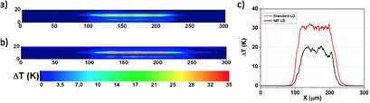
Figure 14. Temperature distribution 300 µm × 20 µm maps of the NIF laser facets operated at 600 mA (a) and standard laser (b). Comparison of temperature distributions across the facet of NIF and standard lasers operated at 600 mA current (c). Reproduced with permission from [108].
Download figure:
Standard image High-resolution imageThe maximum change of temperature for NIF laser is T = 20 K and for standard laser diode T = 30 K. This result shows that NIF laser design allows decreasing of facet temperature compared to standard device. Reducing surface recombination by decreasing the carrier injection in the vicinity of mirror results in decreased temperature rise and smaller bandgap shrinkage. This in turn results in lower reabsorption of radiation.
We have used thermoreflectance spectroscopy to measure temperature distribution over the facet of semiconductor lasers. Results were used to monitor influence of mirror treatment, mounting as well as construction of the device on the temperature rise on the facet. Temperature data can be registered as 2D maps or 1D linescans. TR technique can also be used to monitor temperature of specified point on the facet of the device. Temperature data provides information about thermal processes, optical and current contributions to facet heating and degradation processes. Presented results confirm capability of TR technique to provide information with high spatial resolution of about 1 µm and temperature resolution better than 1 K [108].
5.2. Thermal properties of high power laser bars
The study of thermal properties of High Power Semiconductor Laser Bars allowing the identification of emitter failure mechanisms and providing insight into heat management of the devices has been performed by means of thermoreflectance spectroscopy to obtain high resolution temperature distribution map over the facet of individual emitters.
The investigated device was high power 10 mm laser bar consisting of 25 emitters with 200 µm wide stripes [103, 110, 111]. The individual emitters are separated by 50 µm wide optically and electrically isolated area. The device was mounted 'epi-side down' onto a Cu heat sink. The threshold current for CW operation at 25 °C was equal to 12 A; the slope efficiency was 1.25 W A−1, the maximum output power was 60 W. Figure 15 presents images and scheme of the laser bar structure.
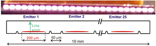
Figure 15. Images of the operating laser bars registered by CCD camera in the TR set-up and scheme of the investigated high power laser bar. Reprinted from [111], Copyright 2009, with permission from Elsevier.
Download figure:
Standard image High-resolution imageThe line-scans starting at the active region towards substrate were measured in the center of each emitter. The laser bar were operated in quasi-CW mode with square current pulses of amplitude up to 40 A. The temperature of the heat sink was stabilized at 25 °C. Figure 16 shows exemplary line-scans presented in the same scale.

Figure 16. Temperature line-scans for emitters no. 4, 5 and no.22. (ITE unpublished result).
Download figure:
Standard image High-resolution imageFigure 17 shows the maximum of temperature increases obtained for GaAs substrate at the interface with epitaxial layers and at the center of active region for each emitter of the laser bar.
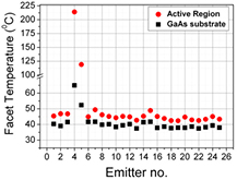
Figure 17. Comparison of the maximum temperature increases for GaAs substrate and the active region for each of the laser bar. [103] 2008 © Springer Science+Business Media, LLC 2008. With permission of Springer.
Download figure:
Standard image High-resolution imageThe values of temperature increase for each emitter were similar, except for the emitters no. 4 and no.5 The subsequent studies were devoted towards explanation of different temperature behavior of these emitters/emitter no.4 and 5. The temperature distribution maps of both emitters are shown in figure 18.
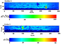
Figure 18. Temperature distribution map (300 µm × 30 µm) for emitter no.4 and 5, at supply current 40 A. (ITE unpublished result).
Download figure:
Standard image High-resolution imageMaps show pronounced degradation of the facets and large hot spots at x = 225 µm (for emitter no.4) and at x = 100 µm (for emitter no.5). The presence of the hot spot at the facet of the emitter indicates the ongoing mirror degradation process, which eventually leads to COMD failure. From the previous studies of similar cases [112] it is known that emitter failure creates thermal runaway, gradually leading to destruction of the whole device. The increase of the mirror temperature at the hot spot (ΔT = 200) already poses a serious danger to the device because of the positive feedback mechanism governing the COMD process.
In the next step the near-field intensity distribution was recorded with a silicon CCD camera and examined for all emitters in the array. Typically for broad-area devices, the emitters show a multi filamentary near-field distribution with almost equal intensity along the bar. Looking more closely, however, dark areas indicating a reduced interband recombination could be observed at the near-field patterns of some emitters. This is illustrated in figure 19(a) which shows the nearfield pattern of emitter no. 4, that exhibits some defects around 225 µm. Figure 19(b) once again presents temperature distribution map of the area around the active stripe area for emitter no. 4, at (x = 225 µm) with hot spot on the right-hand side.
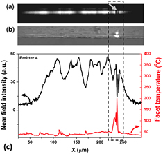
Figure 19. (a) Near-field pattern for emitter no. 4 recorded by a CCD camera. (b) Thermoreflectance map recalculated to temperature for the same emitter (scanned area is 300 µm × 30 µm) and (c) horizontal cross-section (in-junction plane). [103] 2008 © Springer Science+Business Media, LLC 2008. With permission of Springer.
Download figure:
Standard image High-resolution imageComparison of near field emission pattern for this emitter with a horizontal cross-section of temperature map along the active region are presented in the figure 19(c). From this comparison, it can be seen that the higher values of temperature occur where the dark spots are located. In such points, almost all electrical power is converted into heat which additionally changes junction voltage and further increases the local current density. This effect is known as current crowding [103, 111].
Highly spatially resolved information about temperature along the active stripes of all the emitters in the bar was obtained from thermoreflectance data. The recorded maps revealed multiple hot spots localized in the active area region of the laser structure.
In order to obtain full information about the state of the facets the temperature distribution has to be mapped at least over the of whole active region, as the hot spots can easily be missed when recording only line-scans. It was found that the presence of the hot spots at the mirror facets is an indicative of the ongoing degradation process. This is equally true for single emitters as well as for laser bars, although in the latter case this can have serious consequences not only to particular emitter but to the device as a whole since the failure of the emitter creates thermal runaway, gradually destroying the whole device.
Apart from the thermoreflectance, thermal properties of the laser bars were also studied by two complementary thermometric techniques; IR thermography which provides fast information about temperature profiles and hot spot locations and wavelength tuning technique which is used to determine the time-resolved bulk temperature for all emitters in the bar [103]. Analysis of the results obtained by different methods indicate that the observed local overheating is related to defects starting at the laser facet or very close to the facet. Thermoreflectance is capable of spatially resolved 'hot spot' detection at the vicinity of the facets of high power laser bars.
5.3. Quantum cascade lasers (QCL)
QCLs are the most advanced class of semiconductor sources operating in the mid-infrared (IR) (3.5 µm–24 µm) and terahertz region (1 to 5 THz) [113]. QCL was demonstrated in 1994, by the pioneering work from Federico Capasso's group [114] at Bell Labs (USA). The physics behind optical transitions of a QCL differs from that of a diode laser. In a QCL the lasing transitions occur between states within conduction band of a coupled quantum well system. QCLs are based on intersubband transitions between states created by quantum confinement in ultrathin alternating layers of semiconductors. By contrast, in a diode laser transitions occur between the conduction band and valence band of the semiconductor material. Figure 20 shows TEM picture of top part of QCL heterostructure.
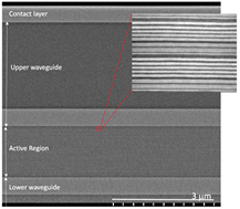
Figure 20. TEM picture of top part of QCL heterostructure. Clos-up shows the individual layers forming two periods in active region. (ITE unpublished result).
Download figure:
Standard image High-resolution imageLarge electrical power density required for their operation and low thermal conductivity of complex, multilayer heterostructure lead to strong local heating effects inside the device active region. Elevated temperature of active core result in significantly lower efficiency of QCLs, especially if high temperature operation is considered. These are the main limiting factors of high temperature operation of the devices [115]. Thermal management problems are still not solved in such devices; therefore, direct methods of probing temperature distribution in the devices are very important for the optimization and possibly improve the reliability and lifetime of the QCL.
Thermoreflectance measurements of QCL started in at the Institute of Electron Technology in 2005 and lead to the ability to register temperature distribution over the facet of QCL [116]. In the next papers [117–119] different mounting options and device geometries are compared in terms of their influence on the relative increase of the active region temperature. The numerical thermal model of QC lasers, solving heat transport equation in 2D and 3D, which includes anisotropy of thermal conductivity was developed [120]. By combining experimental and numerical results, an insight into thermal management in QCLs is gained. Thermal optimization of the design focuses on improving heat dissipation in the device, which is essential to increase performance of devices. Application of CCD thermoreflectance spectroscopy as a tool for thermal characterization of QCL was presented in 2016 [84].
In this section results of investigation of thermal properties of QCLs by means of CCD TR will be presented. The measurements enable: (A) analysis of influence of different operating conditions (B) study the influence of device geometry on its thermal properties, (C) investigation of influence of mounting technology on its thermal properties and (D). The examined structures are the QCLs grown by MBE at the Institute of Electron Technology in Warsaw based on GaAs [121–123] as well as InP [124, 125] material systems.
5.3.1. Influence of operating conditions on the QCL temperature.
In order to gain insight into the thermal management in QCLs we have examined the influence of different operating conditions on the temperature of devices. Heat load in the devices was changed by changing pulse width at constant frequency or amplitude of driving current.
Maps presented in figures 21 and 22 present the front facet of AlGaAs/GaAs QCL. Maps are presented in the same temperature scale. The image area is 80 µm wide and 40 µm high, and covers the area around the active stripe including two etched trenches. Temperature distribution maps show a temperature rise over the heatsink temperature stabilized by the TE cooler. The measurements were performed for different values of driving current and pulse width. At the bottom of the maps are the epitaxial layers, with an active region (between trenches) and interface with copper heatsink [84].
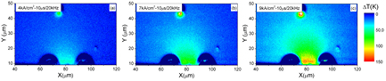
Figure 21. Temperature distribution maps on the front facet of a GaAs/AlGaAs/GaAs QCL, registered for device operated at a constant pulse width, 10 µs and a frequency 20 kHz for different values of driving current density: (a) 4 kA cm−2, (b) 7 kA cm−2 and (c) 9 kA cm−2. Reproduced from [84]. © IOP Publishing Ltd. All rights reserved.
Download figure:
Standard image High-resolution image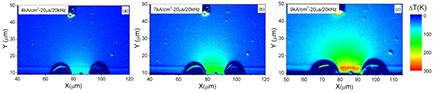
Figure 22. Temperature distribution maps on the front facet of a GaAs/AlGaAs/GaAs QCL, registered for device operated at a constant pulse width, 20 µs and frequency 20 kHz for different values of driving current density: (a) 4 kA cm−2, (b) 7 kA cm−2 and (c) 9 kA cm−2. Reproduced from [84]. © IOP Publishing Ltd. All rights reserved.
Download figure:
Standard image High-resolution imageIt can be observed that with the increase of the supply current, the maximal temperature in the active region rises substantially and the heat is spreading further into the substrate towards the laser upper contact [84].
5.3.2. Study of the influence of device geometry on its thermal properties.
Influence of different mesa dimensions on lattice-matched AlInAs/InGaAs/InP QCLs on thermal properties was investigated. Figures 23(a)–(f) presents temperature distribution maps on the front facet of QCL and maximal temperature increases, registered for devices operated at constant current density 5 kA cm−2, pulse width 10 µs and frequency 20 kHz for different mesa dimensions in the range from 5 µm to 35 µm. In general, the shape of the temperature distribution does not depend on the mesa dimensions. For all investigated devices, heat is localized in the active area and poor dissipation into the substrate can be seen. It can also be observed that for QCLs with narrower mesas, lower temperature increases occur for the same value of current density, compared to the QCLs with wider mesa (figure 23(f)). This fact is connected with the volume of the active core; for narrow mesa device, the absolute current for a given current density is lower which results in lower dissipated electrical power and consequently lower heat generation.
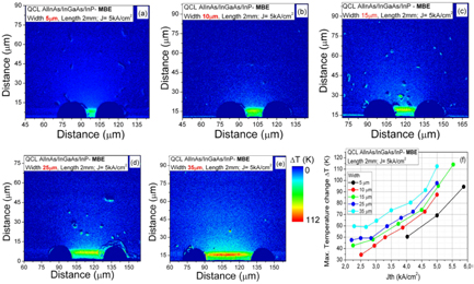
Figure 23. Temperature distribution maps on the front facet of QCL, register for device operated at a constant current density 5 kA cm−2, pulse width 10 μs and frequency 20 kHz for different mesa dimensions change in the range from 5 μm (a) to 35 μm (e). Maximal temperature increases as a function of current density for devices under test (f). Reproduced from [84]. © IOP Publishing Ltd. All rights reserved.
Download figure:
Standard image High-resolution image5.3.3. Investigation of influence of mounting technology on its thermal properties.
Influence of mounting technology on the device heating was studied experimentally. In experimentally determined temperature maps and profiles, excessive facet heating associated with the lack of thermal contact with heat sink in the region of the facet of the laser was observed. Detailed study of this specific issue is presented in [120]. Since TR is a technique giving information about surface temperature, it shows very well disturbed shape of heat diffusion, due to overheating of the part of the laser without good thermal contact with the heatsink. Figure 24 shows temperature map of incorrectly soldered device. Compared to results shown in figure 23, different shape of temperature distribution is observed. This difference in heat dissipations stems from the lack of thermal contact in the region of mirror.
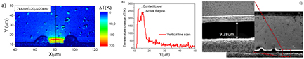
Figure 24. (a) Experimental temperature distributions maps on the front facet of QCL and (b) vertical profile in the center of active area. (c) SEM photograph presenting defective mounting of the device under study, resulting in relatively large gap between laser chip and the submount. (ITE unpublished result).
Download figure:
Standard image High-resolution imageExperimental results are in good agreement with numerical simulation. Numerical simulation shows, that lack of thermal contact at mirror, can lead to significant overheating of part of laser close to the mirror [120].
5.3.4. Comparison of thermal properties: GaAs/AlGaAs/GaAs and AlInAs/InGaAs/InP QCLs.
Figure 25 presents comparison of temperature distribution maps and line scans for GaAs/AlGaAs/GaAs and AlInAs/InGaAs/InP QCLs. The shape of the temperature distribution on the front facet on InP-based QCLs differs significantly from the one registered for GaAs-based QCLs. The heat is accumulated in the active area with small heat dissipation towards the substrate. It can be seen better in the temperature distribution line scans across the facet at the center of the active area presented in figure 25(c).
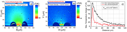
Figure 25. Temperature distribution maps on the front facet of GaAs/AlGaAs and AlInAs/InP QCLs, registered at the same operation conditions. Temperature distribution line scans across the facet, taken at the center of the active area perpendicular to the epitaxial layers for two types of QCLs. Reproduced from [84]. © IOP Publishing Ltd. All rights reserved.
Download figure:
Standard image High-resolution imageThe reason for the lack of heat flow towards the substrate is connected with the In0.53Ga0.47As layers present in the design. The role of those layers is to increase the optical mode confinement and its overlap with the active core. However, InGaAs with ~50% of In is characterized by dramatically reduced thermal conductivity in the order of 5 W m−1 K−1, which is roughly a factor of 10 less than for InP [126, 127]. The other reason is that InP thermal conductivity is higher than GaAs, resulting in more efficient dissipation of heat.
QCLs were investigated in a standard TR experiment as well as with CCD implementation of TR.
The measurement was done for the same device at the same operating conditions in both experiments. Figure 26 presents two temperature distribution maps registered with standard TR—figure 26(a) and CCD TR—figure 26(b). Maps registered by CCD TR contain more data points, separated by a smaller distance. In other words, the temperature data is sampled in more points than in the case of scanning TR, thus providing a clear, sharp image of the laser facet, with no measurement artifacts, as opposed to the standard TR result. The imaging capabilities of CCD TR, providing a higher density of measurement points, are important for devices having features of small dimensions in the range of a few micrometers. In such cases CCD TR implementation is much better suited, especially because its imaging area depends on the magnification of the optical system and can be easily adjusted by using objectives of different magnification.

Figure 26. Temperature distribution maps registered by standard thermoreflectance spectroscopy (a) and CCD thermoreflectance (b). QCL operation conditions are the same 6 kA cm−2/20 µs/20 kHz. Reproduced from [84]. © IOP Publishing Ltd. All rights reserved.
Download figure:
Standard image High-resolution imageAs can be observed in maps (figure 26), results obtained with both techniques present good agreement in terms of reconstruction of the temperature distribution on the facet of the QCL, as well as the value of the temperature is in agreement between both implementations. It is worth emphasizing, that in case of CCD TR, time required for acquisition of the map presented in figure 26(a) was ca. 13 s, whereas in case of standard TR, the map shown in figure 26(b) was registered in ca. 2 h.
CCD TR is perfectly suited for the case of investigation of QCLs. Due to emission wavelength, far beyond the detection of silicon sensor of camera, there is no need to use filters cutting of unwanted laser radiation, as it is in the case of lasers emitting in visible or near-IR part of spectrum. Since CCD TR involves frame averaging, even small amount of unfiltered lasing will become visible in registered data, making detection of real thermal information very difficult.
The information extracted from thermoreflectance experiments prove to be very useful in determination of thermal properties of the examined QCLs, providing information on heat sources localization and extent as well as heat dissipation. It is used for monitoring of mounting and its possible faults. The experimental results also provide data for a numerical simulation of QCL's thermal properties.
5.4. Vertical external cavity surface emitting lasers (VECSEL)
Optically pumped vertical-external-cavity-surface emitting lasers (VECSELs) combine the properties of semiconductor lasers and classical solid state lasers, offering high optical output power in circular, nearly diffraction limited beams [128, 129].
Because of optical pumping, major constraints on the performance of VECSELs are thermal. Temperature affects the performance of VECSELs in a number of ways. Elevated temperatures affect the material gain and loss mechanisms, e.g. thermally excited carriers are more likely to escape the quantum wells (QWs). Also, the main structural features, namely, the distributed Bragg reflector (DBR) mirror reflectivity band and the micro-cavity resonance, as well as the QW gain spectrum shift with temperature at different rates, causing these key components to move away from one another, as the temperature rises.
The amount of waste heat generated by optical pumping depends on so called quantum defect, defined as the difference in energy between pump and VECSEL emission. In case of VECSELs emitting in 2.1 micrometer range, which are pumped by 980 nm pump laser, quantum defect reaches 50%, resulting in a large amount of heat generated in the structure.
Waste heat from pumping can be extracted through the DBR and the substrate. Both the substrate itself and the DBR cause significant thermal resistance. Two main approaches have been proposed in order to overcome this problem: substrate removal [130] and the application of an intracavity heatspreader made of high thermal conductivity material [131].
TR was used to characterize thermally different approaches of heat removal from VECSEL chip. Experimental results on temperature of devices were used to confirm assumptions of numerical models of heat dissipation in VECSELs.
Due to specifics of the external cavity laser, the TR experimental setup had to be designed to accommodate gain chip, external mirror and pump optics. The straightforward solution was to construct angular configuration TR setup (V-TR), allowing measuring temperature distributions on the surfaces of VECSEL chips. This setup configuration is shown in figure 27(b). In this setup, the probe beam is introduced at an angle to the surface of the device, and is collected at an angle after reflection.
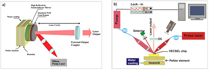
Figure 27. (a) Scheme of the optically pumped VECSEL. (b) Scheme of the V-TR configuration of the thermoreflectance experimental setup. The VECSEL chip clamped into a copper sample holder is mounted on the temperature stabilized heatsink, placed together with the pump optics and the external cavity on the motorized x-y-z stages. Reprinted from [133], with the permission of AIP Publishing.
Download figure:
Standard image High-resolution imageLowering of the temperature was registered for device with intracavity silicon carbide (SiC) heatspreader [132, 133] as predicted by numerical modelling and actual laser measurements [134, 135].
Heat balance of VECSELs assumes that we can expect lowering of temperature of device due to emission of light (lasing). To register the effect, measurements were performed twice for each device: once during lasing, and once when it was being prevented from lasing by introducing an element into the cavity, blocking the mode propagation. Both standard chip as well as chip with SiC heatspreader were tested.
Figure 28 presents maximum temperature increase over the heatsink temperature of 228.5 K observed at the center of the VECSEL chip. The difference (OFF-ON) reaches 2 K (which is roughly 1%) and is a consequence of the fact that part of the pump energy is extracted from the device in the form of laser emission.
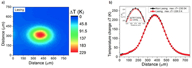
Figure 28. Temperature distribution map for operating VECSEL without SiC heatspreader. (b) Comparison of radial temperature profiles for lasing and non-lasing device (right). Reprinted from [133], with the permission of AIP Publishing.
Download figure:
Standard image High-resolution imageFor VECSEL with a SiC heatspreader temperature distribution map and the temperature profiles are presented in figure 29. Maximum temperature increase is 30 K for the nonlasing device and 25 K in the case of the lasing VECSEL. The difference between lasing and non-lasing VECSELs is 5 K, which is about 17%. The small relative decrease of the VECSEL temperature is in this case the result of a lower absolute value of emitted power under the same pumping conditions. It also should be stressed that the overall temperature increase for the VECSEL with a heatspreader is approximately 10 times lower than that for the device without a heatspreader, and the consequent radial temperature profiles are wider due to the enhanced lateral heat spreading.
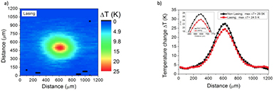
Figure 29. (a) Temperature distribution map for operating VECSEL with SiC heatspreader. (b) Comparison of radial temperature profiles for lasing and non-lasing device. Reprinted from [133], with the permission of AIP Publishing.
Download figure:
Standard image High-resolution imageFigure 30 shows a comparison of the temperature increases for operating and nonoperating VECSELs without and with a SiC heatspreader versus the average energy of pump laser per cycle.
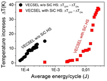
Figure 30. Difference in the maximal temperature increases between lasing and non-lasing devices without a heatspreader (circles) and for VECSEL with A SiC heatspreader (squares). Reprinted from [133], with the permission of AIP Publishing.
Download figure:
Standard image High-resolution imageFor the VECSEL without a heatspreader, it can be seen that for an average energy per cycle of 4.5 × 10⁻⁴ J, temperature increase equals 15 K, whereas for VECSEL with a SiC heatspreader temperature increase equals 0.5 K.
The implementation of the thermoreflectance technique for the thermal analysis of VECSELs was demonstrated. It allowed us to determine experimentally the temperature distribution in operating VECSELs for various operating conditions and different cooling schemes. It was found that during operation, the device exhibits a lower temperature due to the effect of the conversion of pump power to useful emitted radiation. The higher the VECSEL output power, the larger the temperature difference in reference to the non-emitting case. The influence of a heatspreader on the VECSEL temperature was experimentally investigated, and the results confirm the effectiveness of this approach in lowering the device's temperature and increasing its performance. The devices with an intracavity SiC heatspreader exhibit much lower temperatures (by a factor of ten) and wider temperature profiles connected with lateral heat spreading due to the high thermal conductivity of the heatspreader material [133].
5.5. GaN based diode lasers
Nitride based, wide-bandgap semiconductors attract great interest as materials for light emitting devices in the blue to ultraviolet wavelength region [136–138]. The first demonstration of emission in GaN-based laser diode was reported in 1996 by Nakamura [139, 140]. Still, their maximum optical power, lifetime and reliability are strongly limited by degradation processes induced mainly by increase of the temperature in the particular parts of the laser: facet, active layers or contacts [141–143]. Typical degradation mechanisms known from arsenide based devices (like COMD or DLD) are not responsible for failure of GaN based diodes. The threshold of COMD was determined to be around 40–57 MW cm−2 for InGaN laser diodes [144, 145]—an order of magnitude higher than for GaAs counterparts.
Despite intense investigation of InGaN laser diodes, mechanisms responsible for degradation have not been fully identified and agreed on. The factor that is generally considered as the major source of degradation is current injection.
Some experimental reports include investigations of thermal properties of GaN based laser diodes performed by electroluminescence or PL [146, 147] micro-Raman spectroscopy [148] or thermal imaging [149].
The main goal of using TR to study GaN-based lasers was to register temperature evolution up to the degradation point.
The experimental part is more problematic than in case of previous types of devices. In order to conduct measurements, probe beam energy has to be above the material's bandgap, otherwise, the crystal becomes transparent, what renders the experiment impossible. As source of the probe beam the 355 nm (3.5 eV) laser was used, above GaN bandgap of 362 nm (3.42 eV). The choice of probe beam wavelength affected the choice of optics of TR setup, as it had to be adapted to ultraviolet light. Also, appropriate optical filters had to be used to cut-off the lasing wavelength of the examined device.
The investigated structures were grown by MOCVD on bulk GaN crystals. Devices were processed into oxide isolated, ridge waveguide devices with stripe dimensions of 3 × 700 µm.
The influence of operating conditions (various bias currents and duty cycles) on the temperature value and distribution was studied. Figure 31 presents temperature distribution map, covering the area of 110 × 110 µm. The maximal temperature increase equals ΔT = 16 K and takes place close to active region layers. The heat generated in the active layer is conducted to the heat sink through the GaN substrate. The shape of the temperature distribution implies good dissipation of heat generated in the active region, due to high thermal conductivity of the GaN substrate.
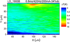
Figure 31. Temperature distribution map on the front facet of GaN based laser, registered for device operated at pulse width 800 µs and frequency 420 Hz and driving current of 200 mA. Reproduced from [151]. CC BY 4.0.
Download figure:
Standard image High-resolution imageThe heat load in the device was changed by changing the amplitude of the driving current at constant frequency and pulse time. For such experimental conditions, temperature distribution line scans were registered at the centre of the active area perpendicular to the epitaxial layers. Figure 32(a) presents line scans for device operated in bias current range of 120 mA–360 mA. It can be observed that for all bias currents, maximum temperature increases are localized in the active area, and at about ~15 µm towards heatsink decrease to the temperature of GaN substrate which is almost uniform. The maximum temperature increases versus driving current registered for epitaxial layers and GaN substrate are presented in figure 32(b). Maximum temperature increases registered at bias I = 360 mA for active area equal 47 K and 17 K for GaN substrate.
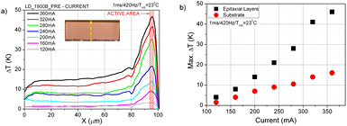
Figure 32. Temperature distribution line scans across the facet, taken at the centre of the active area perpendicular to the epitaxial layers for different driving current. (b) Maximum temperature increases versus driving current registered for epitaxial layers and GaN substrate. Reproduced from [151]. CC BY 4.0.
Download figure:
Standard image High-resolution imageTemperature rise during extreme operation conditions was registered, eventually leading to catastrophic degradation of the laser. Temperature rise was registered as the amplitude of the bias current was gradually increased up to the point of degradation of the DL. It should be mentioned, that range of bias currents used in this experiment is far beyond standard operation conditions of GaN-based devices (typical bias current of CW devices is in the range below 200 mA). The reason for this is the fact, that in order to register fatal degradation of a laser, it has to be operated at maximal ratings or beyond. Apart from this, since current is expected to be the major driving force of degradation, at high ratings of bias current observation of enhancement of processes leading to failure is expected. Temperature line scans are presented in figure 33(a). The bias current was increased, up to measurement of the line scan for I = 720 mA, when degradation of DL occurred, resulting in ceased optical emission from the device and operating voltage decreased by a factor of 2. Then, measurement was repeated for the same bias current. The comparison of two line scans registered for 720 mA of bias current is presented in figure 33(b) and denoted as I and II, respectively. The third line scan (III) presented in figure 33(b) was measured after the optical emission has stopped, for higher bias current of 820 mA. During measurement III, the device underwent catastrophic degradation.
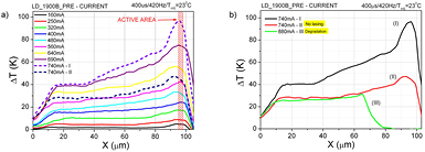
Figure 33. Temperature distribution line scans across the facet, taken at the centre of the active area perpendicular to the epitaxial layers for different driving current. (b) Comparison of temperature distribution line scans for 720 mA driving current for DL operating at normal condition (black line), for DL which has ceased lasing (red line) and for degraded device (green line). Reproduced from [151]. CC BY 4.0.
Download figure:
Standard image High-resolution imageFigure 34 presents comparison of maximal temperature increases registered in the active region for investigated DL. Points labelled as (I)–(III), correspond to line scan measurements as described earlier.
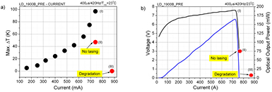
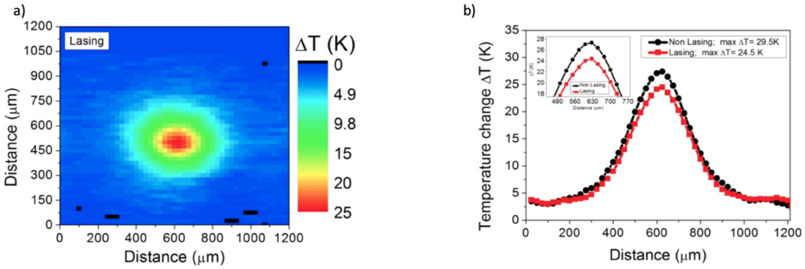
Figure 34. Maximum temperature increases versus pulse width registered for epitaxial layers and GaN substrate. Reproduced from [151]. CC BY 4.0.
Download figure:
Standard image High-resolution image
Significant reduction (by a factor of 2.1) of maximal temperature in case of points I and II is observed. For point II, as the device is not emitting, there is no contribution of optical reabsorption to the temperature rise. The temperature registered in this case is almost twice lower than in the case of measurement I. Electrical power delivered to the device in case of measurement I was ~5.2 W, whereas for measurement II it has dropped to 2.6 W. On the basis of experimental results, it was concluded that contribution of reabsorbed light into the total temperature is negligible. It should be mentioned that LDs were fabricated to have metallic contact retracted from the facet, to form non-injected regions close to mirrors, reducing significantly surface carrier recombination. The reabsorption of emitted radiation was found to be negligible due to relatively low optical power emitted by the investigated device (~160 mW). In such conditions the threshold for COMD could not be reached. This is also supported by lifetime tests, conducted below threshold as well as above, indicating no correlation of degradation rate with the effect of reabsorption of laser emission [150]. Furthermore, temperatures registered at the facet, suggest, that high temperature of the junction is not responsible for degradation. The maximal temperature rise observed reaches 100 K, meaning that in the absence of reabsorption of radiation temperature inside the resonator is comparable to the one observed at the facet, mostly due to high thermal conductivity of GaN (heat is efficiently dissipated). However, experimental results cannot exclude high, local temperature rise inside resonator, taking place in the vicinity of e.g. built-in defect. The microscopic investigation of degradation included examination of DL by means of scanning electron microscopy (SEM), as well as destructive focused ion beam (FIB) etching was applied, revealing internal defects formed within the cavity [151].
6. Conclusions
In this work the application of TR to investigate the thermal properties of different types of lasers was discussed. It was shown, that TR is a versatile technique that can be adapted to various geometries of lasers, materials and operating conditions. TR was used to monitor mounting options of lasers and their influence on temperature distribution and heat dissipation paths. This is useful also in case of faults that can be introduced to thermal contact between chip and heatsink/heatspreader during the last stage of fabrication of the device. It was shown, that improper mounting leads to increased facet temperature due to the lack of thermal contact between semiconductor chip and submount. It was possible to monitor how surface treatment influences the mirror temperature, which depend on the density of surface defects. By means of TR, it is possible to register effects of heat balance, as it was the case in VECSELs.
CCD TR is perfect for the study of properties of devices that do not emit light registered by the camera's sensor. Otherwise, analysis of experimental data becomes problematic.
From the overview of the problems presented in this review, it becomes clear, that the problem of heat in laser devices is still 'new' and will be for future generations of optoelectronic components.
Acknowledgments
I would like to thank Tomasz Ochalski and Tomasz Piwoński for introducing me to the field of optical spectroscopy and their contributions to TR development in ITE. Prof Maciej Bugajski is acknowledged for stimulating me to perform the work and finally publish it, as well as for many discussions and comments. I would like to thank Kamil Pierściński for supporting experimental works with numerical simulations and all colleagues from ITE for participating in works over the years.
Special thanks are due to Jens W Tomm for many discussions concerning laser degradation and characterization methods. Parts of the results reported in the review were possible because of the involvement of Jens W Tomm in cooperation with the author.
Anna Kozłowska is acknowledged for her contribution to the work concerning laser bars. I would like to acknowledge Joachim Wagner, Marcel Rattunde, David Burns, John-Mark Hopkins for cooperation in VERTIGO EU FP6 project on VECSELs. Andrzej Malag, Piotr Perlin and Łucja Marona are acknowledged for providing lasers for experiments and their input to interpretation of results.
This work was financially supported by National Science Center (NCN) under projects no. 2015/17/B/ST7/04015 (OPUS) and 2011/03/D/ST7/03093 (SONATA).