

Abstract
Ag nanoparticles (NPs) and a CdSe nanocrystal were successively deposited on the surface of a TiO2 nanotube array film (CdSe/Ag/TiO2 NTs) via microwave assisted chemical reduction and in situ fabrication methods. The nanotubular structure of TiO2 preserves well after loading Ag and CdSe, as the ternary composite not only exhibits an excellent visible light harvesting ability but also has the smallest charge transfer resistance according to electrochemical impedance measurement. The most positive flat band potential of CdSe/Ag/TiO2 NTs facilitates charge carrier transfer at the semiconductor-electrolyte interface. Notably, the introduction of Ag nanoparticles forms a unique carrier-transfer-channel in the CdSe/Ag/TiO2 NTs system, in which the Ag nanoparticles can take advantage of its high carriers transfer rate as a linker. In addition, Ag serving as a surface plasmon resonance source further improves photoelectric catalytic activities of the sample. It is noteworthy that CdSe/Ag/TiO2 NTs exhibits the desired photoelectrochemical performance with the highest H2 production rate of 413.99 µmol cm−2 after 2.5 h irradiation.
Export citation and abstract BibTeX RIS
1. Introduction
Energy crisis and environmental pollution problems have increasingly emerged as key obstacles for global sustainable development [1, 2]. There is an urgent need to develop clean energy from sustainable energy sources [3, 4]. Solar light as an abundant, renewable energy source can be converted and stored in the form of H2 via photoelectrochemical water-splitting [5, 6]. In the process of photoelectrochemical water splitting, H2 and O2 can be obtained from redox reactions of photo-induced electrons and holes pairs, respectively [7]. Therefore, it is essential to restrict the spontaneous recombination rate of photo-generated e− and h+ and facilitate charges transfer between semiconductors and electrolyte for improving the efficiency of water-splitting [8]. At the same time, exploitation of stable and efficient electrode materials is a great challenge for designing efficient photoelectrochemical water-splitting systems due to the crucial conditions.
TiO2 nanotube arrays (NTs) with corrosion stability, a stable nanotubular structure and excellent electron percolation pathways are a promising semiconductor material among those photocatalytic materials which have been widely utilized in photoelectrochemical H2 production from water decomposition [9–12]. However, the wide band gap of TiO2 (3.2 eV for anatase) limits their photoresponse to only 5% of sunlight energy in the ultraviolet range [13], and very high recombination rates of the photoinduced electron–hole pairs further lower the photoconversion efficiency [14]. The investigations focus on physical chemical methods for improving the light response range of TiO2 to visible light and reducing the recombination rates of the photoinduced charge carriers, including expanding the optical absorption of TiO2 by decreasing its energy band gap and changing its energy structure [15]. Particularly, coupling TiO2 with a narrow band-gap semiconductor has been increased progressively, in which desired photoelectrochemical properties emerge [16]. Recently, Liao et al deposited PbSe quantum dots on the surface of TiO2 NTs, providing an effective approach to expand light response and enhance the separation and interfacial transfer of charge carries [17]. Thanh Thuy et al synthesized ZnSe sensitized TiO2 NTs binary composites, exhibiting obviously improved activity for photocatalytic degradation of pentachlorophenol [18].
CdSe (1.7 eV), as an important II-VI semiconductor, has attracted considerable attention to modify TiO2 due to its wide absorption range and inimitable advantage. Xiao et al fabricated CdSe/TiO2 nanotube array nanocomposites through an electrochemical deposition strategy and revealed its photocatalytic and photoelectrochemical mechanism [19]. However, the low electron transfer rate still needs to be further improved, which results from poor conductivity between CdSe and TiO2 NTs [20]. As is well-known, the introduction of noble metals, such as Au, Ag and Pt with high carrier transfer rates, is an efficient strategy to solve that issue [21]. The noble metals can act as electron traps, promoting the interfacial charge transfer in the composite system [22]. Furthermore, noble metal NPs with a surface plasmon resonance effect are beneficial to the photocatalytic activities of TiO2 [21]. In this respect, Ag as an attractive candidate is introduced to our system because of lower material cost, facile preparation, high carriers transfer rate and the surface plasmon resonance effect [23].
In our previous works, CdSe sensitized TiO2 NTs (CdSe/TiO2 NTs) with improved photoelectrochemical performance were fabricated by an in situ fabrication method [24]. Different from the above work, Ag nanoparticles modified TiO2 NTs (Ag/TiO2 NTs) were firstly fabricated by a microwave-assisted chemical reduction route; then the CdSe nanocrystals were deposited on the surface of Ag/TiO2 NTs, which is expected to greatly enhance the hydrogen production efficiency of TiO2. A unique carrier-transfer-channel was formed in the composite system by Ag nanoparticles, which is beneficial for internal electron transfer. Meanwhile, the surface plasmon effect of Ag nanoparticles plays an important role in photoelectric catalysis processes. The sample CdSe/Ag/TiO2 NTs exhibits the best activity with a hydrogen production yield of about 413.99 µmol cm−2 for 2.5 h, which is 3.47 times than that of pure TiO2 NTs. In particular, the role of Ag in carriers transfer progress was studied in detail, which is responsible for enhanced photoelectrochemical performance.
2. Experimental
2.1. Preparation of samples
The TiO2 NTs films were prepared by a facile two-step anodization of Ti foil. The detailed routes and conditions of anodization preparation of TiO2 NTs are reported in our previous work [24]. The amorphous TNs were calcined at 450 °C in atmosphere for 2 h to convert to anatase phase. Ag/TiO2 NTs were fabricated via microwave assisted chemical reduction. In a typical synthesis, silver nitrate solution (0.005 M) was prepared (A solution). Then, 0.5 g polyvinyl pyrrolidone (PVP) and sodium hydrogen phosphite (0.0025 g) were put into 100 ml of polyethylene glycol in the beaker, stirring until transparent (B solution). After that, 20 ml of A and 20 ml of B solution were mixed and continuously stirred for 1 h, and then poured into a polytetrafluoroethylene (ptfe) tank. Subsequently, TiO2 NT films were immersed in the mixture solution and followed by a microwave reaction under 140 °C for 5 min to obtain Ag/TiO2 NTs. CdSe/TiO2 NTs were prepared by in situ fabrication, the same as the previous reported refluxing for 7 h [24]. CdSe/Ag/TiO2 NTs were prepared by loading a CdSe nanocrystal on the surface of Ag/TiO2 NTs. Detailed information about the preparation of TiO2 nanotubes and deposition of CdSe is shown in the supporting information (stacks.iop.org/JPhysD/51/305106/mmedia).
2.2. Characterization
X-ray diffraction (XRD) patterns were collected on a Shimadzu XRD-6000 powder diffractometer to characterise the crystalline structure of the samples. A scanning electron microscope (JSM-6390A) coupled with energy dispersive spectroscopy (EDS) was utilized to determine the morphology and elemental composition of the as-prepared composite samples. The microstructure, distribution, and the location of CdSe and Ag in the CdSe/Ag/TiO2 NTs samples were observed by high-resolution transmission electron microscopy (HRTEM). XPS spectra were acquired by Kratos AXIS NOVA to analyze the surface chemical states of samples. UV–vis diffuse reflectance spectra were obtained on a Shimadzu UV-3600 UV/Vis/NIR spectrometer equipped with an integrating sphere. Photoluminescence (PL) spectra were recorded on a fluorescence spectrophotometer (Hitachi-F7000) with an excitation wavelength of 220 nm to provide the recombination properties of photo-generated charge carriers.
2.3. Photoelectrochemical measurements
All of the obtained samples with a geometric area of 0.785 cm2 could be availably used as working electrodes for PEC performance tests, which were carried out on a CHI 660E electrochemical workstation at the 0.5 V bias potential with a solar simulator (100 mW cm−2). Ag/AgCl (saturated KCl) and platinum wire acted as the reference and counter electrodes, respectively. The electrolyte was a 0.5 M Na2SO4 solution.
2.4. Photoelectrochemical performance test
Photoelectrochemical water splitting was conducted in a three electrode system, where the reaction vessel was connected to a glass-closed gas-circulation system. A sealed quartz cell with the 100 ml electrolyte (0.35 M Na2S and 0.25 M Na2SO3) was carried out as a reaction place. A 300 W Xe lamp (340 mW cm−2) was utilized as the light source and the reaction system was subject to vacuum in a photoelectrochemical water splitting test. The evolved gases were analyzed using a gas chromatography (Tianmei, GC7900).
3. Results and discussion
XRD patterns of the samples are displayed in figure 1 to identify their crystallite phases. All diffraction peaks at 25.1°, 37.8°, 47.3°, 52.1° and 69.2° can be well indexed to the anatase TiO2 (JCPDS file no. 73-1764), shown to be highly crystalline. For CdSe loaded samples, CdSe related peaks are not observed due to their lower content [25]. The peaks at 37.7°, 43.7°, 63.3°, and 75.8° (JCPDS file no. 01-1167) of both Ag/TiO2 NTs and CdSe/Ag/TiO2 NTs patterns confirm that TiO2 NTs were successfully deposited with Ag NPs. It is worth noting that the intensity of the diffraction peak at about 37.8° becomes stronger compared with that of samples with no Ag existence, originating from the overlapping of TiO2 (0 0 4) and Ag (1 1 1) peaks [26, 27]. Similarly, there is no CdSe diffraction peaks in XRD patterns of CdSe/Ag/TiO2 NTs [28].
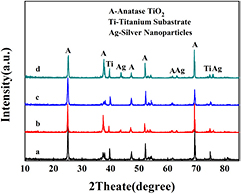
Figure 1. XRD patterns of (a) TiO2 NTs, (b) Ag/TiO2 NTs, (c) CdSe/TiO2 NTs and (d) CdSe/Ag/TiO2 NTs.
Download figure:
Standard image High-resolution imageSEM images of TiO2 NTs, Ag/TiO2 NTs and CdSe/Ag/TiO2 NTs were displayed in figure 2, as well as the EDX spectra and element mapping of CdSe/Ag/TiO2 NTs. It is obvious that TiO2 NTs with a unique tubular morphology were fabricated via two electrochemical anodization steps (figure 2(a)). Furthermore, it can be seen that Ag particles distribute on the orifices of TiO2 NTs and integrate with TiO2 NTs tightly (figure 2(b)). Besides, for the CdSe/Ag/TiO2 NTs sample, there are no obvious changes in the top and magnified views compared with Ag/TiO2 NTs, as shown in figure 2(c). Based on the corresponding EDX spectrum (figure 2(d)), the peaks of Ti, O, Ag, Cd and Se can be clearly observed, indicating that Ag and CdSe were introduced successfully. The atomic ratio of Cd and Se was found to be close to 1:1. The element mappings further demonstrate that both Ag and CdSe were evenly deposited on the surface of TiO2 NTs (figures 2(e)–(i)). Additionally, the surface of TiO2 NTs becomes rough after the deposition of Ag and CdSe, which is beneficial to contact with the electrolyte and lead to more efficient photoelectric chemical reactions.
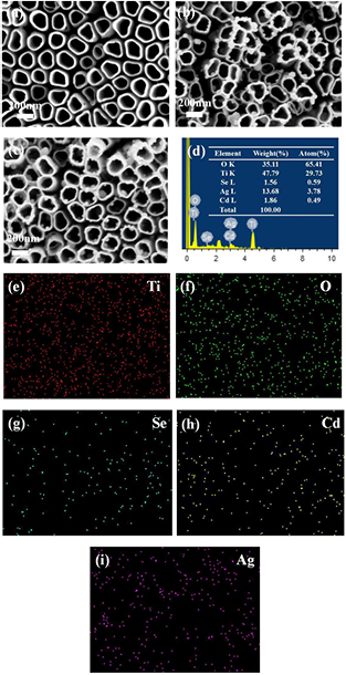
Figure 2. SEM images: (a) pure TiO2 NTs, (b) Ag/TiO2 NTs and (c) CdSe/Ag/TiO2 NTs; (d) EDS spectrum of CdSe/Ag/TiO2 NTs; the elemental mapping images for (e) Ti, (f) O, (g) Se, (h) Cd and (i) Ag.
Download figure:
Standard image High-resolution imageThe detailed microscopic structure was studied by HRTEM. It is shown that some nanoparticles are obviously deposited on the surface of TiO2 NTs (figure 3(a)). The HRTEM image in figure 3(b) shows three distinct sets of lattice fringes. The lattice fringes of 0.35 nm belong to the (1 0 1) lattice spacing of anatase TiO2, while the interplanar spacing of 0.238 nm is properly close to the (1 1 1) plane of Ag. The CdSe nanocrystal was observed with the interplane distance of 0.30 nm corresponding to the d-spacing of the (2 0 0) planes. Remarkably, it is apparent that CdSe, Ag and TiO2 could firmly contact with each other.
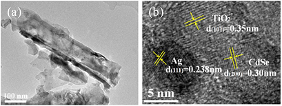
Figure 3. (a) TEM image of CdSe/Ag/TiO2 NTs (b) HRTEM image of CdSe/Ag/TiO2 NTs.
Download figure:
Standard image High-resolution imageTo further identify CdSe and Ag over TiO2 NTs, the surface composition and chemical states of film samples were characterized by XPS. As expected, the XPS analysis (figure 4(a)) confirms the existence of Ti, O, Ag, Cd, and Se in the composite. The signals at 458.9 eV and 464.5 eV, correspond to the Ti 2p1/2 and Ti 2p3/2, respectively (figure 4(b)), which demonstrates the species of Ti4+ in the sample [29]. Figure 4(c) exhibits two characteristic peaks of 405.5 eV and 412.3 eV, assigned to the Cd 3d5/2 and Cd 3d3/2 [30]. The peak at 53.9 eV is observed in the Se spectrum (figure 4(d)), which can be attributed to Se2− [31]. Those features reveal the presence of CdSe nanocrystal on the TiO2 NTs after in situ fabrication. On the other hand, the as-prepared sample presents two peaks at 367.9 eV and 373.9 eV (figure 4(e)), corresponding to 3d5/2 and 3d3/2 binding energies of Ag° metal, respectively, which indicates that Ag nanoparticles are deposited on the surface TiO2 films [32]. Based on the above analysis, it is demonstrated that Ag nanoparticles are successfully introduced in the ternary composite via the aforementioned synthetic routes, which is consistent with the results of EDS, element mapping and XRD.
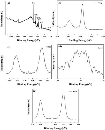
Figure 4. XPS spectra of the as-prepared CdSe/Ag/TiO2 NTs: (a) survey spectra, (b) high-resolution spectra of Ti 2p, (c) high-resolution spectra of Cd 3d, (d) high-resolution spectra of Se 3d and (e) high-resolution spectra of Ag 3d.
Download figure:
Standard image High-resolution imageThe absorption properties of the as-prepared samples were investigated by measuring the UV–vis DRS spectrum (figure 5). The characteristic bands of all the samples arising at approximately 387 nm should be attributed to intrinsic absorption of TiO2 [33]. There is almost no change on the absorption intensities after sensitized with CdSe or Ag, or both CdSe and Ag, nanoparticles in the UV range. Remarkably, the special absorption in the visible light region is observed due to the light scattering effect, which enhances the light harvest ability of all films [34]. Obviously, CdSe/TiO2 NTs and Ag/TiO2 NTs present the absorption in the visible light region, which is ascribed to the narrower band gap of the CdSe and surface plasmon effect of Ag, respectively. Significantly, CdSe/Ag/TiO2 NTs shows the best light absorption property in the visible light range because of the synergistic effect of Ag and CdSe.
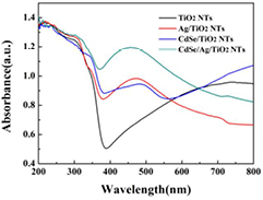
Figure 5. UV–vis diffuse reflectance spectra (DRS) of all samples.
Download figure:
Standard image High-resolution imageThe transient photocurrent is an efficient approach to estimate photoelectrochemical performance of as-prepared photocatalysts. As shown in figure 6(a), no photocurrent is observed in the dark and the rapid photocurrent is generated after imposing illumination. It is not surprising that all samples present sensitive photo-responses. Those photocurrent patterns can be repeated for five ON-OFF cycles, indicating their relatively corrosion stability. The Ag/TiO2 NTs and CdSe/TiO2 NTs exhibit higher photocurrent compared with that of pure TiO2 NTs at the 0.5 V bias potential, which is indicative of enhanced electron–hole separation. In particular, the transient photocurrent density of CdSe/Ag/TiO2 NTs is the highest, which is 3.64 times higher than that of TiO2 NTs, and it is also higher than that of Ag/TiO2 NTs and CdSe/TiO2 NTs. Clearly, Ag NPs and CdSe nanocrystal can boost the PEC performance of TiO2 for the surface plasma effect and heterojunction effect, respectively [35, 36]. In addition, the maximum photocurrent density of CdSe/Ag/TiO2 NTs results from the synergistic effect of Ag and CdSe. Meanwhile, the photocurrent density versus applied voltage scans (I–V) was measured under the irradiation of simulated solar light to evaluate the photoelectrochemical behaviors (figure 6(b)). Upon the same applied voltage (0.5 V), the photocurrent density of CdSe/Ag/TiO2 NTs is much higher than that of CdSe/TiO2 NTs, which indicates that the introduction of Ag plays an important role in its enhanced photoelectrochemical performance. Those results are in agreement with the conclusion of transient photocurrent.
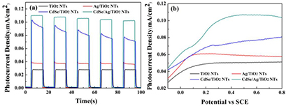
Figure 6. (a) Transient photocurrent response and (b) current density versus applied potential of all samples measured under simulated solar light irradiation in 0.5 M Na2SO4.
Download figure:
Standard image High-resolution imageIt is known that the charge transfer resistance of interfaces has a vital effect on the photoelectrochemical properties of nanocomposites [37, 38]. Electrochemical impedance spectroscopy (EIS) is a powerful tool for investigating the interfacial properties. The diameter of the semicircle represents charge transfer resistance, which is essential for photocatalytic activity (figure 7(a)) [39]. In the equivalent circuit (inset in figure 7(a)), Rs represents the resistance of the system, and Rp and CPE1 represent the resistance of semiconductor depletion layer and the capacitance, respectively [40]. The simulated values of resistance (Rp) follow the orders: TiO2 NTs (22 904 Ω) > Ag/TiO2 NT (17 160 Ω) > CdSe/TiO2 NT (9701 Ω) > CdSe/Ag/TiO2 NTs (4679 Ω). The corresponding results suggest that loading CdSe or Ag is beneficial to e−/h+ pairs separation and faster transfer. Obviously, CdSe and Ag co-sensitized TiO2 NTs further reduce the charge transfer resistance and possess a much higher charge transfer rate, which means excellent photoelectric performance. The lowest charge transfer resistance also indicates that Ag nanoparticles can enhance the conductivity of CdSe/Ag/TiO2 NTs efficiently; that may be why CdSe/Ag/TiO2 NTs possess a higher photocurrent density compared with CdSe/TiO2 NTs.
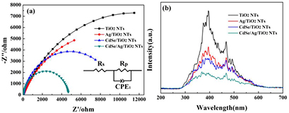
Figure 7. (a) Electrochemical impedance spectra of Nyquist plots, the inset is the equivalent circuit model; (b) PL spectra of these samples with the excitation wavelength of 220 nm at room condition.
Download figure:
Standard image High-resolution imageThe PL spectra for as-formed samples were recorded for further investigating the charge separation and recombination. Figure 7(b) displays the PL spectra of TiO2 NTs, CdSe/TiO2 NTs, Ag/TiO2 NTs and CdSe/Ag/TiO2 NTs. The pure TiO2 NTs has the highest intensity with peaks at 396 nm and 468 nm [41]. Other samples show similar peak positions under the same conditions. After the modification of Ag nanoparticles or CdSe, the PL emission intensity is obviously lower than that of TiO2 NTs, suggesting that loading Ag or CdSe could relatively induce the decrease in electron–hole pair recombination rate. CdSe/Ag/TiO2 NTs shows the weakest emission among all the samples, suggesting improved electron–hole separation.
As demonstrated in figure 8, the slopes of the tangent lines in the Mott-Schottky plots are all positive, representing the n-type nature of TiO2 [42]. Importantly, the flat band potential Efb of a semiconductor is essential to the photoelectrochemical reactions and equal to the Fermi energy under flat band conditions. The more positive the flat band potential, the greater the curvature of the semiconductor energy band, which facilitates charge carrier transfer at the semiconductor-electrolyte interface [43]. Notably, the Efb of Ag/TiO2 NTs (0.82 V) and CdSe/TiO2 NTs (1.88 V) are more positive than that of TiO2 NTs (−0.05 V) and the Efb of CdSe/Ag/TiO2 NTs (2.33 V) is the most positive. It reveals that the sample CdSe/Ag/TiO2 NTs possess the greatest energy band curvatures and the fastest interfacial carrier transfer. Combined with the results of I–t and I–V analyses, interfacial resistance can be effectively reduced and interfacial contact be greatly improved by introducing Ag NPs compared with CdSe/TiO2 NTs. It could be speculated that CdSe/Ag/TiO2 NTs possess the best photoelectric catalysis performance among those samples.
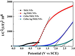
Figure 8. Mott–Schottky plots measured at a frequency of 1000 Hz of TiO2 NTs, Ag/TiO2 NTs, CdSe/TiO2 NTs and CdSe/Ag/TiO2 NTs, the bias potential is 0.5 V (versus SCE) in 0.5 M Na2SO4 aqueous solution.
Download figure:
Standard image High-resolution imageThe CdSe/Ag/TiO2 NTs excited under irradiation present extraordinary photoelectrochemical performance, which derives from their superior microstructure. In this work, Ag NPs are a key factor for enhanced photoelectrochemical performance. According to the TEM results, a special structure was established among CdSe nanocrystals, Ag nanoparticles and TiO2, which have an impact on electron transport. The changes in lifetimes (τ) measured for TiO2 NTs, Ag/TiO2 NTs, CdSe/TiO2 NTs and CdSe/Ag/TiO2 NTs can estimate their efficiency of carrier separation and suggest the carrier transmission path. As we all know, carrier separation ability and electron lifetimes are closely related to the transfer path of photo-induced electron [44]. The Bode phase plots of samples were measured under 300 W Xe lamp irradiation with 365 nm monochromatic light filter and illustrated in figure 9(a). The lifetimes of the charge carrier were calculated by the formula [45]: τ ≈ 1/(2πf) and the calculated electron lifetimes of samples were presented in figure 9(a). Remarkably, the electron lifetime of Ag/TiO2 NTs (0.243 ms) has no obvious difference to that of TiO2 NTs (0.242 ms), which indicates that Ag NPs have little effect on the charge carrier separation in the Ag/TiO2 NT system. The electron lifetime of the sample CdSe/TiO2 NTs (0.34 ms) is 1.4 times that of TiO2 NTs, resulting from the heterostructure of CdSe/TiO2 NTs [1]. Particularly, the electron lifetime of CdSe/Ag/TiO2 NTs reached 2.37 ms, which is 6.97 and 9.75 times that of CdSe/TiO2 NTs and Ag/TiO2 NTs. That demonstrates that Ag NPs as the transmission medium can greatly inhibit charge recombination and efficiently accelerate electron transfer from CdSe to TiO2.
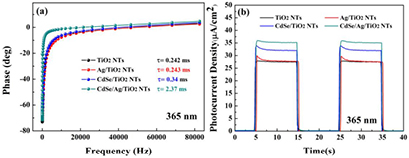
Figure 9. (a) Bode phase spectra of samples and (b) transient photocurrent response under 300 W Xe lamp irradiation with 365 nm monochromatic light filter.
Download figure:
Standard image High-resolution imageBased on the above-mentioned analyses, it can be concluded that a unique carrier-transfer-channel of excited electrons is obtained, due to the difference of conduction band energies among CdSe, Ag and TiO2 NTs with a stepwise band structure [46–48]. Figure 10 depicts the possible carrier transfer mechanism of that microscopic structure. It is well known that Ag Fermi energy level is lower than the conduction band of CdSe, resulting in rapid transfer of electrons from CdSe to Ag [20, 49]. Moreover, the Fermi level of the Ag nanoparticles will be more negative after the equilibrium for the electron accumulation, getting a new Fermi level [49]. Then, the stored electrons could inject into CB of TiO2, and transfer to the titanium substrate across a vertical nanotube, generating a higher photocurrent at 0.5 V bias (figure 10). Clearly, no obvious change of photocurrent can be seen between Ag/TiO2 NTs (27.65 µA cm−2) and TiO2 NTs (27.58 µA cm−2). However, the transient photocurrent of CdSe/Ag/TiO2 NTs (35.06 µA cm−2) is higher than that of CdSe/TiO2 NTs (31.96 µA cm−2), Ag/TiO2 NTs and TiO2 NTs (figure 9(b)), which further proves a rapid transmission channel in the ternary composite. Photocurrent enhancement of CdSe/Ag/TiO2 NTs is well in agreement with the analyses in figure 6.
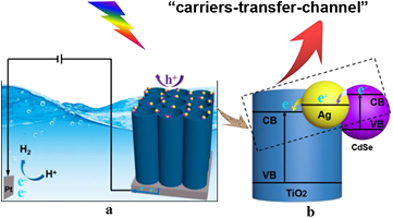
Figure 10. Schematic diagram of the charge carrier transfer of photoelectrocatalysis for CdSe/Ag/TiO2 NTs under light irradiation.
Download figure:
Standard image High-resolution imageFurthermore, the electron lifetimes of all samples are investigated under 300 W Xe lamp irradiation with a 475 nm monochromatic light filter (figure 11(a)). There is almost no change about the electron lifetime of CdSe/TiO2 NTs (0.19 ms) compared with that of TiO2 NTs (0.18 ms), because of the low transfer efficiency between CdSe and TiO2 [44]. However, the electron lifetime of Ag/TiO2 NTs (4.54 ms) is greatly enhanced, which is 25.22 times that of pure TiO2 NTs, resulting from the surface plasmon effect of Ag under irradiation [50]. Interestingly, the carrier in the CdSe/Ag/TiO2 NTs (1.9 ms) has a shorter lifetime compared with Ag/TiO2 NTs, but it is still an improvement over that of TiO2 NTs. It can be concluded that the surface plasmon effect of Ag has an important effect on photoelectric performance with excited hot electrons injecting into TiO2 (figure 11(b)). The presented results reveal that Ag NPs play a dual role in carrier transfer processes in the ternary system, leading to an improved photoelectrochemical performance compared with CdSe/TiO2 NTs. That is also well consistent with the reduced interfacial resistance and facilitates charge carrier transfer at the semiconductor-electrolyte interface.
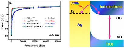
Figure 11. (a) Bode phase spectra of samples under 300 W Xe lamp irradiation with 475 nm monochromatic light filter; (b) plasmonic energy transfer from the excited Ag nanoparticles to TiO2 under the irradiation.
Download figure:
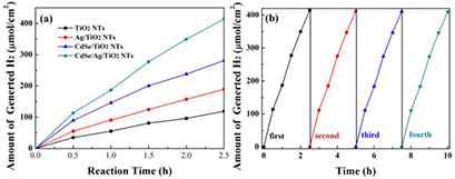
Standard image High-resolution imageThe photocatalytic activities of samples were also evaluated by the actual generated hydrogen. Figure 12(a) shows the hydrogen production yields of all the samples at the same conditions. The generated hydrogen of Ag/TiO2 NTs, CdSe/TiO2 NTs reached 189.44 µmol cm−2 and 281.42 µmol cm−2, respectively, indicating that their catalytic were improved compared with that of pure TiO2 NTs (119.29 µmol cm−2). CdSe/Ag/TiO2 NTs exhibit the highest hydrogen yield (413.99 µmol cm−2), which is better than that of Ag/TiO2 NTs and CdSe/TiO2 NTs. That was because of the synergistic effect of Ag and CdSe, which could dramatically enhance the photoelectric catalysis performance. Furthermore, the hydrogen production yields of CdSe/Ag/TiO2 NTs still can reach 410.36 µmol cm−2 after four cycle experiments (figure 12(b)), showing its excellent stability.
Figure 12. (a) Hydrogen produced rate over all samples under light irradiation; (b) cyclic H2 production curves for the CdSe/Ag/TiO2 NTs.
Download figure:
Standard image High-resolution image
4. Conclusion
Ag nanoparticles and CdSe nanocrystals were successively loaded on the surface of TiO2 nanotube arrays via microwave assisted chemical reduction and in situ fabrication methods. Ag nanoparticles with dual roles can significantly enhance the photoelectrochemical performance of ternary composite. CdSe/Ag/TiO2 NTs exhibit excellent light absorption properties and the introduction of Ag can reduce the charge transfer resistance between CdSe and TiO2. CdSe/Ag/TiO2 NTs possess the highest hydrogen production yield of 413.99 µmol cm−2 after 2.5 h, exhibiting optimal photoelectric catalytic activity.
Acknowledgments
This work was supported by the National Natural Science Foundation of China (Nos. 21676213, 21476183, and 51372201), the China Postdoctoral Science Foundation (No. 2016M600809), and the Natural Science Basic Research Plan in Shaanxi Province of China (Nos. 2017JM2026 and 2014JM2-2012).