
Abstract
We present a comparative study of the C-face and Si-face of 3C-SiC(111) grown on off-oriented 4H-SiC substrates by the sublimation epitaxy. By the lateral enlargement method, we demonstrate that the high-quality bulk-like C-face 3C-SiC with thickness of ~1 mm can be grown over a large single domain without double positioning boundaries (DPBs), which are known to have a strongly negative impact on the electronic properties of the material. Moreover, the C-face sample exhibits a smoother surface with one unit cell height steps while the surface of the Si-face sample exhibits steps twice as high as on the C-face due to step-bunching. High-resolution XRD and low temperature photoluminescence measurements show that C-face 3C-SiC can reach the same high crystalline quality as the Si-face 3C-SiC. Furthermore, cross-section studies of the C- and Si-face 3C-SiC demonstrate that in both cases an initial homoepitaxial 4H-SiC layer followed by a polytype transition layer are formed prior to the formation and lateral expansion of 3C-SiC layer. However, the transition layer in the C-face sample is extending along the step-flow direction less than that on the Si-face sample, giving rise to a more fairly consistent crystalline quality 3C-SiC epilayer over the whole sample compared to the Si-face 3C-SiC where more defects appeared on the surface at the edge. This facilitates the lateral enlargement of 3C-SiC growth on hexagonal SiC substrates.
Export citation and abstract BibTeX RIS

Original content from this work may be used under the terms of the Creative Commons Attribution 3.0 licence. Any further distribution of this work must maintain attribution to the author(s) and the title of the work, journal citation and DOI.
Introduction
Silicon carbide (SiC) exhibits a range of favorable physical, mechanical and electronic properties making it attractive as an alternative material for next-generation electronic devices [1, 2]. Among the different SiC polytypes, cubic silicon carbide (3C-SiC) with a bandgap of 2.36 eV has prominent physical properties including high electron mobility, drift velocity and low interface trap density compared to other SiC polytypes and conventional semiconductors [3, 4]. In recent years, 3C-SiC is increasingly considered as an attractive material for the development of various semiconductor applications such as biosensors, photovoltaic devices, as well as solar-driven water splitting [5–7]. It is also an appropriate substrate for the growth of graphene, especially, multilayer graphene [8, 9].
The SiC exhibits two polar faces that are referred to Si-face and C-face for (0001) and (0 0 0  ) in hexagonal SiC and (1 1 1) and (

 ) in cubic SiC respectively. In case of hexagonal polytypes, there exist works reporting reduction of the interface trap density (Dit) by changing the crystal polarity [10, 11], thereby improving the channel mobility of SiC MOSFETs. A lower value of Dit on C-face of hexagonal SiC could be achieved using H2 annealing [12], which reveals the potential of C-face for improving the performance of SiC devices. In addition, the C-face SiC attracts much attention for the growth of graphene because the electronic band structure of the epitaxial graphene grown on C-face SiC is quite different from that on Si-face [13–15]. For instance, it is reported that the graphene grown on the C-face 4H-SiC shows higher electric carrier transport parameters than that on the Si-face at room temperature [16]. In case of the cubic polytype, the C-face 3C-SiC grown on hexagonal SiC substrate has shown additional superiorities compared to the Si-face 3C-SiC. A two-dimensional electron gas (2DEG) was observed in C-face 3C-SiC/6H-SiC heterostructures due to their conduction band offset and the positive polarization charge on the C-face 6H-SiC [17]. The authors also reported quantum confinement and coherence in the 2DEG in the C-face 3C-SiC/6H-SiC [18], which makes this heterostructure a promising candidate for high electron mobility transistors. Moreover, the C-face 3C-SiC could also be a promising substrate for the graphene growth. So far, most studies reported the growth of 3C-SiC on Si-face of hexagonal SiC substrates and there are only few reports on the growth of C-face 3C-SiC [19–22].
Nominally on-axis hexagonal SiC substrates have been commonly used for the growth of 3C-SiC layers. In this case, the 3C-SiC spontaneously nucleates in a 2D mode all over the surface [22, 23]. Consequently, a high density of structural defects called double positioning boundaries (DPBs) are formed [21]. The DPB is recognized as a fundamental problem that hinders 3C-SiC development and it is attributed to the fact that 3C-SiC has two types of stacking sequence with a 60° rotation variation (i.e. ABC and ACB). Many studies have focused on the reduction of DPBs via optimizing some parameters such as source-gas concentration, surface etching, C/Si ratio, and temperature [24, 25]. However, the achievements have been marginal in terms of reproducibility.
Recently, it has been demonstrated that DPBs can be significantly reduced and even a single domain 3C-SiC can be grown by a lateral enlargement (LE) mechanism on off-oriented hexagonal Si-face SiC substrates via the sublimation epitaxy [26, 27]. So far, this new concept using off-oriented hexagonal Si-face SiC as a substrate has been used for the growth of high-quality Si-face 3C-SiC. However, the growth of C-face 3C-SiC on off-oriented hexagonal SiC substrate has not been explored. In this work, we study comparatively the 3C-SiC grown on C-face and Si-face of 4 degree off-oriented 4H-SiC substrates and demonstrate that high-quality DPB-free 3C-SiC with thickness up to ~1 mm can be grown on C-face of hexagonal SiC substrates using sublimation epitaxy.
Experimental
The sublimation growth system consists of a growth chamber with a closed graphite crucible, which is heated by induction, as previously reported [26]. Inside the graphite crucible a polycrystalline SiC plate is placed onto a tantalum (Ta) foil followed by a 1 mm thick graphite spacer with a circular opening (7 mm in diameter). The Ta foil is used as a carbon getter in order to create a silicon-rich atmosphere which is preferable for the formation of 3C-SiC. A 4° off-oriented (0 0 0 1) 4H-SiC substrate was put on the top of the spacer with either the Si- or the C-face facing the polycrystalline SiC source. Before the growth, all 4° off-oriented 4H-SiC substrates were chemically cleaned by acetone, ethanol, H2O: NH3: H2O2 (5:1:1) and H2O: HCl: H2O2 (6:1:1). The crucible was heated up to 1900 °C with a ramping rate of 30 °C min−1, and then kept at a constant growth temperature for 2 h after which it was cooled down to the room temperature. Under such growth conditions, the growth rate of the epilayer was about ~450 µm h−1. All of the experiments were done in vacuum (10−5 mbar).
The surface topography was investigated using Nomarski optical microscope and atomic force microscope (AFM) in tapping mode. Low-temperature photoluminescence (LTPL) spectra were measured at 2 K using the 351 nm line of an Ar+-ion laser for excitation. The laser-spot diameter on the sample was about 100 µm. The spectra were recorded using a monochromator equipped with a 1200 grooves mm−1 grating in combination with a CCD camera. The resulting spectral resolution is about 1 Å. The crystalline quality of the grown material was measured by high-resolution x-ray diffraction (HRXRD) ω rocking curve utilizing diffractometer operating in a triple axis mode equipped with Cu Kα1 anode at 45 KV and 40 mA, 2-bounce Ge(2 2 0) hybrid monochromator as well as 3-bounce Ge(2 2 0) symmetrical analyzer. Raman spectra were obtained using a micro-Raman setup with 532-nm laser line excitation. The laser beam was focused on samples through a 100 × microscope objective to a spot of diameter ~0.8 µm. The laser power was about 17 mW measured before the objective. The spectra were detected using a monochromator with 600 grooves mm−1 grating coupled to a CCD camera, resulting in spectral resolution of ~5.5 cm−1.
Results and discussion
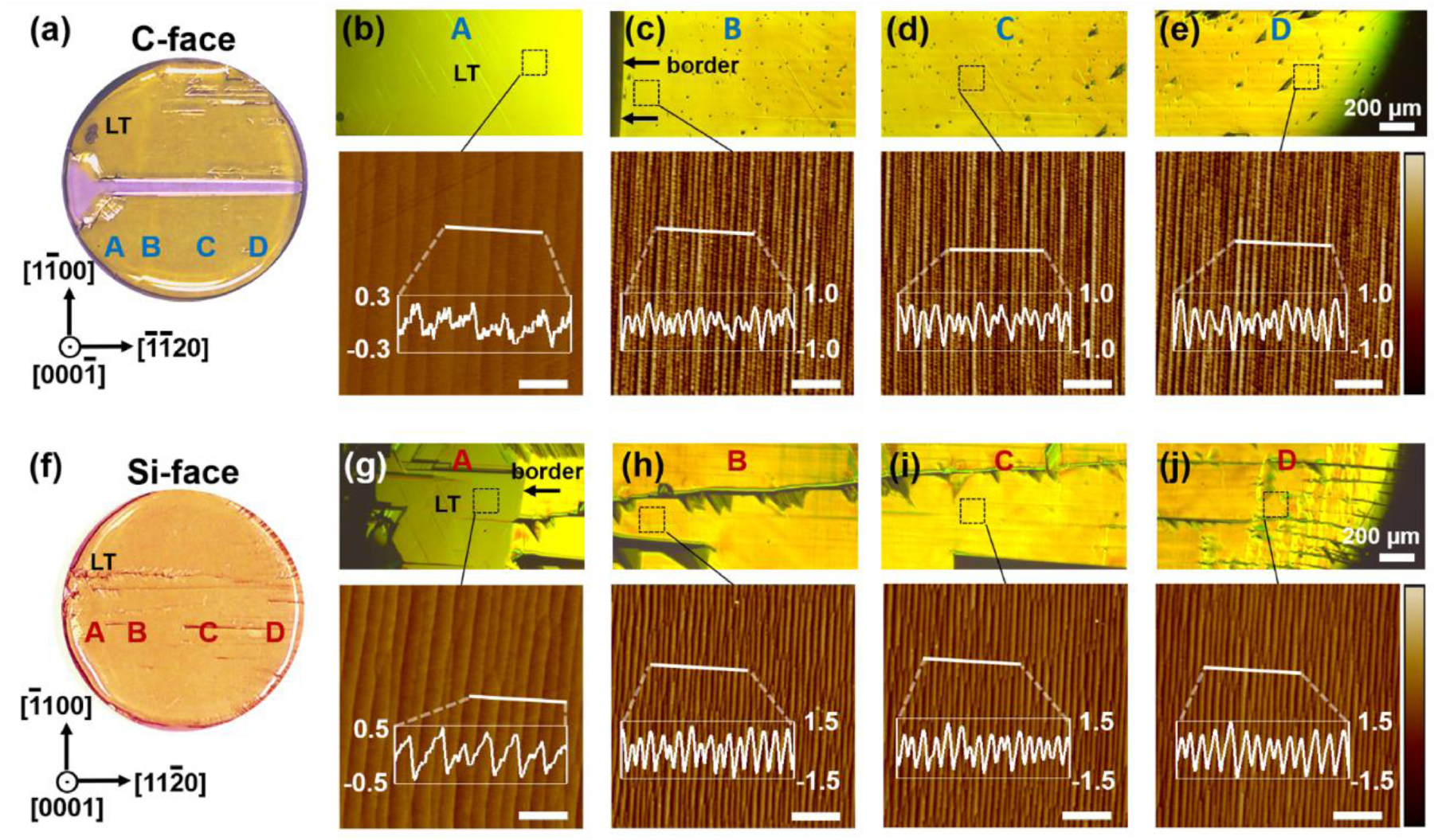
Overview pictures of typical 900 µm thick free-standing (substrates were removed by mechanical polishing) C-face and Si-face 3C-SiC samples are shown in figures 1(a) and (f), respectively. The growth of 3C-SiC on C- and Si-face 4H-SiC substrates with 4 degrees off-orientation proceeds in a similar manner. In both case the 3C-SiC starts to nucleate at the edge of the sample on a facet or a large terrace (LT) with an on-axis surface and later laterally enlarges along the step-flow direction. Detailed description of 3C-SiC growth mechanism on off-oriented 4H-SiC (0 0 0 1) substrates can be found in previous report [26].

Figure 1. (a) An overview of the 900 µm thick free-standing C-face 3C-SiC with a diameter of 7 mm. (b)–(e) Optical microscopy images of the C-face 3C-SiC collected at the location A on the large terrace (b), at the location B close to the large terrace border (c), at the location C at the center of the sample (d), and at the location D at the edge (e). (f) An overview of the 900 µm thick free-standing Si-face 3C-SiC with a diameter of 7 mm. (g)–(j) Optical microscopy images of the C-face 3C-SiC collected at the location A on the large terrace (g), at the location B closed to the large terrace border (h), at the location C at the center of the surface (i), and at the location D at the edge (j). The location of the 2 × 2 µm2 AFM topography images are indicated by the black squares in the optical micrographs. The inset in AFM images show the periodic step arrangement. Scale bars in optical micrographs and AFM images are 200 µm and 400 nm, respectively. Color scales of AFM images are ±1.0 nm for the C-face and ±1.5 nm for the Si-face.
Download figure:
Standard image High-resolution imageIn order to investigate the evolution of the surface morphology from the large terrace to the opposite edge of the sample along the step-flow direction, optical micrographs were taken along this path at the large terrace (LT, point A), close to the large terrace (point B), at the center of the path (point C), and at the edge opposite to the large terrace (point D).
Macroscopically we observe two differences between the C- and Si-face 3C-SiC samples. At the large terrace areas (point A), the C-face sample has a 4H-SiC polytype inclusion that extends all the way to the opposite side. The Si-face sample is free of polytype inclusions as observed by naked eye or in optical microscopy, while we could observe a few DPBs. In general, we observed experimentally that 3C-SiC polytype stability on off-oriented 4H-SiC ( ) is lower compared to 4H-SiC (0 0 0 1). This could be related to the differences in surfaces energies of polar faces of hexagonal SiC substrate which influences the initial 3C-SiC formation [20].
The microscopic difference between C- and Si-face 3C-SiC is in the surface steps structure. The AFM images were acquired from locations denoted by black squares in the corresponding optical micrographs. It can be observed in figure 1(b) that the C-face 3C-SiC laterally grows along the [ ] direction by the step-flow growth mode, which is similar to the Si-face 3C-SiC growth reported in the previous work [26]. The AFM image taken on the C-face 3C-SiC domain on the LT shows periodic steps with wide terraces of 150–200 nm and step height of 0.25–0.5 nm. The arrows in figure 1(c) indicate the border of the LT. At distance from the LT, the AFM images collected at different locations (B, C, D) further away along the step-flow direction of the C-face 3C-SiC show narrower and highly periodic steps with a step height of ~0.75 nm and terrace width of ~50 nm. The statistical data shown as histogram (figure 2(a)) of step heights on the C-face 3C-SiC confirms that most of the steps are distributed around 0.75 nm height, which corresponds to three Si-C bilayers or one-3C-SiC unit cell. The AFM images measured on these positions (B, C, and D) do not exhibit obvious variation (figures 1(c)–(e)), indicating that no other nucleation sites form on the step-flow propagation path. Otherwise, newly formed nucleation sites would impede the step-flow growth and form DPBs. The AFM reveals surface roughness (Rq) of approximately ~0.37 nm.

Figure 2. Statistic histograms of the step heights for (a) the C-face and (b) the Si-face 3C-SiC, respectively. The step heights are obtained from several AFM topography images of each sample.
Download figure:
Standard image High-resolution imageIn comparison, the AFM of Si-face 3C-SiC sample shows periodic steps with wide terraces of 120–200 nm and step height of 0.5–0.75 nm at the LT (figure 1(g)). As shown in figures 1(h)–(j), the AFM images measured on locations B-D exhibit homogeneously distributed steps with a height of ~1.5 nm and terrace width of ~55 nm. The statistical data is shown as histogram in figure 2(b) and confirms that most of the steps are distributed around 1.5 nm, which corresponds to six Si-C bilayers (two 3C-SiC unit cells). The Si-face sample exhibits steps twice as high as on the C-face due to the step-bunching. Consequently, the surface roughness (Rq) carried out from the Si-face images is approximately ~0.65 nm, which is larger than the value of ~0.37 nm obtained for the C-face.
At the opposite edge (point D), the C-face 3C-SiC exhibits a smooth surface at the edge (figure 1(e)) while the Si-face 3C-SiC shows a rather rough surface with a lot of cracks near the edge (figure 1(j)) and corrugated features aligned along the [ ] direction can be observed as well. The range for the up and down fluctuations of these corrugations was not possible to disclose using AFM and could be several micrometers. A possible reason for the difference in 3C-SiC morphology on Si-face and on C-face is discussed below in respect to the polytype transition from 4H to 3C-SiC.
In addition, there is a difference in step structure along the [ ] direction on C- and Si-face 3C-SiC surfaces. On the C-face, the steps are straight and have perturbation in straight in tens or even hundreds of micrometers. In contrast, the steps on the Si-face 3C-SiC show overlapping features with separation of only 1–2 µm. The overlapping features also indicate that the step-bunching is more pronounced on the Si-face 3C-SiC surface. The same tendency of step-bunching formation was also observed on polar faces of 6H- and 4H-SiC epilayers grown by chemical vapor deposition [28]. The surface free energy on the Si-face is higher than that on the C-face [29]. Hence, the mechanism of surface energy minimization on the Si-face is more complex and could be a possible reason for the step-bunching and step structure instabilities formation.
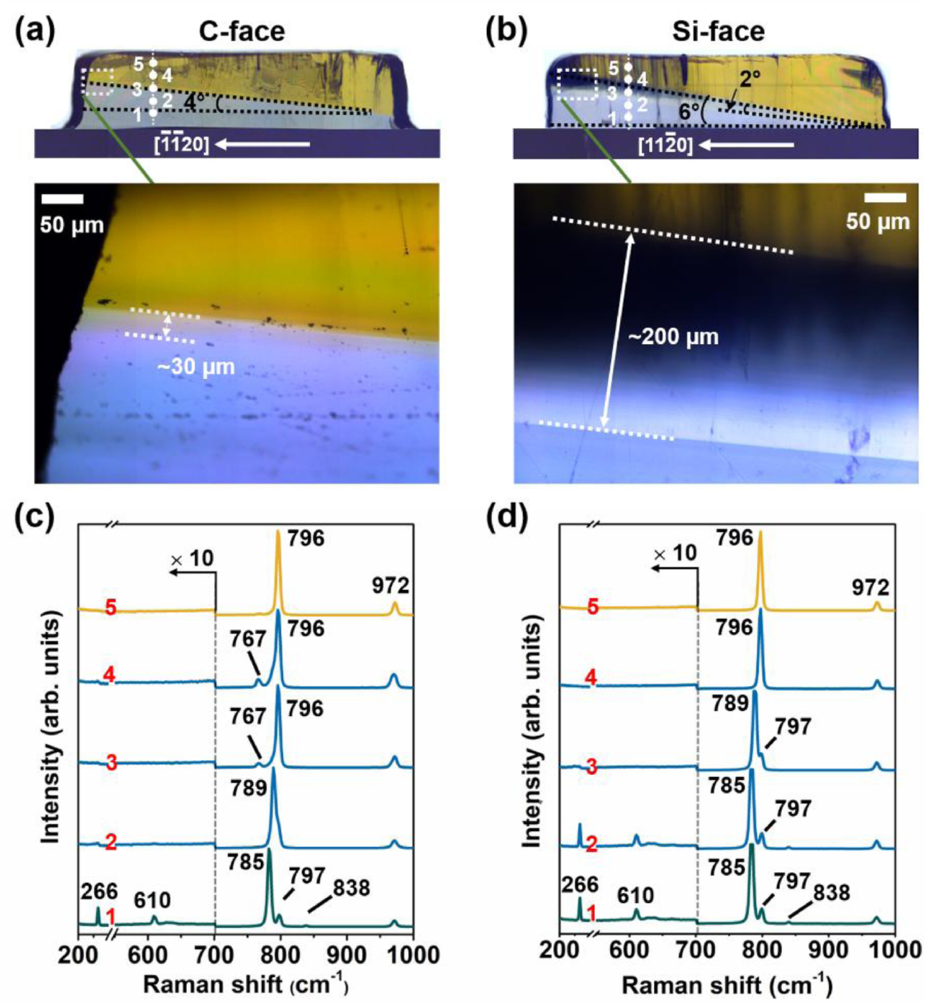
Figure 3 compares the cross-sectional optical microscope images of the C-face and the Si-face 3C-SiC samples. The thicknesses of both Si- and C-face SiC layers are approximately 900 µm. As reported previously [26], the growth of 3C-SiC layer on off-oriented 4H-SiC can be viewed as a three-layer system, where a homoepitaxial 4H-SiC layer is first formed on the substrate, followed by the formation of a transition layer and subsequently 3C-SiC layer on the top. In both, the C-face and the Si-face 3C-SiC samples, we observe the homoepitaxial 4H-SiC layer and the transition layer between the 3C-SiC and the 4H-SiC substrate, as shown in figures 3(a) and (b). Interestingly, the tilt angle between the substrate and the 3C-SiC epilayer is approximately 4° in the C-face sample and 6° in the Si-face sample. A tilt angle between the substrate and the Si-face 3C-SiC almost two times larger than the off-cut angle was reported in previous work [26]. Therefore, a tilt angle similar to the off-cut angle of the substrate in the C-face 3C-SiC sample indicates that the 3C-SiC layer development on the C-face of 4 degrees off-oriented 4H-SiC substrates is different. This is supported by analyzing the cross-sectional images of the C- and Si-face 3C-SiC samples. As seen in figures 3(a) and (b), at the edges on the left side of cross-sectional images, indicated by the white squares, the thickness of the transition layer in the C-face sample is around 30 µm while it is around 200 µm in the Si-face 3C-SiC sample. This thickness difference could be explained by the following. Due to the step-bunching phenomena, the step height in the homoepitaxial 4H-SiC layer grown on the Si-face substrate might be larger than that grown on the C-face substrate [28]. The complexity of transition is further increased by the step-bunching of 3C-SiC and overlapping features. Consequently, the larger step height would result in a larger angle of the transition layer when it is propagated along the step-flow direction. As discussed above, we observed that the step height of Si-face 3C-SiC is twice higher than that on the C-face. Furthermore, various structural defects are expected to form within the transition layer and propagate through the 3C-SiC layer, especially at the edge where the transition is very thick, as observed in figure 3(b). It has been reported that the extended defects within the 3C-SiC domain originate from the hetero-interface [30]. To some extent, the generated defects within the transition layer contributes to defects observed on the surface at the edge of the sample (point D in figure 1(j)) with corrugation features. Therefore, a more direct transition of C-face growth is beneficial for a more fairly consistent crystalline quality 3C-SiC epilayer over the whole sample, thus facilitating the LE of 3C-SiC growth on hexagonal SiC substrates. This explains why we observe more defects on the surface at the edge of the Si-face 3C-SiC than that at the edge of the C-face 3C-SiC (see a comparison of figures 1(e) and (j)).
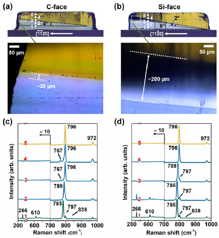
Figure 3. (a) and (b) Optical microscope images of the cross-sectional view of (a) the C-face and (b) the Si-face 3C-SiC samples. The total thickness of both samples is approximately 900 µm. The lower panels show enlarged optical micrographs magnified near the edge of the samples focusing on the transition layers, as indicated by white squares. (c) and (d) Micro-Raman spectra measured on points along the white dashed line on the cross-sectional pieces in (a) and (b), respectively. Note that Raman spectra are magnified ten times in the range of 200–700 cm−1.
Download figure:
Standard image High-resolution imageMicro-Raman spectroscopy was used to characterize the polytypes of the transition layers in both C- and Si-face 3C-SiC samples. Two scan lines were measured from the bottom to the top on both cross-sectional pieces with a spot diameter (lateral resolution) below 1 µm and a step size of 100 µm, as indicated in figures 3(a) and (b). Five Raman spectra chosen from the scan line on each sample are presented in figures 3(c) and (d), respectively. For the C-face sample shown in figure 3(c), the Raman spectrum of point 1 shows several peaks at 266, 610, 785, 797, and 838 cm−1, which correspond to different Raman modes of 4H-SiC [31, 32]. This confirms the formation of 4H-SiC homoepitaxial layer. The line appearing at 789 cm−1 for point 2 corresponds to the folded TO (FTO) mode of 6H-SiC. A weak peak located at 767 cm−1 can be observed in points 4 and 5, which is attributed to contribution from the FTO mode of 6H-SiC. This indicates that the transition layer contains (at least) inclusions of 6H-SiC polytype, but formation of other polytypes on a microscopic level cannot be precluded. The peaks at 796 cm−1 and 972 cm−1, corresponding to the FTO and FLO modes of 3C-SiC, gradually dominate the spectra for points 3, 4, and 5. At the same time, the folded modes associated with hexagonal polytypes (266, 610, 767, 785, 789, and 838 cm−1) vanish at points 4 and 5. This clearly confirms the formation of 3C-SiC on top of the transition layer. Similar evolution trend is observed from the cross-sectional piece of the Si-face 3C-SiC, as seen in figure 3(d). Point 1 exhibits the typical Raman spectrum of 4H-SiC homoepitaxial layer. Again, a sharp peak at 789 cm−1 in combination with a weak peak at 797 cm−1 are observed for point 3, which may correspond to 6H-SiC. The modes of 3C-SiC at 796 cm−1 and 972 cm−1 dominate the spectra for points 4 and 5. Thus, the Raman results confirm the formation of the 4H-SiC homoepitaxial layer and transition layer prior to the growth of 3C-SiC on both C- and Si-face off-oriented 4H-SiC substrates and evidence the more direct polytype conversion observed in the C-face sample.
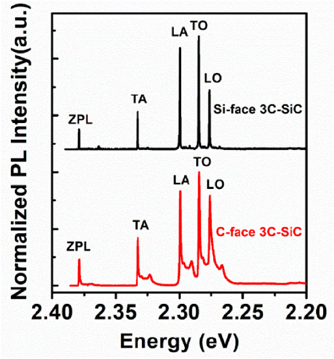
To characterize the optical properties of 3C-SiC, we carried out LTPL measurements at 2 K on both C- and Si-face 3C-SiC samples, which is a well-known tool to indicate the quality. Typical spectra of the C- and Si-face 3C-SiC are shown in figure 4. Both spectra exhibit well-resolved nitrogen-bound-exciton zero-phonon line (ZPL) accompanied with its four momentum-conserving phonon replicas (denoted as TA, LA, TO, and LO) [33]. The width (FWHM) of the TA-phonon line can be used to estimate the nitrogen doping concentration of 3C-SiC [34]. The FWHM values of the TA lines in both C- and Si-face 3C-SiC are around 1 meV, which corresponds to nitrogen doping concentration of around 1 × 1016 cm−3 [34]. This indicates that the choice of the polar face of the SiC substrate does not affect substantially the nitrogen background (unintentional) doping in the 3C-SiC during the sublimation growth. Furthermore, the intensity ratio of LA to TO phonon replicas (ILA/ITO) can be used to evaluate the biaxial stress, as suggested previously [35]. The typical value of ILA/ITO is around ~0.19 in 3C-SiC thin films grown on Si substrates, and reflects that the film is subject to substantial tensile stress [35]. In our case, the ratio ILA/ITO is around 0.8 for both the C- and Si-face 3C-SiC samples, indicating much less (presumably negligible) residual stress. This may be expected since it is a SiC system with hexagonal to cubic transformation in comparison to Si to SiC system.
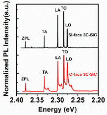
Figure 4. Normalized (to the TO peak) LTPL spectra of Si- and C-face 3C-SiC grown on 4 degree off-oriented 4H-SiC substrates.
Download figure:
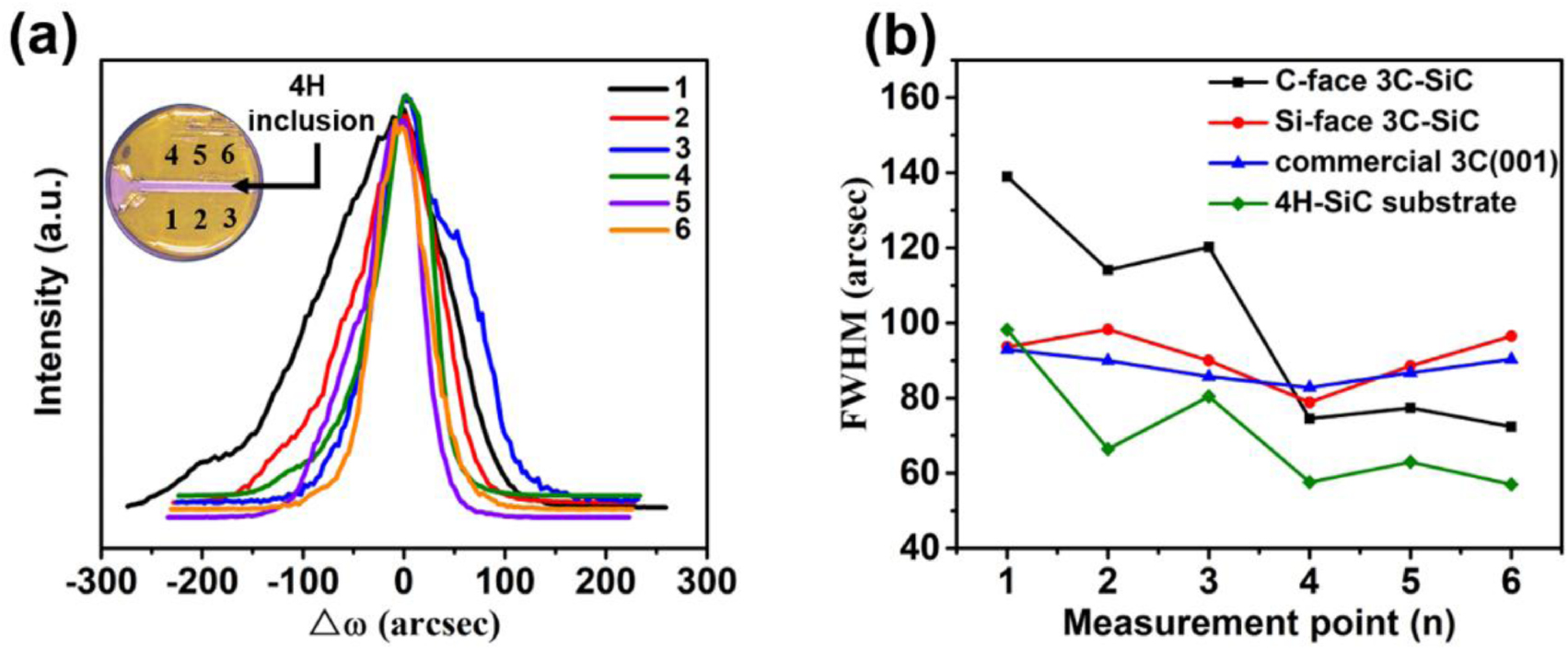
Standard image High-resolution imageTo study the crystalline quality of the C- and Si-face 3C-SiC, HRXRD (1 1 1) ω-rocking curve measurements were performed with a footprint of 1 × 2 mm2. Figure 5(a) shows HRXRD (1 1 1) ω-rocking curves measured at six points over the C-face 3C-SiC sample with a step of 2 mm (three points on each 3C-SiC domain, see inset in figure 5(a)). These ω-rocking curves show full width at half-maximum (FWHM) of 139, 114, 120, 74, 77, and 72 arcsec at the different locations. Points 4, 5, and 6 exhibit very sharp peaks with FWHM values of 70–80 arcsec, suggesting a higher crystalline quality on this 3C-SiC domain (above the 4H-SiC inclusion, see the inset in figure 5(a)) compared to the one below the 4H-SiC inclusion. This divergence is likely formed at the stage of initial nucleation on the large terrace. As a comparison, the HRXRD (1 1 1) ω-rocking measurements on the Si-face 3C-SiC(1 1 1) sample, commercial 3C-SiC(0 0 1) and Si-face 4H-SiC(0 0 0 1) substrates were also carried out using the same measurement configuration. The commercial 3C-SiC(0 0 1) and 4H-SiC(0 0 0 1) substrates have average FWHM values of 80–100 and 60–80 arcsec, respectively. As seen in figure 5(b), the FWHM values of the C-face 3C-SiC sample are comparable to the ones of the Si-face 4H-SiC(0 0 0 1) substrates. To the best of our knowledge, this is the first report that the C-face 3C-SiC has such a high crystalline quality over a large single domain [20].

Figure 5. (a) HRXRD ω-rocking curve collected from (1 1 1) Bragg reflection for the C-face 3C-SiC sample. The inset indicates the measurement points. (b) FWHM values on different measurement points of the C- and Si-face 3C-SiC in comparison with commercial 4H-SiC and 3C-SiC(0 0 1) samples.
Download figure:
Standard image High-resolution imageIn addition, the HRXRD rocking curve for the C-face 3C-SiC epilayer grown on nominally on-axis 6H-SiC reported in the literature consists of several overlapped peaks and shows a FWHM value of few hundred arcsec [20]. These overlapped peaks are generated from many sub-domains, which are slightly tilted with respect to each other at very small angles. The sub-domains are typically observed in the case of epitaxial growth of 3C-SiC on nominally on-axis 4H- or 6H-substrates [36]. In contrast, sub-domains do not exist in our samples, which demonstrates the superiority of the off-axis transformation compared to the on-axis one.
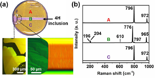
As mentioned above, the C-face 3C-SiC sample contains a narrow stripe representing a 4H-SiC inclusion. Figure 6(a) depicts the magnified optical microscope images of the 4H-SiC inclusion in the C-face sample measured on the large terrace and near the edge of the large terrace. The 4H-SiC appearing at the large terrace clearly shows hexagonal structures associated with spiral-growth mode of 4H-SiC. As expected, the down-step part of the long narrow 4H-SiC inclusion shows a step-structured surface. This indicates that the 4H-SiC domain nucleates on the terrace and propagates by the step-flow growth mode along the [ ] direction and forms the long narrow 4H-SiC inclusion. The Raman results shown in figure 6(b) confirm that the inclusion is 4H-SiC. We believe that such a 4H-SiC inclusion can be eliminated by controlling the growth conditions properly in order to suppress the nucleation of 4H-SiC on the terrace.
Figure 6. (a) Optical microscope images of the C-face 3C-SiC sample. The magnified images show a spiral growth of 4H-SiC on the large terrace and the surface morphology of the 4H-SiC inclusion near the edge of the large terrace. (b) Raman spectra measured on three domains of the C-face sample.
Download figure:
Standard image High-resolution image
Conclusions
The growth of C-face 3C-SiC has been demonstrated on 4 degrees off-oriented C-face 4H-SiC(0 0 0 1) substrates using the sublimation epitaxy technique. AFM results show that the C-face sample exhibits a smoother surface with unit cell steps compared to the surface of the Si-face sample, which exhibits twice higher steps due to the more pronounced step bunching mechanism. As demonstrated by LTPL and HRXRD measurements, C-face 3C-SiC domains exhibit high crystalline quality similar to the Si-face 3C-SiC. Furthermore, the cross-section studies of the C- and Si-face 3C-SiC demonstrate that in both cases, a homoepitaxial 4H-SiC layer and a polytype transition layer are formed prior to the growth of 3C-SiC. However, the transition layer in the C-face sample is less complex compared with the Si-face sample. A more direct transition of C-face growth results in a more fairly consistent crystalline quality 3C-SiC epilayer over the whole sample compared to the Si-face case where we observe more defects on the surface at the edge. This facilitates the LE of 3C-SiC growth on hexagonal SiC substrates.
Acknowledgments
This work was supported by The Swedish Research Council (Vetenskapsrådet, Grant No. 621-2014-5461; 2018-04670; 2016-05362; 621-2014-5825), The Swedish Research Council for Environment, Agricultural Sciences and Spatial Planning (FORMAS, Grant No. 2016-00559), The Swedish Foundation for International Cooperation in Research and Higher Education (STINT, Grant No. CH2016-6722), The ÅForsk foundation (Grant No. 16-399), and The Stiftelsen Olle Engkvist Byggmästare (Grant No. 189-0243). V J, G R Y, R Y and M S acknowledge the financial support of the EU project CHALLENGE (project ID: 720827).
Notes
The authors declare no competing financial interest.