

Abstract
In this paper, we used tannic acid (TA) functionalized carbon nanotubes (TCNTs), and silver nanowires (AgNWs) to construct a new type of transparent conductive film (TCF) with a double-layered conductive network structure. The hybrid film exhibits excellent light transmittance, high electrical conductivity, ultra-flexibility, and strong adhesion. These outstanding performances benefit from the filling and adhesion of hydrophilic TCNT layers to the AgNW networks. Besides, we introduced the post-treatment process of mechanical pressing and covering polymer conductive polymer PEDOT:PSS, which obtained three layers of TCNT/AgNW/PEDOT hybrid film and greatly improved the comprehensive properties. The hybrid film can reach a sheet resistance of 9.2 Ω sq−1 with a transmittance of 83.4% at 550 nm wavelength, and a low root mean square (RMS) roughness (approximately 3.8 nm). After 10 000 bends and tape testing, the conductivity and transmittance of the hybrid film remain stable. The resistance of the film has no significant degradation after 14 d of exposure to high temperature of 85 °C and humidity of 85%, indicating excellent stability. The organic light-emitting diodes (OLEDs) with TCNT/AgNW/PEDOT hybrid film as anode exhibit high current density and luminosity, confirming this process has considerable potential application in photovoltaic devices.
Export citation and abstract BibTeX RIS
1. Introduction
In recent years, with the increasing market demand for new flexible optoelectronic devices such as flexible organic light-emitting diodes (OLEDs) [1–3], flexible solar cell [4], flexible touch screens [5], stretchable electronic devices [6–9], and wearable electrodes [10], flexible transparent conductive films (FTCFs) have attracted much attention as an essential part of these optoelectronic devices. Indium tin oxide (ITO), as a traditional transparent conductive material, has been widely used in solar cells and OLEDs. However, ITO cannot meet the market demand of FTCFs due to the scarcity of supply and the brittle nature of ceramics, so its application in flexible electronic devices is limited [11–14]. Hence, novel transparent conductive materials such as conductive polymers [9], carbon nanotubes (CNTs) [15], graphene [16] as well as metal nanowires [8, 10, 17–22] have attracted significant attention. Carbon-based nanomaterials have high electrical conductivity, good flexibility and stretchability, but their transparency is insufficient compared to ITO, so their excellent electrical conductivity must be sacrificed to achieve proper transparency [23].
Among these materials, silver nanowires (AgNWs), as the representative of metal nanowires, have been widely used in transparent electrodes because of their high electronic density, excellent conductivity, and high transmittance in visible light [24, 25]. However, the freshly prepared AgNW films have many insulation openings with an area of tens to hundreds of square microns. The existence of these micrometer-sized openings not only increases the series resistance for devices that rely on vertical current transmission (such as LED and solar cell) [26], but also has an impact on the continuous conductivity of other photoelectric devices, which is easy to cause partial open circuit [27]. In addition, due to the weak van der Waals force and the small contact area between the silver nanowire and the substrate, the AgNW film has low adhesion. The AgNWs are easily separated from the substrate under the action of mechanical external force [28]. These defects limit the application of AgNW film in flexible optoelectronic devices. To solve these problems, Lee et al [29] proposed a CNT-AgNW hybrid film structure. CNT can improve the hybrid film's conductivity by filling the inter-nanowire opening space of AgNW mesh to provide local electron paths. Besides, the high elastic CNT makes the hybrid network to show excellent flexibility and stretchability. However, this film-forming methods by vacuum filtration and film transfer are not conducive to large-scale production and utilization because of its complicated operation. The spin-coating method provides an ideal preparation method for constructing CNT-AgNW structure due to its simple operation and easily scalable manufacturing. Nevertheless, the hydrophobic SWCNT substrate layer severely limits the effective spin-deposition of AgNW, resulting in waste of a large amount of expensive AgNWs and seriously agglomerated. In this study, we have designed a new method and introduced phenolic hydroxyl-rich tannic acid as the basic material to modify SWCNT, and the highly hydrophilic TCNT obtained significantly facilitated the deposition of AgNWs.
Low roughness is another crucial factor for transparent conductive films to satisfy the requirements of flexible optoelectronic devices. For pure AgNW films, the raised junctions in the network worsen the roughness of the films, which is easy to cause short circuit of the photoelectric devices [30, 31]. Therefore, much effort has been devoted to achieving low roughness of AgNW films by film transfer method [32], polymer encapsulation [25, 33], mechanical pressing [10, 17, 27], but these methods sacrifice the excellent conductive properties of the original films. In this paper, we combined the post-processing method of mechanical pressing with over-covering PEDOT:PSS encapsulated the welded TCNT/AgNW network in PEDOT:PSS layer and constructed a three-dimensional conductive structure. Such a uniform and compact structure enable TCFs to maintain high conductivity and high mechanical stability under low roughness.
In this work, we provide a material saving and highly useful processing method, designed a new type of TCNT/AgNW/PEDOT TCFs, which exhibit excellent conductive performance, low roughness, ultra-flexibility, high adhesion, and excellent chemical corrosion resistance. Finally, it has been successfully applied to the flexible OLED devices, showing excellent luminous effect.
2. Experimental
2.1. Materials
High purity single-walled CNTs (SWCNTs, purity of 95 wt%, diameter less than 2 nm, length >5 μm) were provided from Carbon Star Technology (Tianjin) Co., Ltd. Sodium dodecylbenzene sulfonate (SDBS), Sodium chloride (NaCl), sodium bromide (NaBr), Tannic acid (TA), silver nitrate (AgNO3), and nitric acid (HNO3) were purchased from Aladdin. PEDOT:PSS solution (Clevios pH 1000; 1.3 wt%) was purchased from H. C. Starck. Poly(vinylpyrrolidone) (PVP; MW = 1 300 000) was purchased from Shanghai Mackin Blochemical Co., Ltd. Dimethyl sulfoxide (DMSO) was purchased from Tianjin Komio Chemical Reagent Co., Ltd. All reagents were used as received. The polyethylene terephthalate (PET) was provided from Tianjin Wanhua Co., Ltd, China with an average thickness of 150 μm. The commercial ITO-PET film was provided from south China Science & Technology Co., Ltd. Poly(N-vinylcarbazoled) (PVK) (PLT302011), N, N'-diphenyl-N, N'-bis(3-methylphenyl)- [1,1'-biphenyl]-4,4'diamine (TPD) (PTL102011B), and 8-Hydroxyquinoline aluminum (Alq3) (PLT401011G) were purchased from Xi'an Baolaite Optoelectronics Technology Co., Ltd. Lithium fluoride (LiF) and aluminum (Al) were purchased from Aladdin, and the purity was greater than 99.9%.
2.2. Synthesis of AgNWs
Silver nanowires (diameter: 50 ± 10 nm; length: 60 ± 10 μm) were prepared by the modified Li's polyol method [21]. The specific experimental details are as follows. First, four kinds of ethylene glycol solutions were prepared: (A) 110 mM NaBr, (B) 210 mM NaCl, (C) 505 mM PVP (Mw = 1 300 000), and (D) 265 mM AgNO3. After that, 23.1 ml of ethylene glycol was added to the flask, and then stirred and separately added 0.3 ml A solution and 0.6 ml B solution dropwise. After stirring for 10 min, 3 ml of the C solution and 3 ml of the freshly prepared D solution were added dropwise synchronously, and the drop was completed within 10 min. Subsequently, N2 was passed into the flask with the oil bath heated to 180 °C and lowered to 160 °C and kept for 2 h. After the reaction, the reaction solution was poured out and ice bathed to room temperature. Subsequently, the reaction solution was centrifuged for 2–3 times with ethanol and water to remove excess particles in the silver nanowires. Finally, the collected silver nanowires were dispersed in water according to the desired concentration.
2.3. Synthesis of TA-functionalized CNTs
TA-functionalized CNTs (TCNTs) solution was prepared as follows: SWCNTs and tannic acid were dispersed in deionized water at a ratio of 1:2, and then stirred in a water bath at 60 °C for 24 h. Then, the TCNT powders were collected by centrifugation, filtration, and freeze-drying. Subsequently, a certain amount of TCNT was dispersed in distilled water using SDBS as a dispersant. After that, it was sonicated in a water bath for 30 min, and then was placed in a 120 W probe ultrasound to further sonicate for 40 min. The mixed solution was then centrifuged at 8000 rpm for 20 min, and 90% of the supernatant was collected to obtain a corresponding concentration of TCNT suspension.
2.4. Fabrication and post-treatment process of TCNT/AgNW-PET TCFs
The cut PET films (4 cm  4 cm) were ultrasonically cleaned with acetone and ethanol in advance and dried in air for later use. 5 wt% DMSO was mixed into the PEDOT:PSS solution and stirred at room temperature for 24 h [33].
The detailed steps of fabrication and post-treatment process of TCNT/AgNW hybrid film are shown in figure 1. Firstly, TCNT films were deposited on the PET substrate by air spraying (in figure 1(a)). The specific operation method is as follows: the cleaned PET films were fixed on the heating plate and heat it to 110 °C, then 3 ml of TCNT suspension with different concentrations were added to the spray gun to obtain TCNT films with different thickness. In the spraying process, the distance between the nozzle and the base material was controlled to be 15 cm, the spraying pressure was controlled at 0.25 MPa, and the airflow was ensured to be stable. After the film was completely dried, it was immersed in 12 M nitric acid for 30 min to enhance the conductivity of the film [34], then the surface of the film was cleaned with deionized water and dried. After that, to ensure the effective extension of high length silver nanowires, we used a spin coating method to deposit silver nanowires on TCNT films (in figure 1(b)). At first, the TCNT film adsorbed on the homogenizer, and then the suspension of AgNWs with different concentrations was spin-coated at 2000 rpm for 30 s. Then it was put on a 110 °C heating plate for drying. Subsequently, the TCNT/AgNW-PET film was taken on the press machine, and a surface-polished stainless steel was placed on the top of the film. After that, a certain amount of pressure was applied and kept for 10 min (as shown in figures 1(c) and (d)). Finally, different volumes of PEDOT:PSS suspension modified by DMSO were sprayed on the film after mechanical pressing to form treated TCNT/AgNW films (in figure 1(e)).
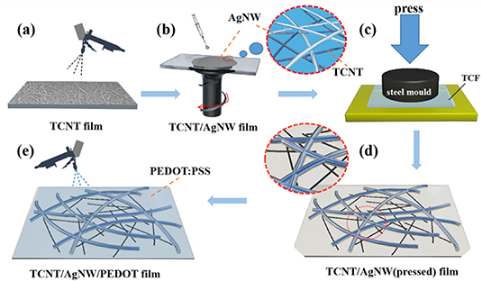
Figure 1. Schematic diagram of fabrication and post-treatment process of TCNT/AgNW-PET TCFs. (a) Spray-coating TCNT suspension on PET substrate; (b) spin-coating AgNW suspension on TCNT film and construct TCNT/AgNW double-layer conductive network structure. The post processing of TCNT/AgNW films by mechanical pressing (c) and (d), and covering PEDOT:PSS (e).
Download figure:
Standard image High-resolution image2.5. Fabrication of OLED
We used TCNT/AgNW/PEDOT-PET TCF as the anode, and then PEDOT:PSS were spin-coated on TCF at 2000 rpm to increasing the TCF work function. The films were then transferred into a high-vacuum chamber (operating pressure below 7  10−4 MPa) to deposit the following organic and metal materials. The OLED used 60 nm Alq3 as a light-emitting layer, 0.8 nm LiF as an electron injection layer, and 120 nm Al as the cathode. All of the organic materials were evaporated with the mask and using the quartz-crystal to monitor the deposition rate.
2.6. Characterization
The optical transmittance of the films was measured by ultraviolet-visible (UV–Vis) spectrophotometer at 550 nm while the sheet resistance of the films was measured using the four-point probe method (Keithley 2700 multi-meter). The haze meter (NDH 7000) was used to measure film's haze. The morphology of the films was analyzed via Field-emission scanning electron microscopy (FE-SEM) (Hitachi S-4800) and atomic force microscopy (AFM, BRUKER). The surface wettability was assessed by a contact-angle analysis device (DSA100, KRUSS). Adhesive tape (Scotch Magic Tape, 3 M, USA) was utilized to evaluate the adhesion of the films. The performance of the OLEDs was characterized by an optical detection system for OLED display panels developed by Suzhou Fstar Scientific Instrument Co., Ltd.
3. Results and discussion
Figure 2(a) shows the process of TA non-covalently modifying carbon nanotubes. Tannic acid molecules that widely exist in natural plants are anchored on the walls of carbon nanotubes by π-π interaction [35–37]. Due to the existence of a large number of phenolic hydroxyl groups in tannic acid molecules, the water contact angle of the CNT film decreased from 113° before modification to 54°. The non-covalent modification of TA not only improved the hydrophilicity of TCNT, but also demonstrated retains the excellent electrical conductivity of SWCNT (in figure 2(b)). Such a result mainly benefits from the modification process that occurs under mild non-covalent conditions did not damage the original electrical structure of SWCNT [38–40]. For other characterization of TCNT, please refer to our previous work [37].
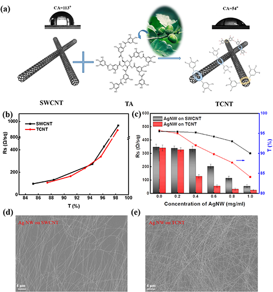
Figure 2. (a) Schematic depiction of TA modified SWCNTs. (b) The relationship between the transmittance (@550 nm) and sheet resistance of the TCNT and SWCNT films. (c) The change of transmittance and sheet resistance of different concentration AgNWs on SWCNT films, and TCNT films. SEM imagines of 0.8 mg ml−1 AgNWs spin-coated (2000 rpm) on (d) SWCNT and (e) TCNT films.
Download figure:
Standard image High-resolution imageTo further confirm the role of TCNT in facilitated the spin-deposition of AgNWs, we spin-coated different concentrations of AgNWs on SWCNT and TCNT films with a transmittance of 96% (about 30 nm in thickness), respectively, to compare the change of transmittance and sheet resistance of the hybrid films (as shown in figure 2(c)). Compared with SWCNT film, with the increase of AgNWs concentration, the sheet resistance of TCNT-based film shows a faster decline rate. When the concentration of AgNW suspension is 0.4 mg ml−1, the sheet resistance of TCNT/AgNW hybrid film decreases significantly, while that of SWCNT/AgNW hybrid film does not show such a trend. When the AgNW deposition concentration is 0.8 mg ml−1, the sheet resistance of the SWCNT/AgNW hybrid film and TCNT/AgNW hybrid film are 113 Ω sq−1 and 31 Ω sq−1, respectively, and the corresponding light transmittances are 93.0% and 87.7%. Figures 2(d) and (e) show the SEM images of 0.8 mg ml−1 AgNWs spin-coated on SWCNT and TCNT substrates at 2000 rpm, respectively. More hydrophilic TCNT can attach more AgNWs to the substrate to form a denser conductive network, which significantly improves the efficiency of AgNWs spin-deposition and effectively avoids the waste of raw materials. Therefore, the hydrophilic TCNT acts more like a transparent conductive adhesive, anchoring AgNWs with better conductivity on the TCNT network, and mixing with them to form a double-layer conductive percolation network structure.
The morphology of TCFs can be obtained by scanning electron microscopy. Figure 3(a) shows a pure and dense spider-like TCNT network and figure 3(b) shows the double-layer conductive network structure formed by a randomly distributed AgNW network deposited on the TCNT layer. In such a double-layer structure, the highly conductive and large diameters AgNWs serve as the main transport channels for the carriers. The carbon nanotubes help the AgNWs add more paths for electron transfer [23]. It compensates for the conductive defects caused by many insulation openings in the AgNW network, increases the electrode's robustness, and forms a film structure similar to a two-dimensional planar conductor. However, in the AgNW network, the raised junctions (shown in the red circles) will seriously deteriorate the film roughness. To solve this problem, we introduced the post-treatment process of mechanical pressing and covering PEDOT:PSS to optimize film performance. Figure 3(c) shows the surface morphology of TCNT/AgNW film after 25 MPa mechanical pressing, and it can be found the junctions between AgNWs are welded instead of simply lapping (shown in the blue circles). The mechanical press of 25 MPa makes the network structure smooth and stable, and without damaging the underlying TCNT network (shown in figure S1 (available online at https://stacks.iop.org/NANO/32/015708/mmedia)). Subsequently, we sprayed 1.5 ml, 3.0 ml, and 4.5 ml volumes of DMSO modified PEDOT:PSS solution on the surface of the film after mechanical pressing, and prepared TCNT/AgNW/P(1.5), TCNT/AgNW/P(3.0), and TCNT/AgNW/P(4.5) films, and their SEM morphologies are shown in figures 3(d)–(f), respectively. It can be found that PEDOT:PSS completely encapsulates the TCNT/AgNW network. With the increase of PEDOT:PSS spraying amount, the morphology of the bottom hybrid network becomes fuzzier, and the surface of the film becomes flatter.
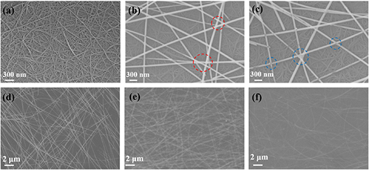
Figure 3. SEM images of (a) TCNT film, (b) TCNT/AgNW film, (c) TCNT/AgNW (pressed) film, (d) TCNT/AgNW/P(1.5) film, (e) TCNT/AgNW/P(3.0) film, and (f) TCNT/AgNW/P(4.5) film.
Download figure:
Standard image High-resolution imageAtomic force microscope was used to characterize and compare the changes in the surface topography and roughness of the hybrid film before and after post-treatment. Figure 4 shows the AFM images of pure AgNW film, TCNT/AgNW film, and TCNT/AgNW/P (3.0) film and their corresponding 3D AFM images. In figure 4(a), the raised junction of pure AgNW film makes the film root-mean-square (RMS) roughness reach 43.5 nm, and the RMS of TCNT/AgNW film is 41.0 nm. There is no significant difference between the two types of film roughness. The stacking of this double-layer network structure inevitably causes high roughness. The high roughness limits the application of TCF in optoelectronic devices, making it extremely prone to short circuits. After two-step post-treatment, the protruding junctions in the conductive network were flattened by mechanical pressing. Simultaneously, the smooth PEDOT:PSS layer could encapsulate the rough nano network, resulting in the RMS of TCNT/AgNW/P (3.0) film significantly reduced to 3.8 nm. With the further increase of the PEDOT:PSS spraying amount, the film roughness gradually decreased, and the RMS of TCNT/AgNW/P (4.5) film was only 1.2 nm.
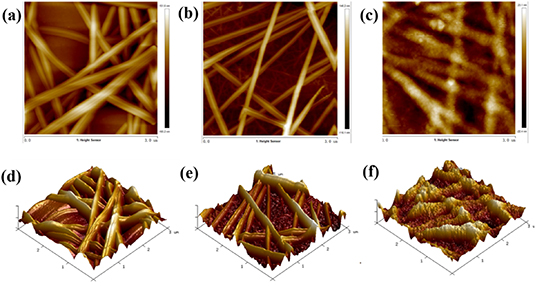
Figure 4. AFM topographic images and corresponding three-dimensional images of (a) and (d) pure AgNW film; (b) and (e) TCNT/AgNW film; and (c and f) TCNT/AgNW/P(3.0) film.
Download figure:
Standard image High-resolution imageTo further explore the effect of post-processing conditions of mechanical pressing and covering with PEDOT:PSS on the conductivity performance of the TCFs, we used TCNT/AgNW (0.8 mg ml−1) films (about 90 nm in thickness) with superior transmittance (87.7%) and sheet resistance (31.0 Ω sq−1) as the experimental samples, then press them under the mechanical pressure of 5 MPa, 10 MPa, 15 MPa, 20 MPa, and 25 MPa respectively for 10 min, and then 1.5 ml, 3.0 ml, and 4.5 ml of DMSO modified PEDOT:PSS solution was sprayed on each mechanically pressed films. The changes in their sheet resistance are shown in figure 5(a), where the dotted line shows the change of the sheet resistance of the film under the optimal post-treatment process of TCNT/AgNW film. At lower pressure (10 MPa), the sheet resistance of the film appears a significant decrease. After mechanical pressing at 25 MPa, the sheet resistance of the film decreased from 31.0 Ω sq−1 to 12.4 Ω sq−1, by 60.0%. Unlike mechanical pressing, we found that the post-treatment method of covering PEDOT:PSS cannot continuously reduce the sheet resistance of the hybrid film. Only spraying an appropriate amount of PEDOT:PSS solution can improve the conductivity of the hybrid film. For TCNT/AgNW films treated by mechanical pressing at 25 MPa, when the spraying amount of PEDOT:PSS was 3.0 ml (corresponds to ∼75 nm in thickness), the sheet resistance of the hybrid film showed the lowest value, decreased from 12.4 Ω sq−1 to 9.2 Ω sq−1, by 25.8%. While the sheet resistance increased to 24.3 Ω sq−1 after spraying 4.5 ml (corresponding thickness about 120 nm).
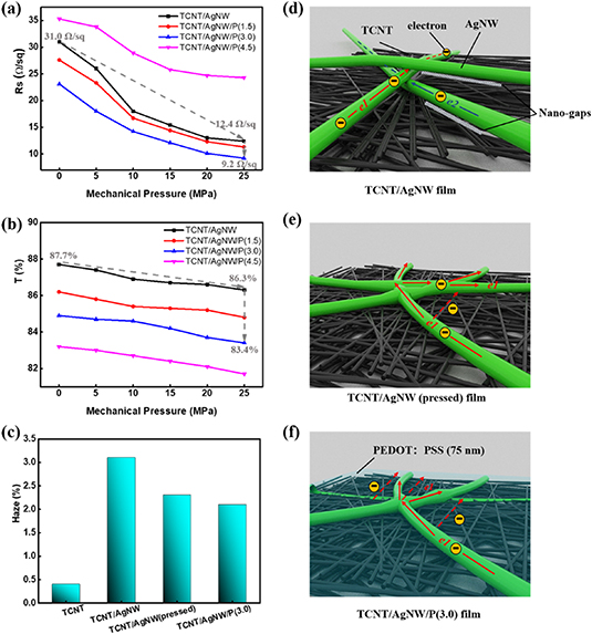
Figure 5. (a) Resistance and (b) transmittance change of TCNT/AgNW film after mechanical pressing and covering PEDOT two steps post-treatment. (c) The haze diagram of different types of TCFs. The schematic illustrations of conductive mechanism of (d) TCNT/AgNW film, (e) TCNT/AgNW (pressed) film, and (f) TCNT/AgNW/P(3.0) film.
Download figure:
Standard image High-resolution imageBased on the above experimental results, we have made reasonable assumptions about the conductive mechanism of the film during post-processing and shown in figures 5(d)–(f). Figure 5(d) shows the overlapping AgNWs with weak electrical contact deposited on the TCNT layer by spin coating before post-processing. Besides, the random overlapping structure makes the AgNWs and the TCNT layer have a large number of nano-gaps and only a few point contacts, which hinders the transfer of electrons from the AgNWs to the TCNT layer. These problems make the electrons need to overcome a large amount of energy during the transmission process at the NWs junctions and the contact points [18, 41]. Therefore, electrons are primarily transported in one direction in a single nanowire, and hardly through the junction and contact point in the double-layer conductive network [10] (simulated in figure 5(d) by e1 and e2), leading the films without post-treatment exhibit low conductivity. Figure 5(e) shows the conductive mechanism of the film after the mechanical pressing process. Same as figure 3(c), the junctions of the AgNWs are welded under the action of mechanical pressure, and the AgNWs form a stable surface contact with the TCNT layer. Such a stable connection can reduce the electrons transport barrier at the junctions of NWs and the contact points between NWs and nanotubes, so that the electrons can be transported in multi-directional in a single NW, NW-NWs, and NW-CNTs. This electrons transfer mechanism dramatically improves the conductivity of the hybrid films. After spraying 3.0 ml of PEDOT:PSS on the surface of the film, the electrical conductivity of the hybrid film is further increased, and the mechanism diagram is shown in figure 5(f). In the TCNT/AgNW/P(3.0) film, the PEDOT:PSS acts as a conductive binder for TCNT/AgNW network. The thin PEDOT:PSS layer (less than 75 nm) can fill the voids in the TCNT/AgNW film, repair the area of weak contact and broken circuit in the original structure [33, 42], and make the film form a three-dimensional conductor, so it can add more electronic transmission paths and effectively increase the conductivity of the hybrid film. However, the conductivity of the DMSO modified PEDOT:PSS is not as high as AgNW [25]; if the PEDOT:PSS layer is too thick, it will reduce the carrier transfer efficiency in the hybrid film, which undoubtedly makes the film exhibit low conductivity. Sulfuric acid or nitric acid post-treatment can improve the conductivity of PEDOT:PSS layer [43, 44], but it will destroy the AgNW network and cause environmental pollution.
Figure 5(b) shows the change of light transmittance of TCNT/AgNW film during post-treatment. Mechanical pressing causes a slight decrease in transmittance of the film and welding at the joint causes about 1.0% transmission loss. After that, the transmittance of the hybrid films decreased linearly with the increase of PEDOT:PSS spraying amount. The amount of 3.0 ml spray resulted in a decrease of 3.0% light transmission. Therefore, considering the roughness of the film and the conductivity performance of the film, we chose 25 MPa mechanical pressing and spraying 3.0 ml PEDOT:PSS as the best post-treatment conditions. Under the optimal post-treatment conditions, the sheet resistance of the TCNT/AgNW/P(3.0) film (about 110 nm in thickness) decreased from 31.0 Ω sq−1 to 9.2 Ω sq−1, decreased by 70.3%, and the transmittance decreased from 87.7% to 83.4%.
Figure 5(c) shows the change in the haze of different types of films. Compared with TCNT film, the haze of TCNT/AgNW has deteriorated significantly, rising from 0.4% to 3.1%. This defect is caused by the inherently high light-scattering characteristic of AgNWs [45]. High haze can cause blurriness if used as a transparent electrode of a display [46]. Excitingly, the post-treatment process of mechanically pressing and covering PEDOT: PSS can reduce the haze value of the film. After mechanical pressing, the haze of TCNT/AgNW(pressed) film decreased to 2.3%, decreased by 0.8%, while the haze value of TCNT/AgNW/P(3.0) film further decreased to 2.1%. As we all know, the internal haziness is related to the diameter of AgNWs, and external haziness is related to the coating uniformity and gaps between the AgNWs [47]. Mechanical pressing makes the AgNW network form a stable and uniform structure similar to a two-dimensional planar conductor, as well as the PEDOT: PSS layer fills the gap of the AgNW network, which effectively reduces the external haze of the film, thus effectively improving the haze of the film.
 and
and  represent the direct-current conductivity and optical conductivity of the films, respectively. In order to reveal the influence of different post-treatment conditions on the conductivity of TCFs, we introduce the value of
  to evaluate it. The relationship between the
  value and Rs and T in TCF satisfies the formula (1) [48].
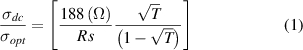
Figure 6 shows the  values of TCNT, TCNT/AgNW, TCNT/AgNW (pressed), and TCNT/AgNW/P (3.0), which are 24.0, 89.4, 198.3, and 215.1, respectively. The post-treatment of mechanical pressing and covering PEDOT:PSS significantly enhance the conductivity of the film. In table 1, we summarize the conductive performance and roughness of TCFs that have been similarly studied recently and compare them with our work. It can be found that maintaining the conductivity of AgNW-based films at low roughness is still a challenging task, and our work has better comprehensive performance compare to them.
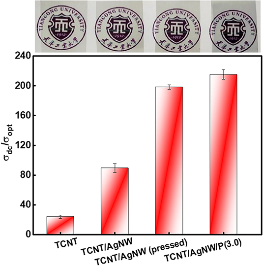
Figure 6.
 diagram of different types of TCFs (The insets correspond to the physical pictures of different types of films).
Download figure:
Standard image High-resolution imageTable 1. Comparison of performances with different types of transparent conductive films.
| Film | Rs (Ω sq–1) | T% |

| Roughness (RMS) | References |
|---|---|---|---|---|---|
| AuNPs-decorated AgNW film | 13.2 | 86.1 | 183.3 | – | [22] |
| AgNW-PEDOT:PSS film | 10.76 | 85 | 206.4 | 51.8 nm | [33] |
| AgNW/PDMS film | 9 | 82 | 200.2 | – | [8] |
| AgNW@iongel film | 8.4 | 86 | 285.7 | 30.5 nm | [41] |
| SWCNT/AgNW film | 30 | 95 | 241.2 | – | [7] |
| AgNW/PEDOT:PSS film | 19.3 | 84 | 106.9 | 19.6 nm | [25] |
| TCNT/AgNW/P(3.0) film | 9.2 | 83.4 | 215.1 | 3.8 nm | This work |
Besides excellent opto-electronic properties and low roughness, the TCNT/AgNW/P(3.0) films also showed excellent mechanical stability, adhesion, and durability. Figure 7(a) shows the sheet resistance change with the bending times at a bending radius of 5 mm. R is the sheet resistance of the film after the bending test, and R0 is the initial resistance of the film. After bending 10 000 times, the pure AgNW film showed apparent damage, and the sheet resistance increased by 1.9 times. Compared with pure AgNW films, TCNT/AgNW hybrid films improved the deterioration trend. After 10 000 times of bending, the sheet resistance of hybrid films only increased by 0.4 times. For TCNT/AgNW films, the total electrical properties are mainly determined by the contact resistance of the junctions between AgNWs. Therefore, the primary way to hold down the increase of the hybrid film resistance is to keep the stable connection of the junctions between the AgNWs [23]. The dense TCNT network with high flexibility and variability can withstand the high mechanical strain. Under 10 000 times of bending, the TCNT network below can buffer a large amount of strain from the substrate, reducing the impact and damage to the AgNW networks. After the mechanical pressure post-treatment, the junctions of AgNWs are welded, showing a smooth and stable conductive network until 8000 times of bending. By two steps post-treatment of the action of mechanical pressure and the strong capillary force of PEDOT:PSS solution [44], the sheet resistance of TCNT/AgNW/P (3.0) TCF does not change after 10 000 times of bending, showing ultra-high flexibility (shown the inset of Figure 7(a)).
Figure 7. (a) Resistance changes of different types of films as a function of the number of bending. The inset is the schematic diagram of TCNT/AgNW/P (3.0) film bending. (b) Transmittance changes of different types of films after tape testing. Photograph of the TCNT/AgNW/P(3.0) film as electrode at (c) flat and (d) bending state connected to a LED after the adhesion test.
Download figure:
Standard image High-resolution image3 M tape test was used to test the adhesion of different kinds of films. We prepared four types of TCFs with similar transmittance (about 87%) on the PET substrate by controlling the deposition amounts of nanomaterials in advance. We then tested their transmittance changes after the tape text (Figure 7(b)). The adhesion of pure AgNW film on PET substrate is weak, part of the AgNW coating is separated after the tape test, and the light transmittance rises to 95.0% after the test. The transmittance of TCNT/AgNW film increased to 92.4% after the test, 2.6% less than pure AgNW film, which proved that the TCNT layer promoted the adhesion of AgNW to the PET film. After the post-treatment of mechanical pressing and covering the PEDOT:PSS, the stable conductive network and the protective effect of the PEDOT:PSS layer further enhance the film adhesion, and the light transmittance after the tape test only increased by 4.3% and 1.3%, respectively. Figures 7(c) and (d) show the TCNT/AgNW/P(3.0) film application as a flexible electrode in connecting electronic devices. In the bending state, the film still shows high conductivity. This result indicates that the film has excellent potential application value in flexible and wearable devices.
To compare the films' chemical stability, we exposed different types of films to 85 °C and 85% relative humidity for 14 d to observe the change of film sheet resistance (in figure 8). The sheet resistance of pure AgNW film increased by 2.6 times after 14 d, while TCNT/AgNW films increased by 0.9 times. After two-step post-treatment, the sheet resistance of TCNT/AgNW/P(3.0) film only increased by 0.24 times within 14 d. Figures 8(b)–(d) show the micromorphology of different types of films after being placed in air for 14 d. By comparing figures 8(b) and (c) to figure 3(b) or (c), it can be found that the upper silver nanowires are oxidized to different degrees, which is the main reason for the increase in sheet resistance. However, for TCNT/AgNW hybrid film, TCNT conductive percolation network still plays a supporting role in electron transport because of its strong chemical resistance (as shown the inset of figure 8(c)), thus slowing down the increase process of sheet resistance. After being encapsulated by PEDOT:PSS, TCNT/AgNW network is isolated from air, thus avoiding direct exposure to air and being oxidized (figure 8(d)).
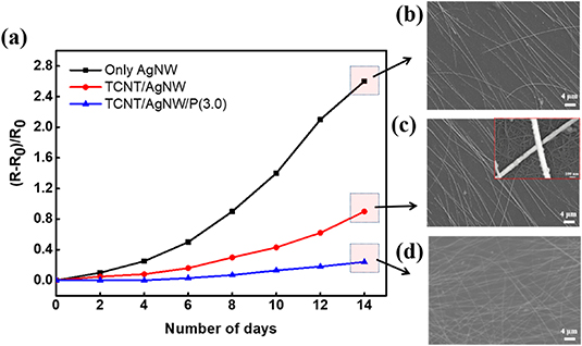
Figure 8. (a) Resistance changes of different types of films as a function of the number of days exposed to a high temperature and humidity chamber (Conditions: 85 °C temperature and 85% relative humidity). SEM images of (b) pure AgNW film, (c) TCNT/AgNW film (the inset is a high magnification imagine of (c)), and (d) TCNT/AgNW/P(3.0) film after exposure for 14 d.
Download figure:
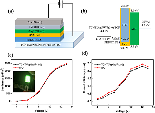
Standard image High-resolution imageTo verify the application ability of films in optoelectronic devices, we used TCNT/AgNW/P(3.0) films as anodes to prepare flexible OLED devices on PET substrates with a simple structure. For comparison, a device with the same structure based on commercial ITO-PET anode (Rs: 15 Ω sq−1, T: 90%) is used as a reference. The schematic structure of the device is shown in figure 9(a), and the energy level diagram of the device is illustrated in figure 9(b). Although TCNT/AgNW/P(3.0) has lower sheet resistance than ITO, its transparency is lower than that of ITO. Moreover, the work function of TCNT/AgNW/P(3.0) film is 4.4 eV, lower than that of ITO (4.8 eV), which weakens the ability of hole injection from anode to the organic layer, leading to the decrease of current density (as shown in figure 9(d)) [18]. Figures 9(c) and (d) shows the characterization of the performance of the OLED devices. The opening voltage of OLED devices with TCNT/AgNW/P(3.0) anode is 4.1 V, which is similar to that of the ITO electrode (3.9 V). Such low opening voltage proves that the ohmic contact between the two electrodes of the device and the active organic layer is well. At 13.0 V, the OLED device with TCNT/AgNW/P(3.0) anode showed a maximum luminance was 2428 cd m−2, while that of ITO anode is 2483 cd m−2. The maximum current efficiency was 2.31 cd A−1 at 12 V, while that of ITO anode is 2.45 cd A−1. Figure S2 shows the electroluminescence spectra of TCNT and ITO film devices, the peak value of the two devices keeps at about 515 nm without any shift. These results showed that the OLED with TCNT/AgNW/P(3.0) anode has comparable performance to the device with ITO anode. Figure S3 shows that TCNT/AgNW/P(3.0) films exposed to high temperature (85 °C) and humidity (85%) for 14 d still have similar performance when applied to OLED devices. This further confirmed the reliability of TCNT/AgNW/P(3.0) film and its great potential as a substitute for ITO film in flexible optoelectronic devices.
Figure 9. (a) The structure of green OLED devices. (b) The energy diagram of the OLED devices. (c) Voltage–luminance curve for the OLEDs. The inset shows a photograph of the OLED with TCNT/AgNW/P(3.0) anode in operation, being driven at 7 V. (d) Voltage–current efficiency curve for the OLEDs.
Download figure:
Standard image High-resolution image
4. Conclusion
We have developed a high-performance TCF with high conductivity, high transparency, low roughness, high adhesion, and excellent flexibility. Such outstanding performance is achieved by combining the construction of the TCNT/AgNW double-layer conductive network structure with the two-step post-processing technology of introducing mechanical pressing and covering PEDOT:PSS. TA modified CNTs greatly enhanced the deposition of AgNWs to the substrate. Mechanical pressing and PEDOT:PSS coating on the surface of the film as a post-processing step can effectively reduce the roughness and enhance the film's stability and reliability. In addition, the post-processing step has also been proved to improve the film's conductivity further. Finally, we successfully applied the transparent conductive film to OLED devices and obtained devices with excellent luminous intensity (2428 cd m−2) and current density (2.31 cd A−1). We believe that the experimental design ideas provided by us have certain reference values for the development of various stable and efficient, flexible transparent electronic devices.
Acknowledgments
The authors gratefully acknowledge financial support from the Natural Science Foundation of Tianjin China (Grant No. 19JCZDJC37800), the Natural Science Foundation of Jiangxi Province China (Grant No. 20181s206008), and the Science and Technology Plans of Jingdezhen China (Grant No. 20182GYZD011-06).