

Abstract
Measurements of minority carrier lifetime have been carried out on nonintentionally doped HgCdTe(100) layers grown by metal organic chemical vapor deposition on GaAs substrates. The studies have been carried out in order to investigate the possibility of applications of HgCdTe(100) epilayers to fully depleted P–i–N photodiodes operated at near-room temperatures and the background-radiation limit. Post-growth annealed layers show n-type conductivity with a residual donor concentration of about 1015 cm−3. The cadmium molar composition (0.262 < x < 0.336) was chosen for mid-wave infrared devices operating at 230 K to 300 K. Results show that at high temperatures, the samples show clearly Auger-limited lifetimes determined by the background doping. The measured lifetimes at 300 K range from 5 to 11 µs, and from 0.2 to 1 µs, for the cut-offs of 4 µm and 5.4 µm, respectively.
Export citation and abstract BibTeX RIS

Original content from this work may be used under the terms of the Creative Commons Attribution 4.0 license. Any further distribution of this work must maintain attribution to the author(s) and the title of the work, journal citation and DOI.
1. Introduction
Over the years, at the joint laboratory of Military University of Technology and VIGO System S.A. we have developed a semiconductor technology base for both n-type and p-type HgCdTe material relevant to high operating temperature (HOT) infrared (IR) detector design and fabrication [1, 2]. Complex HgCdTe heterostructure growth by metal organic chemical vapor deposition (MOCVD) on GaAs substrates has been used. Obtaining good quality HgCdTe layers on mismatched GaAs substrates has been quite a challenge, however, due to the potential reduction of production costs, as well as the ability to use optical immersion integrated with the detector [2, 3], it is a necessary choice. A unique feature of detectors with immersion lenses is the integration of photoelectric and optical functions, ensuring higher detectivity and speed of response.
Initially, HgCdTe layers with (111)B plane orientations have been used for photoconductors, photoelectromagnetic devices and photovoltaic devices. This was motivated by some advantages of the HgCdTe(111)B layers, most of all the lack of surface pyramid-shaped macro-defects known as 'hillocks', but also the large growth rate, low consumption of precursors and effective n-type doping with iodine up to 1018 cm−3. The growth in the (100) plane has been extensively used by British workers [4]. The HgCdTe(100) layers exhibit a better crystalline quality and significantly less residual donor concentration in the middle of 1014 cm−3 [5]. The high background concentration for (111) orientation is attributable to the presence of micro-twins [6]. The residual background concentration is a matter of a huge concern for engineers in semiconductor laboratories all over the world. For example, CEA-LETI shows the residual doping at the level of 1015 cm−3 for HgCdTe epilayers [7] while the range of low doping that is reproducibly generated in Teledyne is about 1013 cm−3 [8]. The technology of both groups is based on the molecular beam epitaxy. However, the most serious drawback of the HgCdTe(100) layers is the presence of hillocks with a density that is often above 103 cm−2 [9, 10]. The defect height is close to the thickness of the HgCdTe layer, which significantly hinders the further processing of detectors.
Recently, significant progress has been reported in our laboratory concerning the HgCdTe(100) materials, particularly associated with the reduction of surface defects below 102 cm−2 [11]. Hillocks tend to group on a substrate, which makes it possible to obtain a defect-free layer of a few square centimeters. The reproducibility of the production of optimized layers is sufficient for the processing of single pixel detectors, as well as small mosaics and lines of detectors.
The minority carrier lifetime is of particular importance in device design. We present some of our recent data for nonintentionally doped mid-wave IR (MWIR) HgCdTe(100) and compare them with currently accepted theories of generation–recombination (g–r) mechanisms.
2. Experimental
HgCdTe(100) layers were grown in a horizontal Aixtron AIX-200 MOCVD system. The growth was carried out on two-inch, epi-ready, semi-insulating (100) GaAs substrates, oriented 2°–6° off toward the nearest <110>. The growth process consists of few steps: (a) removal of oxides from GaAs substrates by annealling at 600 °C, (b) nucleation and growth of CdTe buffer layer, (c) growth of the detector heterostructure, and (d) controlled cooling to room temperature under mercury-rich conditions.
The growth was carried out at a temperature of about 350 °C and a mercury zone at 170 °C using the interdiffused multilayer process technique [12, 13] applied for the HgCdTe deposition at 0.5 bar. Electronic grade diisopropyltelluride and dimethylcadmium were used as Te and Cd precursors, respectively. Elemental mercury was used in a quartz bath as Hg precursor. H2 was used as the carrier gas.
Typically, 2–3 µm thick CdTe layer was used as a buffer layer, reducing stress caused by a crystal lattice misfit between GaAs substrate and HgCdTe structure. A cadmium flush during the nucleation process provides (100) CdTe growth [14]. The II/VI mole ratio was kept in the range from 1.5 to 5 during CdTe cycles. Selected growth parameters to obtain good quality HgCdTe(100) layers are listed in table 1. The growth of the hillock-free layers proved to be a critical process. The reduction of hillock density to <102 cm−2 has been achieved after modifications of several important aspects of the growth procedure, such as: substrate preparation, prenucleation treatment of the substrate in cadmium flux, selection of proper CdTe buffer and HgCdTe growth parameters, wafer rotation rate and even some modifications of the reactor design.
Table 1. Selected growth parameters of (100) HgCdTe layers.
| Prior to growth treatment | 600 °C/5 min | |||
| Nucleation condition | Cd flush | |||
| Growth pressure | 500 mbar | |||
| Susceptor temperature | 350 °C | |||
| Mercury zone temperature | 170 °C | |||
| II/VI ratio | 1.5–5 during CdTe cycles | |||
| Wafer rotation rate | 30–45 sccm | |||
| H2 gas flow rates | HgTe | Reactor gas artery | Upper | 100 sccm |
| Lower | 600 sccm | |||
| CdTe | Reactor gas artery | Upper | 1800 sccm | |
| Lower | 600 sccm | |||
The resulting layers show a high uniformity in both chemical composition and thickness, which is conditioned by the optimized precursors' fluxes, uniform heating and rotation of the substrate during the growth. The Cd composition was estimated by analyzing the FTIR transmission spectrum. The thickness of the HgCdTe layers was determined from the cleavage profile.
The carrier concentration was determined using 77 K fixed field van der Pauw-Hall measurements at a magnetic field of 0.5 T. The layers used for Hall effect measurements were processed into samples with four ohmic contacts.
The lifetime measurement was carried out using the photoconductive decay technique. The samples for the decay measurements were produced as photoconductors with a relatively thick uniform absorber layer sandwiched between graded gap structures (figure 1) to prevent the recombination at the surface and interface with the CdTe buffer. The devices were supplied with two ohmic contacts. The distance between contacts was sufficiently large (~1 mm) to prevent reduction of the signal decay time by the diffusion and hole drift sweep-out effects [15]. Laser diodes were used as a source of radiation pulses of subnanosecond rise and fall times. The light intensity was kept low in order to satisfy the low-injection condition. The photocurrent generated by the devices were read out with a fast transimpedance preamplifier that also provided a constant bias voltage applied to the devices. Finally, the amplified signal was analyzed with a fast digital oscilloscope.

Figure 1. Schematic cross section of HgCdTe heterostructure photodetector.
Download figure:
Standard image High-resolution imageFigure 2(a) shows an example of the relaxation curve for the HgCdTe(100) photoconductor with a 5.3 µm thick active layer and a molar composition of 0.325. The initial part of signal decay was often somewhat distorted by saturation of the device and other effects, so the response was fitted with an exponential function 3 µs from the end of the laser diode pulse. The time constant of the analyzed device is of about 8.52 µs, and with a specific design of the photoconductor can be considered as determined by the minority carrier lifetime. The spectral response of the same photoconductor is presented in figure 2(b). The cut-off wavelength, λc, of the device was determined at 10% of the signal value. The presented device has a cut-off wavelength of 4.25 µm at 300 K.

Figure 2. Time response (a) and spectral response (b) for the HgCdTe(100) photoconductor with a 5.3 µm thick active layer and a molar composition of 0.325. Detector operation temperature is 300 K.
Download figure:
Standard image High-resolution image3. Theory
The carrier lifetime in narrow-bandgap semiconductors is determined by the Auger, radiative and Shockley–Read–Hall (SRH) g–r processes. The Auger processes and radiative recombination are fundamental g–r mechanisms and are determined by the electronic band structure of the semiconductor. The SRH recombination is associated with defect states within the bandgap so it depends on the quality of the technology.
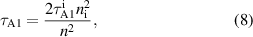
For n-type HgCdTe, the Auger 1 mechanism is believed to be the dominant at near-room temperatures. The process is the direct band-to-band recombination and involves a three-particle interaction: a conduction band electron with a heavy hole and the excitation of another electron in the conduction band. It can be expressed by [16]:
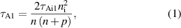
where n and p are the electron and hole concentrations, respectively, ni is the intrinsic carrier concentration, and τAi1 is the Auger 1 lifetime in intrinsic material:
Eg is the energy gap at a temperature T, kB is the Boltzmann constant,  is the static dielectric constant, q is the electron charge. µ must be taken as
  , where
  and
and  is the electron and hole effective mass, respectively. m0 is the free electron mass, F1
F2 is the overlap integral for Bloch functions. The last parameter consists of the largest uncertainty in the Auger model. Our theoretical estimations give the value of overlap integral F1
F2 between electron wavefunctions of 0.3.
is the electron and hole effective mass, respectively. m0 is the free electron mass, F1
F2 is the overlap integral for Bloch functions. The last parameter consists of the largest uncertainty in the Auger model. Our theoretical estimations give the value of overlap integral F1
F2 between electron wavefunctions of 0.3.
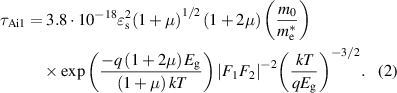
The standard theory of radiative recombination is given by van Roosbroeck and Schockley (VRS) expression [17]:
where
 is the high dielectric constant.
However, within the semiconductor, emitted photons can be re-absorbed and generate another electron–hole pair. This phenomenon is called the re-absorption effect or photon recycling (PR). It was shown by Humphreys [18] that the minority carrier lifetime is highly extended and depends on the semiconductor geometry and the strength of absorption coefficient. This was also shown in our numerical simulations [19], and this work shows that the VRS equation underestimates the carrier lifetime.
The SRH mechanism is not an intrinsic nor fundamental process because it occurs via trap levels associated with native defects or residual impurities, as well as with dislocations. In HgCdTe, the trap states located within the bandgap are associated with mercury vacancies [20, 21], so their elimination is highly desired. This has been achieved by the thermal anneal of the wafers at near-saturated Hg pressures during the programmed cooling down to room temperature.
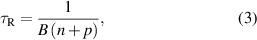
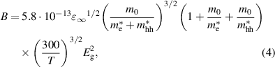
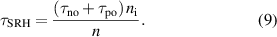
The carrier lifetime due to the SRH g–r process in n-type HgCdTe is associated with neutral centers located at the intrinsic energy level in the semiconductor bandgap [22]. Then, for the field-free region in an n-type material [23, 24]:
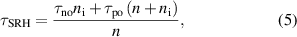
where τno = (γn Nr)−1, and τpo = (γp Nr)−1. The Nr is the density of SRH centres and γn and γp the respective recombination coefficients for electrons and holes. At low temperatures, when n > ni, we have τSRH ≈ τpo in the field-free region. At high temperatures, when n ≈ ni, we have τSRH ≈ τno + τpo.
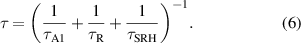
Under the condition of a small excess carrier concentration, the lifetimes associated with these processes can be treated as independent. The bulk carrier lifetime can then be written as:
4. Results
Undoped, post-annealed HgCdTe layers show n-type conductivity with a background donor concentration determined by residual dopants. Figure 3 presents the Hall concentration at 77 K versus Cd molar composition for a series of HgCdTe(100) samples. The background donor concentration obtained in our system ranges from 5 × 1014 cm−3 up to 2.5 × 1015 cm−3, regardless of molar composition. Our best results are comparable to the values reported by CEA-LETI [7]. The matter of a residual donor concentration is particularly important during p‐type doping at the low level, but what is most important is to determine the carrier lifetime.

Figure 3. Residual background concentrations of undoped HgCdTe(100) layers versus Cd molar composition.
Download figure:
Standard image High-resolution imageThe relative importance of the Auger 1 and radiative g–r processes in n-type HgCdTe is illustrated by calculating the lifetime for different cut-off wavelengths. The calculations were compared with the experimental data taken at 230 K and 300 K for several dozen HgCdTe(100) layers (figure 4). The Auger 1 and radiative lifetime were calculated using equations (1)–(4), respectively. In high-quality material, the SRH lifetime does not play an important role, especially at elevated temperatures conditions, and was not considered in the calculations. So the total bulk carrier lifetime was calculated using equation (6) assuming only the Auger 1 and radiative contributions. In our calculations of the carrier lifetime, we have assumed an electron concentration of 1.3 × 1015 cm−3, corresponding to the average value obtained by the Hall effect measurements on the whole samples (see dashed line on figure 3). The expressions for Eg and ni were the ones from Hansen and Schmit [25]. The dielectric constants are not a linear function of composition, while the temperature dependence was not observed within the experimental resolution [26]. All other fitting parameters have been summarized in table 2.

Figure 4. Calculated and experimental minority carrier lifetime as a function of cut-off wavelength for n-type HgCdTe at 230 K (a) and 300 K (b). The calculated lifetimes were assumed to be determined by Auger 1 and radiative recombination mechanisms.
Download figure:
Standard image High-resolution imageTable 2. Selected parameters taken in calculations of Auger 1 and radiative lifetimes in n-type Hg1-x Cdx Te.
| Bandgap energy, Eg (eV) |

|
| Intrinsic concentration, ni (cm−3) |

|
| |
Electron effective mass, 
| 0.071Eg |
Hole effective mass, 
| 0.65 |
| Overlap integral, F1 F2 | 0.3 |
Static dielectric constant, 
|

|
High-frequency dielectric constant, 
|

|
| Electron concentration, n (cm−3) | 1.3 × 10¹⁵ |
According to the traditional VRS theory, the radiative recombination should determine the carrier lifetime, especially at room temperature and in the short-wave IR. As shown in figure 4, the experimental results exceed the total lifetime of the carriers at room temperature over the entire analyzed wavelength range, and at 230 K for wavelengths below 4.5 µm, and the total value of the carrier lifetime is significantly underestimated. As a results of the reabsorption of photons generated within the semiconductor by the radiative recombination, the radiative carrier lifetime increases by orders of magnitude. Then, the minority carrier lifetime is limited by the Auger recombination. When the Auger mechanism is dominant, the omission the PR effect in the calculation of a radiative carrier lifetime it is so noticeable (at 230 K and for wavelengths above 5 µm). Summing up, it can be stated that the PR effect occurs in the tested samples, and the minority carrier lifetime is limited by the Auger 1 mechanism—a good fit of Auger 1 lifetime to the experimental results have been successful achieved for both analyzed temperatures over the entire wavelength range.
Figure 5 shows the calculated and measured lifetime as a function of the Hall carrier concentration determined at 77 K for n-type MWIR HgCdTe at temperatures of 230 K and 300 K. The experimental data were collected for samples with a similar Cd molar composition and the calculations were made for x = 0.268. Here we can also see that using classical VRS theory to calculate the radiative carrier lifetime, the resultant total lifetime is underestimated. The experimental results agree well with the Auger 1 theory.

Figure 5. Calculated and experimental minority carrier lifetime as a function of Hall carrier concentration determined at 77 K for n-type HgCdTe at 230 K (a) and 300 K (b). The calculated lifetimes were assumed to be determined by Auger 1 and radiative recombination mechanisms.
Download figure:
Standard image High-resolution imageAccording to equation (1), at low temperatures, where nH77K > ni (nH77K is the Hall concentration at 77), the Auger 1 lifetime decreases with the square of the carrier concentration. At high temperatures, where ni > nH77K, the Auger 1 lifetime becomes independent of the electron Hall concentration at 77 K, which is especially confirmed by the measurement at 300 K (figure 5(b)). The experimental carrier lifetime is independent of the 77 K Hall electron concentration determined by residual dopants up to the value of 2 × 1015 cm−3.
5. HOT HgCdTe photodiode
The obtained results may be used to optimize the material parameters required for the high-temperature operation of HgCdTe photodiodes. It can be assumed that the thermal annealing during the controlled cooling used in our technology effectively reduces the concentration of metal vacancies, which determine the SRH lifetime. As referred to earlier, due to the presence of the PR effect, it is also possible to eliminate the internal radiative g–r process. Under these circumstances, it will be beneficial to operate the HOT device with a highly reduced concentration of minority and majority carriers in the active volume, as in the case of the P–i–N diode operating in nonequilibrium conditions [27, 28].
The successful operation of the P–i–N photodiode requires the use of non-injection contacts. In this case, it is fulfilled by the heterojunction to the P+ and N+ volumes ('+' stands for the heavily doped area and a capital letter stands for a wider bandgap). Under a moderate reverse bias (see figure 6(a)), the minority carriers (holes) thermally generated at the absorber are fully extracted, while the majority carrier (electron) concentration is reduced to the doping level that causes a suppression of the Auger g–r process.

Figure 6. Energy band diagram of P–i–N photodiode operated under nonequilibrium conditions (a) and with fully depleted absorber (b).
Download figure:
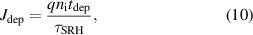
Standard image High-resolution imageThe dark current of the Auger-suppressed P–i–N photodiode operated under nonequilibrium conditions is the sum of the diffusion and depletion currents. The diffusion current arises from the thermal generation of carriers in a thick, undepleted absorber. The diffusion current density derived from the Auger and SRH generation in n-type semiconductor is:
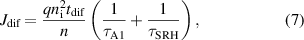
where tdif is the diffusion region thickness.
At nonequilibrium conditions, when the majority carrier concentration is held equal to the majority carrier doping level (and intrinsically generated majority carriers are excluded (p ≪ n ≈ Nd)), equation (1) becomes:
and equation (5) becomes:
The depletion current arises from the portion of the absorber that becomes depleted and can be estimated as:
where tdep is the width of depletion region, expressed as
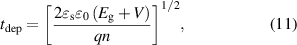
 is the vacuum permittivity,
  is the applied bias. For the depletion region, the effective SRH lifetime is τSRH ≈ τno+ τpo.
A comparison of the temperature dependence of the Auger 1 and SRH lifetimes in the equilibrium and nonequilibrium modes is shown in figure 7 for n-type MWIR HgCdTe with Cd molar composition of x =0.268 and doping concentration of 1.3 × 1015 cm−3. Calculations have been carried out with the assumed value of the SRH carrier lifetime of τno= τpo = 50 µs. Lower SRH values would reduce the total time, which would not be in compliance with the measured values shown in figure 5. The equilibrium SRH recombination in the n-HgCdTe exhibits a mild temperature dependence over the extrinsic to intrinsic temperature range, varying by a factor of 2. Under the non-equilibrium mode, the SRH lifetime exhibits a temperature dependence given by ni. The strong increase of the SRH lifetime at high temperatures is caused by the decreasing of electron population, what in consequence results in the decreasing of the minority carriers capture rates [22]. Also in the case of the Auger 1 mechanism, the difference between the equilibrium and non-equilibrium mode is significant at high temperatures. Thus, there is no fundamental limitation for HgCdTe IR detectors to achieve the background limited performance (BLIP) at a room temperature [29].

Figure 7. Calculated equilibrium and nonequilibrium Auger 1 and SRH minority carrier lifetime versus inverse temperature for n-type MWIR HgCdTe with Cd molar composition of x = 0.268 and doping concentration of 1.3 × 1015 cm−3. Calculations have been done with the assumed value of SRH carrier lifetime of τno= τpo = 50 µs.
Download figure:
Standard image High-resolution imageKinch, in his monographs [22, 30], and recently, Teledyne [8], have proposed the P–i–N HgCdTe photodiode with a fully depleted absorber as the future of HOT IR devices. Under a relatively strong reverse bias (see figure 6(b)), free carriers (both electrons and holes) are immediately separated by the local electric in the fully depleted absorber and the Auger g–r process is completely eliminated. Thus, the dark current of the fully depleted P–i–N photodiode is limited only by the depletion current given by the equation (10) with the carrier concentration reduced to zero.
We also compare the temperature relation between the diffusion and depletion currents for the Auger-suppressed P–i–N HgCdTe photodiode and the same photodiode but operating with a fully depleted absorber (figure 8). Calculations have been done for a Cd molar composition of x = 0.268, doping concentration of 1.3 × 1015 cm−3 and the thickness of the active region of t = 5 µm. Calculations are also compared with the semiempirical rule, 'Rule 07' (specified in 2007) for P-on-n HgCdTe photodiodes [31], and the background radiation current. At a low bias regime, the depleted region occupies the active region to the depth of ~1 μm. The dark current is determined by the diffusion component at temperatures above 120 K, and by the depletion component at low temperatures. In this case, the diffusion current is comparable to those specified by the 'Rule 07'.

Figure 8. Diffusion and depletion current components versus temperature for MWIR HgCdTe P–i–N photodiode with Cd molar composition of x = 0.268, doping concentration of 1.3 × 1015 cm−3 and the thickness of the active region of t = 5 µm. Calculations have been done with the assumed value of SRH carrier lifetime of τno= τpo = 50 µs.
Download figure:
Standard image High-resolution imageWhen the absorber is fully depleted, the dark current at 300 K is over an order of magnitude smaller than that described by the 'Rule 07'. However, by assuming the value of the SRH carrier lifetime of τno= τpo = 50 µs, it is still several times higher than the background radiation current. In this case, it is necessary to obtain the highest possible carrier lifetimes associated with the SRH mechanism. In the MWIR range, the lowest τSRH value is ~150 µs [30] so that the depletion current is equal to the background radiation current (figure 9). What is more, for the absorber doping level of 1.3 × 1015 cm−3, a 5 μm thick absorber can be fully depleted at the sufficiently high reverse bias (~17 V, see figure 10), at which the tunnel component will dominate currents in the real device. Further technological progress is required to reduce the residual carrier concentrations below 1014 cm−3 for the bias voltage that fully deplete a 5 μm thick absorber without the tunneling. Moreover, the absorber thickness and the bias voltage necessary to make it completely depleted can be significantly reduced without the loss of quantum efficiency by using enhanced absorption methods, e.g. reflections from the back surface (double enhancement), and far more strongly for an optical cavity or plasmonics.

Figure 9. Calculated SRH lifetime versus temperature for which the depletion dark current of fully depleted P–i–N HgCdTe photodiode is equal to the background radiation current.
Download figure:
Standard image High-resolution image
Figure 10. Calculated reverse bias voltage versus doping concentration required to deplete a 5 µm thick MWIR HgCdTe absorber.
Download figure:
Standard image High-resolution image
6. Summary
The limiting lifetime mechanisms in n-type HgCdTe(100) layers grown by MOCVD on GaAs have been discussed. Experimental values exceeding the theoretical estimates assuming the VRS expression for the radiative recombination prove the occurrence of the PR effect significantly extending the radiative lifetime. At temperatures achievable within the thermoelectric coolers, the SRH mechanism also does not affect the carrier lifetime in the diffusion volume of the semiconductor. MWIR HgCdTe(100) layers show clearly the Auger-limited recombination and the only limitation in this case is a relatively large residual background doping. Under these circumstances, it will be beneficial to operate the HOT device with no majority carriers in the active volume, as in the case of the P–i–N photodiode operating in nonequilibrium conditions. Then, for a fully depleted absorber, the Auger g–r process can be completely eliminated, and the dark current of the photodiode will be limited only by the SRH mechanism derived from the depleted absorber. In order to take advantage of operations with a depleted absorber, the lowest possible background doping, much below 1014 cm−3, should be obtained in order to reduce the reverse bias voltage necessary to completely deplete the absorber, as well as the highest possible SRH carrier lifetimes being obtained to reach BLIP conditions at room temperature.
Acknowledgments
This work has been supported by the National Science Centre (Poland), Grant No. 2017/27/B/ST7/01507.