

Abstract
A 60 GHz third-order on-chip bandpass filter (BPF) based on half-mode substrate integrated waveguide (HMSIW) cavity is synthesized using GaAs pHEMT technology. Two coupling slots are etched to divide the HMSIW cavity into three resonators, and then a third-order Chebyshev BPF is designed with predicted transmission zero, return loss and bandwidth through the synthesis method. The theoretical and extracted external quality factor and coupling coefficients are used to determine the dimensions of the BPF. For demonstration, a BPF sample with a bandwidth of 29.2% is fabricated, and its simulations and measurements are in good agreement.
Export citation and abstract BibTeX RIS
1. Introduction
With the fast development of the fifth-generation (5G) and next-generation communications, designing millimeter-wave high-integration on-chip bandpass filters (BPFs) has been of great interest recently. Several semiconductor technologies are applied for the design of the BPFs, such as flexible polyimide substrate [1], compound column III–V [2–8], and SiGe/CMOS [9–16]. Especially, the design of 60 GHz on-chip BPFs has been a hot research topic since this frequency band is a promising solution to future Gb/s wireless communication.
In [8], an E-shaped dual-mode resonator and a stepped impedance resonator are used to construct a two-pole BPF at 60 GHz, whose design method is inspired from the filter topology fabricated on the printed circuit boards. In [9], a square ring one-wavelength resonator with a perturbation patch is employed to design a 60 GHz dual-mode BPF, and this method is often adopted for the filter design at low frequency, where the characteristics and size of the BPF are hardly improved. In [10] and [12], two second-order BPFs working at 60 GHz are presented using CMOS technology, but it is difficult to extend the design of higher order BPFs with low loss.
The GaAs pHEMT-based technology has been widely applied in communication circuits and systems. So far, few work on the synthesis of the millimeter-wave on-chip BPFs using GaAs technology has been presented. In this paper, using a half-mode substrate integrated waveguide (HMSIW) cavity, a third-order GaAs-based BPF working at 60 GHz is synthesized and fabricated. The measured results show that the proposed BPF has wide bandwidth and high frequency selectivity, which are in good agreement with the simulated ones. It validates the correctness of the synthesis method for the on-chip BPF.
2. Synthesis of 60 GHz third-order on-chip BPF
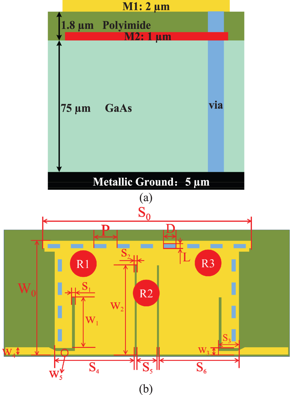
Figure 1 shows the proposed on-chip BPF based on HMSIW cavity using 0.15 µm GaAs pHEMT technology, where the relative permittivities of the GaAs and polyimide films are 12.9 and 2.9, respectively. The symmetrical structure of this filter consists of two microstrip feed lines and one HMSIW cavity with four slots etched on the top metal layer (i.e. M1 layer). The M2 layer as seen in figure 1(a) is not used in this work. Two slots in the middle as the coupling slots can be seen as capacitors, which provide the electric coupling between the adjacent resonators. Therefore, the HMSIW cavity is divided into three resonators, namely, Resonator 1 (R1), Resonator 2 (R2) and Resonator 3 (R3). It should be noted that R1 and R3 are quarter-mode SIW resonators, whereas R2 is a quarter-wavelength microstrip resonator. Besides, another two slots near the feeding as matching slots are used to achieve the desired impedance matching between the feed lines and the HMSIW cavity. As shown in the layout of the proposed filter, the transversal length of R2 (S5) is shorter than R1 and R3, which is different from the BPF with same dimensions of resonators in [17]. Therefore, the cross coupling between nonadjacent resonators should be taken into consideration, which will introduce a transmission zero (TZ) to the response of this proposed BPF.

Figure 1. (a) Stack-up of the employed 0.15 µm GaAs pHEMT technology. (b) Layout of the proposed BPF.
Download figure:
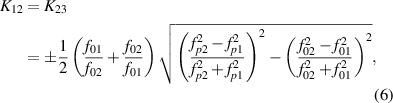
Standard image High-resolution imageThe coupling scheme of the proposed structure is shown in figure 2, where Qe is the external quality factor and Kij (i, j= 1, 2, 3, i≠ j) is the coupling coefficient. The K12 and K23 represent the coupling coefficients between two adjacent resonators while K13 is the coupling coefficient between two non-adjacent resonators R1 and R3. According to the coupling mechanism, the frequency response of the BPF can be determined by the values of the external quality factor and the coupling coefficients.
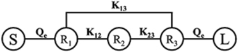
Figure 2. Coupling scheme of the proposed structure, where S and L represent source and load ports, respectively.
Download figure:
Standard image High-resolution imageGenerally, the values of Qe and Kij can be derived through the synthesis method of filters [18]. If the third-order Chebyshev filter (N = 3) is designed to have the predicted TZ at the angular frequency of +1.7 and return loss of 15 dB in passband, the (N + 2) coupling matrix M1 can be synthesized and expressed as follow:
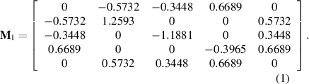
It is obvious that the matrix (1) has the transversal coupling structure, which is not suitable for the proposed BPF. However, M1 can be transformed to the folded form by similarity transforms [18]. Consequently, the coupling matrix of the folded network is transferred as:
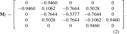
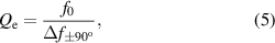
The Qe and Kij can be calculated from the entries of M2 by [19]:
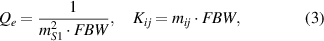
where FBW is the fractional bandwidth of BPF. Here, the center frequency of 60 GHz and the FBW of 30% are as the design specifications of BPF. Accordingly, the theoretical Qe and Kij are calculated as:


The calculation results of coupling coefficients in (4b ) and (4c ) are the absolute values, because only the magnitudes of coupling coefficients are needed to determine the physical dimensions of the coupling slots [18].
To obtain the proper dimensions, the actual values of external quality factor and coupling coefficients are extracted using the full-wave electromagnetic simulation software Ansys HFSS. Firstly, the dimensions of the HMSIW cavity is adjusted to get its resonance frequency of 60 GHz. Then, according to the coupling mechanism, the cross coupling between R1 and R3 (i.e. K13) is of great importance on the generation of TZ. The location of the TZ will be changed against the value of K13. However, it is difficult to accurately extract K13 through simulation to fit well with the theoretical value of K13. This is due to the fact that the resonator R2 is placed along the coupling path of R1 and R3, resulting in K13 dependent on the dimensions of the resonator R2 mainly. Therefore, we should simulate different values of S5 to meet the theoretical value of K13. And the dimensions of R1 and R3 can be calculated based the size of HMSIW cavity and R2. After that, the external quality factor and coupling coefficients could be extracted easily.
According to the theory of coupled resonators, the external quality factor can be numerically extracted by simulating an individually loaded resonator based on driven-mode through the following equation [19]:
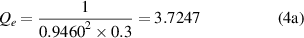
where f0 denotes the resonance frequency at the excitation port of the first resonator (i.e. R1 or R3) in the HMSIW cavity, and Δf±90°is determined from the frequency at which the phase ±90° with respect to the absolute phase at f0. Figure 3 depicts that the extracted Qe is dependent on the slot width S1 and the slot length W1. As W1 increases, the external quality factors for different values of S1 will all decrease. For the same slot length W1, the Qe will be gradually reduced as S1 increases.

Figure 3. Extracted external quality factor Qe versus S1 and W1.
Download figure:
Standard image High-resolution imageFurthermore, the coupling coefficients can also be extracted through the eigenmode simulation of the two coupled resonators using the following formula [19]:
where f01 and f02 denote the self-resonant frequencies of R1 and R2, respectively, fp1 and fp2 represent the two resonance frequencies of the coupled resonators. All the resonance frequencies can be obtained through eigenmode simulations. The extracted results of coupling coefficients versus S2 and W2 are plotted in figure 4. It can be found that the larger the dimensions of the coupling slots are, the weaker the coupling between R1 and R2 will be.
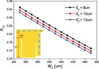
Figure 4. Extracted coupling coefficient K12 versus S2 and W2.
Download figure:
Standard image High-resolution imageBased on the theoretical values of Qe, K12 and K23 calculated in (4), the initial dimensions of the BPF are selected according to these extracted curves in figures 3 and 4. Then, the designed BPF is fine-tuned through the full-wave electromagnetic (EM) simulation software Ansys HFSS to compensate the influence from parasitic parameters. The final dimensions are tabulated in table 1.
Table 1. Dimensions of the proposed BPF.
| Parameter | Value (μm) | Parameter | Value (μm) | Parameter | Value (μm) |
|---|---|---|---|---|---|
| W0 | 561 | S0 | 1035 | S6 | 396 |
| W1 | 286 | S1 | 14 | P | 115 |
| W2 | 450 | S2 | 10 | D | 60 |
| W3 | 32 | S3 | 100 | L | 20 |
| W4 | 35 | S4 | 396 | ||
| W5 | 18 | S5 | 100 |
The synthesized frequency response derived from (2) and full-wave EM simulated response are both plotted in figure 5. The transmission poles and TZ of simulated results almost appeared in the same positions with those of synthesized results. Regardless of the loss influence, the simulated and synthesized S-parameters agree reasonably with each other, which verifies the correction of the synthesis process and the extraction of parameters.
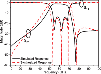
Figure 5. Comparison of the synthesized response and the simulated response.
Download figure:
Standard image High-resolution imageAccording coupled resonator theory, we can change the cross coupling and the main coupling to control the position of TZ. The cross coupling between R1 and R3 is mainly related with the dimensions of the resonator R2. However, the change of R2 will not only control the cross coupling, but also influence the main coupling between adjacent resonators. Therefore, we can choose the coupling slot as the key parameter to adjust the position of TZ, which is shown in figure 6. With the increase of W2 and S2, the coupling coefficient is decreased and the position of TZ shifts to lower frequency.
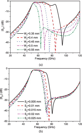
Figure 6. The position of TZ with different dimensions of coupling slots. (a) S2 = 0.1 mm, (b) W2 = 0.45 mm.
Download figure:
Standard image High-resolution image3. Implementation and measurements
For further demonstration of the proposed HMSIW BPF, the above mentioned example is fabricated and then measured via an on-wafer ground-signal-ground probing using a vector network analyzer. The measurement setup and die photograph of the proposed BPF are shown in figure 7.
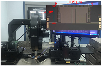
Figure 7. Measurement setup and die photograph of the proposed BPF.
Download figure:
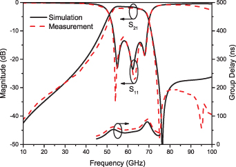
Standard image High-resolution imageThe simulated and measured S11 and S21 of the BPF are shown in figure 8, which agree well with each other. The measured results show that the presented BPF has a center frequency at 60.2 GHz with a 3 dB bandwidth from 51.4 to 69 GHz (i.e. 29.2%). The measured insertion losses are at the range between 1.99 and 2.72 dB within the passband, and the return losses are better than 13.9 dB. These results are basically coincident with the design specifications of BPF mentioned in section 2. The die photograph of the filter can be seen in the inset of figure 7. The chip size, excluding the feedings, is 1.035 mm × 0.561 mm. The performance comparisons between the proposed BPF and some reported works are tabulated in table 2.
Figure 8. Simulated and measured S-parameters and group delays of the proposed BPF.
Download figure:
Standard image High-resolution image
Table 2. Performance comparisons with some reported BPFs.
| Reference | f0 (GHz) | 3 dB FBW (%) | Insertion loss | Order of BPF | Circuit size (mm × mm) | Technology |
|---|---|---|---|---|---|---|
| [5] | 93 | 3.4 | 4.3 | 3 | 4.2 × 2.2 | ICP GaAs |
| [8] | 60 | 24.7 | 1.2 | 2 | 0.58 × 0.4 | IPD GaAs |
| [9] | 64 | 18.8 | 4.9 | 2 | 0.71 × 0.71 | 0.18 μm CMOS |
| [12] | 26.5 | 50.9 | 3.8 | 1 | 0.39 × 0.45 | 0.13 μm SiGe |
| [14] | 18 | 66.7 | 2.9 | 2 | 0.318 × 0.392 | 0.13 μm SiGe |
| This work | 60 | 29.2 | 1.99 | 3 | 1.035 × 0.561 | 0.15 μm GaAs |
The reference in the table means the reference, and FBW is the fractional bandwidth.
4. Conclusion
A 60 GHz on-chip BPF based on HMSIW cavity is proposed with a TZ at the upper stopband. Through the synthesis method, the theoretical values of external quality factor and coupling coefficients are calculated from a third-order Chebyshev BPF prototype, and then the dimensions of BPF are determined. The presented 60 GHz BPF has a broad bandwidth, low insertion loss and sharp roll-off skirt at the right edge of the passband, which can be readily applied in modern or even next-generation communication systems.
Acknowledgments
National Key Research and Development Program of China (2019YFB1803205); NSAF Joint Fund (U2130102); Natural Science Foundation of Shaanxi Province (2021JQ-060); State Key Laboratory of Advanced Optical Communication Systems Networks (2022GZKF020); Fundamental Research Funds for the Central Universities (xzd012020058); 'Siyuan Scholar' Fellowship of XJTU.
Data availability statement
The data that support the findings of this study are available upon reasonable request from the authors.