


Abstract
We experimentally demonstrate a three-dimensional plasmonic terahertz waveguide by lithographically patterning an array of sub-wavelength pillars on a silicon substrate. Doped silicon can exhibit conductive properties at terahertz frequencies, making it a convenient substitute for conventional metals in plasmonic devices. However, the surface wave solution at a doped silicon surface is usually poorly confined and lossy. Here we demonstrate that by patterning the silicon surface with an array of sub-wavelength pillars, the resulting structure can support a terahertz surface mode that is tightly confined in both transverse directions. Further, we observe that the resonant behavior associated with the surface modes depends on the dimensions of the pillars, and can be tailored through control of the structural parameters. We experimentally fabricated devices with different geometries, and characterized the performance using terahertz time-domain spectroscopy. The resulting waveguide characteristics are confirmed using finite element numerical simulations, and we further show that a simple one-dimensional analytical theory adequately predicts the observed dispersion relation.
Export citation and abstract BibTeX RIS

Content from this work may be used under the terms of the Creative Commons Attribution 3.0 licence. Any further distribution of this work must maintain attribution to the author(s) and the title of the work, journal citation and DOI.
1. Introduction
The use of sub-wavelength artificial structures to control and guide electromagnetic radiation is an area of growing interest and importance, especially in the terahertz spectral regime [1–6]. Artificially designed structures have led to new guided-wave devices with properties that can be engineered through the control of the structural parameters [7, 8]. Guided wave devices have been of significant interest for the scientific community for applications in sub-wavelength imaging [9], communication [10], slow light systems [11] and bio-sensing [12, 13]. Several waveguide geometries have been demonstrated at terahertz frequencies, including metal wires [14], parallel plate transmission lines [15], hollow polycarbonate waveguides [16] and corrugated metallic surfaces [17].
At terahertz frequencies, most metals behave as a perfect electrical conductor, which does not support a bound plasmonic mode at a planar interface. However, if the metallic surface is patterned or corrugated, the effective dielectric properties of the resulting effective medium can be altered such that the dispersion properties mimic those of surface plasmson-polaritons (SPPs). Pendry et al [7] first examined the propagation properties of the SPPs on a textured metal surface, and thereafter significant work has been reported on terahertz electromagnetic radiation propagation on corrugated metal surfaces. Highly confined guided mode propagation has been achieved, depending how the metal surface is designed [18–23].
The corrugations are believed to help in greater penetration of the field into the patterned structures in an effective medium model, thereby significantly reducing the exponentially decaying nature of the surface electromagnetic modes [24–27]. While patterning of a metallic surface can increase the binding of the surface waves and can be effective for guided wave devices, the fabrication of such structures is a non-trivial issue, especially at terahertz wavelengths where the required feature size is incompatible with conventional thin-film deposition and lithography methods. An alternative approach exhibiting the same propagation behavior at terahertz is required. Heavily doped silicon (n > 2.2 × 1019 cm−3) has been shown to exhibit metallic properties at terahertz frequencies [28, 29] and has the potential to replace metals in such applications. For the heavily doped silicon considered here, the Drude model predicts a relative permittivity of  = (− 1.3 + 2.0i) × 104 at 1 THz, which is large enough to be accurately modeled as a perfect electrical conductor. For comparison, the relative permittivity of gold at this frequency is calculated to be = (− 1.1 + 7.2i) × 105. An unpatterned silicon surface is capable of supporting surface electromagnetic waves that are highly delocalized in the lateral and transverse direction. We report here that by structuring the silicon surface using conventional deep reactive ion etching, one can achieve resonant guided-mode behavior as in metals. A periodic sequence of silicon pillars can have bound resonant modes that are highly confined to the surface both in transverse and lateral direction.
In this paper, we experimentally and numerically examine terahertz wave propagation on a heavily boron-doped silicon surface structured with pillars. We design and fabricate numerous waveguide patterns with varying heights of the pillars and characterize the wave propagation using THz time domain spectroscopy, a powerful tool for quantifying the magnitude and phase response. The structured silicon surface acts as an effective medium which can lead to highly confined terahertz guided mode propagation. The resonant modes supported by the waveguide structures are observed to be dependent on the dimensions of the pillars. Numerical simulations validate the experimental observations, and a one-dimensional (1D) theoretical model is found to be consistent with the observations.
In section 2, we discuss the dispersion relations of the fundamental resonant modes supported by the pillar waveguides with different heights of the pillars. In section 3, we describe the fabrication of the waveguides and experimental setup used for the characterization at terahertz frequencies. Section 4 presents the experimental terahertz measurements and corresponding simulation results for wave propagation on periodically patterned silicon substrates. In this section, we also describe how the geometrical properties of the structure relate to the resonant behavior of the fundamental mode, and compare the results with a simple analytical model originally developed for two-dimensional corrugations.
2. Dispersion properties of surface modes
Figure 1(a) depicts the schematic representation of the waveguide structure considered here with the relevant dimensions defined. The typical parameters for the waveguides considered here were w = 200 μm, l = 200 μm, p = 400 μm and heights from 100 to 400 μm.
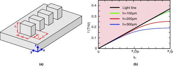
Figure 1. Schematic representation of the pillars structured on a highly doped silicon surface, with relevant dimensions and coordinate axes defined. (b) Numerically calculated dispersion properties of the fundamental terahertz surface mode. The solid black line corresponds to the light line for plane wave propagation in the free-space region above the waveguide. The green, red and blue curves indicate the computed dispersion relation over the first Brillouin zone for pillar heights of h = 100, 200 and 300 μm, respectively. (The remaining geometrical parameters used in this calculation were: l = 200 μm, w = 200 μm and p = 400 μm.)
Download figure:
Standard image High-resolution imageIn order to examine the effect of the height of the pillars on the terahertz surface wave propagation, we consider pillars with three different heights of 100, 200 and 300 μm. Figure 1(b) shows the dispersion relations calculated numerically using a finite element eigenmode solver. The dispersion relation was calculated by numerically modeling one unit cell of the periodic structure, using Bloch boundary conditions along the direction of propagation and absorbing boundary conditions in the transverse dimensions. Perfect electrical conducting boundary conditions were assumed at the silicon surface, as appropriate for heavily doped silicon. The black solid line in the figure corresponds to the light line for plane waves propagating in vacuum. The green, red and blue curves correspond to surface electromagnetic modes supported by the structured silicon with pillars of height 100, 200 and 300 μm, respectively. Within the first Brillouin zone, the wavenumber and frequency are monotonically increasing, but with a reduced group and phase velocity compared to vacuum waves. The group velocity reduces to zero at the first Brillouin zone boundary (kx = π/p), corresponding to the excitation of a confined resonant surface mode. As expected, the degree of velocity reduction away from the light line depends on the height of the pillars, with taller structures producing slower velocities.
3. Fabrication and measurement
The silicon waveguides were fabricated from heavily doped p-type silicon substrates (carrier density ∼ 2 × 1020 cm−3), which had an approximate resistivity of 5 mΩ cm. The pillars were patterned using optical photolithography, followed by deep reactive ion etching in a sulfur hexaflouride (SF6) plasma (Bosch process) at an etch rate of 1.5 μm s−1. The total length of the periodic structure was 50 mm. Figure 2(b) shows a scanning electron micrograph of a completed pillar structure, with 100 μm pillar height.
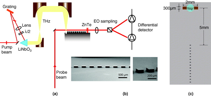
Figure 2. (a) Experimental THz time-domain spectroscopy system used to characterize the surface wave propagation in the silicon plasmonic waveguide. The THz waveforms are generated using a LiNbO3 crystal via optical rectification, and electrooptically sensed using a ZnTe crystal in close proximity to the waveguide. (b) Scanning electron micrographs showing a representative fabricated silicon waveguide structure. (c) Top-down diagram of experiment, showing the coupling groove and plasmonic waveguide. The blue region indicates the location and size of the normally incident THz input beam.
Download figure:
Standard image High-resolution imageAfter fabricating the silicon pillars, we used a similar photolithographic process to form a long, shallow groove oriented perpendicular to the start of the pillar array. The purpose of this groove is to break the symmetry of the planar surface, thereby allowing a normally incident terahertz wave to couple into the waveguide [29]. The coupling groove was 2 mm in length, 300 μm wide and etched to a depth of 50 μm, and it was separated from the start of the waveguide by 5 mm, as shown in figure 2(c).
Figure 2(a) depicts the terahertz time-domain spectroscopy system used to characterize the silicon waveguides. Pulses from a 1 kHz amplified Ti–sapphire laser system were split, using an 80:20 beamsplitter, into pump and probe pulses that were used to generate and detect the THz waveforms, respectively. The pump beam of tilted wavefront with an average fluence of 1.2 mJ per pulse, duration of 43 fs and a spot size of 3 mm was directed toward a LiNbO3 crystal in the orthogonal direction on the one side with cut at 63°. The THz is generated from the front end of the crystal via optical rectification [30]. The generated terahertz beam was collected and collimated using two off-axis parabolic mirrors. A third parabolic mirror was used to focus the THz beam at normal incidence onto the coupling groove. The groove was oriented such that the incident wave was linearly polarized in the direction perpendicular to the groove (parallel to the propagation axis of the waveguide)—a condition necessary for the excitation of plasmonic waves. By comparing the intensity measured after the coupling groove to that obtained by replacing the device with an off-axis parabolic mirror, we estimated input coupling efficiency to be 10%.
The THz waves were detected by using a 1 mm thick  ZnTe electrooptic crystal placed in close proximity to the surface of the waveguide. The probe beam, which is co-linear with the waveguide, was focused through the ZnTe crystal with a beam waist of 0.5 mm and pulse energy of 1 μJ. The probe beam was positioned approximately 0.5 mm above the pillar surface, thereby ensuring that there is no interaction with the substrate. The THz waveform is measured by varying the relative time delay between the pump and probe using a mechanical delay line, while electrooptically sampling the evanescent field of the plasmonic waveguide. To assess the degree of mode confinement, the ZnTe crystal and probe beam were displaced vertically while recording the THz field.
4. Results and discussion
Figure 3(a) shows the measured back-to-back THz spectrum (and the corresponding time-domain waveform, inset), obtained by bypassing the device. These measurements define the bandwidth capability of our measurement and were used as baseline for characterizing the device performance.
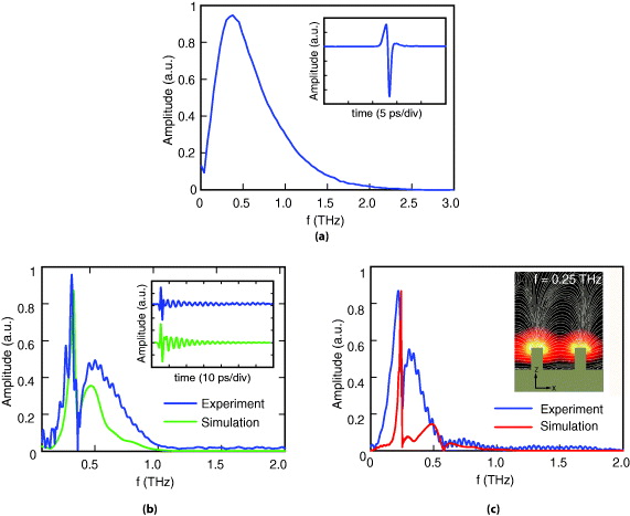
Figure 3. (a) Amplitude spectrum for input THz waveform. The inset shows the corresponding time domain spectrum. (b) Experimentally observed and numerically simulated waveguide transmission spectrum on a heavily doped silicon substrate patterned with sub-millimeter pillar of height h = 100 μm. The other parameters are: length l = 100 μm, width w = 200 μm, lattice constant p = 400 μm. The inset shows the corresponding time domain spectrum. (c) Frequency domain spectrum from simulation and experiment for the case when height h = 200 μm, while other parameters are same as figure (b). The inset shows the electric field profile and lines at the anti-resonant frequency i.e. 0.25 THz of fundamental resonant mode.
Download figure:
Standard image High-resolution imageFigure 3(b) shows the THz spectrum and time-domain waveform (inset) measured after a propagation distance of 50 mm along the surface of an array of silicon pillars. The pillars had a height h = 100 μm. The green curves illustrate the corresponding numerical simulation, which was obtained using the finite-element time-domain method. The measured back-to-back time-domain signal from figure 3(a) was used as the input signal in the numerical simulations. Figure 3(c) illustrates similar measurements obtained with a pillar height of 200 μm, with all other parameters identical to those of (b).
The numerical simulations and experiments are in agreement across the range of frequencies measured. The time-domain traces exhibit an oscillating transient characteristic that is associated with a spectral resonance of the structure. The corresponding spectra show a null at this resonance frequency, and the frequency of this null is well-matched between simulation and experiment. To illustrate the nature of this resonance, the inset to figure 3(c) shows the simulated field pattern calculated at the null frequency of 0.25 THz, evaluated in the cross-sectional plane at the center of the waveguide. At the resonant frequency, the fields are observed to be highly localized around the pillars, while at other frequencies the fields are poorly confined. One may note that there is small discrepancy between measurements and simulations above the resonant frequency. We believe this is because the mesh size in the numerical simulations in figure 3 was chosen to be approximately 40 μm, which is sufficient to model the behavior at lower THz frequencies, but can lead to quantization errors at higher frequencies.
The observed resonant frequency is also well-matched to the calculated frequency at the first Brillouin zone boundary. The group velocity approaches zero at the Brillouin edge, indicative of a standing wave, as expected for a resonant structure. As shown in figure 1(b) the Brillouin edge was calculated to occur at 0.35 and 0.25 THz for the 100 and 200 μm tall pillars waveguides, respectively. These values correspond to the null-frequencies observed in figures 3(b) and (c), respectively.
García-Vidal et al [8] recently reported an analytical theory to describe surface electromagnetic modes in a corrugated conducting surface. If one neglects diffraction effects, the dispersion relation of a 1D grating corrugation may be approximated as
where kx is the wave number in the direction of propagation, k0 ≡ 2πf/c is the free space wave number, h is the height of the corrugation and l/p describes the duty cycle of the corrugation. The first Brillouin boundary is considered by setting kx = π/p in equation (1) and solving for the corresponding frequency f. Using the dimensions of the 100 μm tall pillars, the analytical theory predicts a resonant frequency of 0.35 THz, in perfect agreement with experimental observations. We see similar agreement for other heights, as summarized in figure 4, which plots the experimentally measured null frequencies (filled blue circles), numerically simulated null frequencies (green dots) and analytically determined frequencies predicted from equation (1) (red curve). While the analytical theory was developed to describe a 1D array of linear grooves, it is remarkable how well it also describes the 1D pillar arrays considered here, which have a finite transverse width of w = 200 μm.
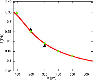
Figure 4. Variation of anti-resonant frequencies with the heights of the pillars on the heavily doped p-type silicon surface. The black triangles correspond to the experimentally observed values, while the green dots corresponds to the numerical simulations. The red curve represents the theoretical model with the following parameters: l = 100 μm, w = 200 μm and lattice constant p = 400 μm, and shows excellent agreement with the measurements and simulations.
Download figure:
Standard image High-resolution imageFurther, we study the effect of change of periodicity p on the resonance frequency of the fundamental mode. We fabricated a second set of devices with periodicity p = 300 μm and all other parameters held the same as in figure 3(b). The effect of periodicity is shown in figure 5(a). The blue trace shows the experimentally obtained transmission spectra for the periodicity p = 300 μm while the green trace corresponds to p = 400 μm. We observe that the periodicity plays an important role in defining the resonant frequency of the mode, as expected from the analytical model. This behavior is contrary what is observed for the periodic hole arrays, discussed in earlier papers [20], where the resonant frequency depends exclusively on the dimensions of the hole in a conducting plate. One may note that a decrease in the periodicity leads to a redshift in the frequency of the resonant.
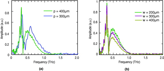
Figure 5. (a) Measured waveguide transmission spectra for periodicity p = 300 and 400 μm. The other parameters are: width w = 200 μm, length l = 200 μm and height h = 100 μm. The change in the periodicity influence the resonant mode behavior with other parameters constant. (b) Measured waveguide transmission spectra for different values of width w with all other parameters unchanged. The other parameters are: l = 100 μm, lattice constant p = 400 μm and height h = 100 μm.
Download figure:
Standard image High-resolution imageNext, we experimentally studied the effect of change of pillars width on the anti-resonant frequency of the fundamental mode. Waveguide structures with different widths w = 200, 300 and 400 μm were fabricated with fixed values of other parameters: l = 200 μm, p = 400 μm and h = 100 μm. The time domain spectra were Fourier transformed and results are shown in figure 5(b). We note that the null-frequencies were observed to not depend on the width w for all of the cases considered. Numerical simulations revealed that for 100 μm tall pillars, the structure provides the tightest transverse confinement for waveguide widths from 200–400 μm, and the confinement vanishes when the width is reduced below 75 μm.
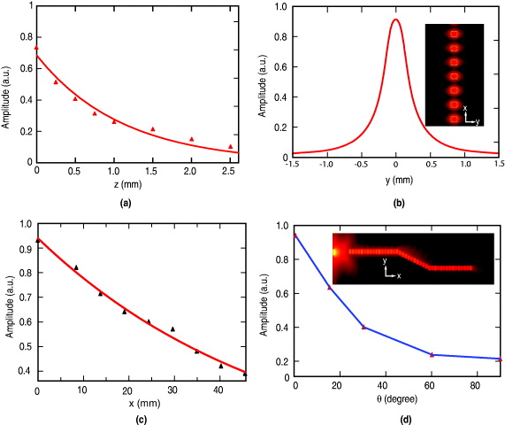
We next consider some key properties of the periodic silicon pillar structure that are relevant for waveguide applications. The degree of confinement of the mode in the transverse directions is an important waveguide property that was studied both experimentally and numerically. The vertical confinement was experimentally investigated by translating the electrooptic detection crystal (with the associated probe laser beam) away from the surface, while measuring the received terahertz temporal waveform at each position. Figure 6(a) plots the measured peak spectral amplitude as a function of the distance from the surface, along with an exponential fit, which reveals a 1/e length of approximately 1.1 mm.
Figure 6. (a) Peak spectral amplitude versus position of the electrooptic sensor above the surface. The solid curve shows an exponential fit, and the symbols indicate experimental measurements. (b) Simulated field profile of the waveguide, showing the degree of transverse confinement. (c) Measured wave amplitude as a function of propagation distance, along with exponential fit showing 1/e decay length of 5 cm. (d) Calculated bending loss for two successive angle bends, as a function of the bend angle. (Inset: calculated fields for a bend angle of 30°.)
Download figure:
Standard image High-resolution image
The horizontal confinement of the resonant mode was estimated by finite-difference time-domain simulation. Figure 6(b) plots the calculated field amplitude as a function of the transverse coordinate y for a pillar width of 200 μm, which shows a full-width at half-maximum of approximately 450 μm.
The attenuation along the direction of propagation was experimentally characterized by translating the electrooptic detection crystal in the x direction. Figure 6(c) plots the spectral amplitude as a function of distance, along with an exponential fit, which reveals a 1/e propagation length of 5 cm.
One of the key advantages afforded by a fully confined waveguide is the ability to direct electromagnetic radiation along a non-straight path. We investigate this possibility by numerically simulating the wave propagation through two successive angle bends. Figure 6(d) plots the numerically determined field attenuation factor as a function of the bend angle θ. The inset shows the numerically calculated wave amplitude at a resonant frequency of 0.36 THz for a wave traversing such a structure with an angle of 30°. The attenuation of this structure was estimated to be 7.5 dB compared with the straight waveguide of same length. For comparison, a right-angle bend (not shown) exhibits a significantly higher loss of 13.5 dB.
5. Conclusion
In summary, we experimentally and numerically discuss the terahertz surface plasmon polariton propagation on a heavily p-doped silicon surface structured with pillars. The pillars are fabricated using deep reactive ion etching of a photo-lithographically patterned silicon surface. Using terahertz time domain spectroscopy, we demonstrate that the fabricated patterns lead to the tightly confined resonant surface modes whose properties depends upon size and period of the pillars. A simple 1D analytical model [8] is found to accurately describe the dispersion relation and resonant modes of the structure, even for small waveguide widths. Numerical simulations validate the experimental observations, and further reveal the transverse confinement of the wave and three-dimensional waveguiding properties of the structure. The plasmonic structure presented here is a promising candidate for the constructure of future THz devices on silicon.
Acknowledgments
This work was sponsored by the Office of Naval Research, through the University of Maryland Center for Applied Electromagnetics (grant no. N000140911190) with the support of the Maryland NanoCenter and its NispLab and FabLab.