


Abstract
A simple chemical bath deposition method was employed in depositing nickel oxide films at different deposition times and afterwards they were spin-coated on by an already synthesized perovskite solar cell in an inverted planar architecture via a one-step spin-coating method. SEM results show nested and large compact clusters of oval-shaped grains while the EDX analysis confirmed the elemental composition of nickel and oxygen in the deposited films. The XRD results reveal an amorphous nature and a crystalline nature respectively for nickel oxide films without and with perovskite spin-coated on the surface. The optical results show good optical properties with a band gap energy ranging from 2.90 eV to 3.30 eV. The interfacial charge transport and recombination behaviour of the deposited films have been investigated with good electrochemical properties recorded. The obtained results on the inclusion of nickel oxide as a hole transport material makes it a good material in the production of highly efficient perovskite devices.
Export citation and abstract BibTeX RIS
1. Introduction
Nickel oxide (NiO) has octahedral sites with a rock-salt like cubic structure [1]. NiO is a p-type semiconductor [2] which can be stoichiometric or non-stoichiometric [3–5]. Some literatures have revealed a high hole transporting property of nickel oxide films deposited by various techniques [1, 6, 7]. Several reasons such as low cost, quick reproducibility etc have prompted research interest towards incorporating nickel oxide as a hole transporting material in perovskite solar cell devices (PSCs) like organic-inorganic hybrid lead halide [1, 8]. NiO films can be easily deposited over a large area and on any substrate to produce flexible solar cell devices [5]. The minimal conduction band of NiO is higher than that of perovskites while the maximal valence band of NiO corresponds exactly to that of perovskite materials [6, 9]. Nickel oxide can be used as a window material in inverted planar PSCs (see figure 1) because it has good visible light transparency owing to its wide band gap (3.4 eV to 4.0 eV) [10]. Nickel oxide amongst other hole transport materials like spiro-OmeTAd [11], copper (I) oxide (CuO) and copper (II) oxide (Cu2O) [12], poly3-hexylthiophene-2, 5-diyl (P3HT) [11], N, N-di-p-methoxyphenylamine [13], copper (1) iodide (CuI) [14], has proven more efficient as a hole transport material. NiO films have been synthesised as a hole transport layer (HTL) in PSCs using several methods such as simple solution process or chemical bath deposition (CBD) [15–18], sol-gel method [19–22], hydrothermal method [23], pulsed laser deposition (PLD) [24–26], sputtering technique [4, 27–30], successive ionic layer adsorption and reaction (SILAR) [17], electro-deposition method [31] etc The simple solution method widens the modulating features and application areas of the deposited NiO film [31].
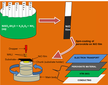
Figure 1. Sketch of the deposition techniques employed linked with a schematic on inverted planar perovskite architecture.
Download figure:
Standard image High-resolution imageOrganic-inorganic hybrid lead halides have gained tremendous research interest owing to their increasing efficiencies that have exceeded 21% in recent times [32–34]. The high efficiency obtainable depends on the band gap energy of the absorbing material [32]. Kojima et al initialised the use of perovskite materials as a light harvester [32]. Perovskite materials have wide spectra of light absorption, high absorption coefficient, several architectures obtainable from the device, ambipolar diffusion, high coefficient of extinction, increased length of diffusion and high mobility of the charge carriers [35–38]. These features have increased research interest in the perovskite research area. Perovskite solar cells can be fabricated in the form of a regular planar [36, 39, 40], inverted planar [1, 41, 42], mesoscopic [7, 43] and mesoporous [44] architectures. An inverted planar perovskite architecture as illustrated in figure 1 has the conducting substrate at the bottom with the perovskite material deposited on top of the hole transport material (HTM). Inverted planar architecture amongst other perovskite architectures has proven successful as it increases the magnitude of light harvested by the perovskite material; thereby producing a high power conversion efficiency (PCE) of the perovskite device [1, 45, 46].
Han et al studied the growth mechanism of nickel oxide thin films by room-temperature chemical bath deposition. This can be achieved by mixing 40 ml of 1 M nickel sulfate, 30 ml of 0.25 M potassium persulfate and 10 ml of aqueous ammonia and annealing at 500 °C. An optical band gap of 3.5 eV with cellular-like uniform grained morphology was obtained [18]. Xia et al studied the electrochromic properties of NiO thin films prepared by CBD method after annealing the films at 300 °C and using 1 M potassium hydroxide (KOH) as an electrolyte. The deposited films recorded a maximum transmittance of 82% [47]. Sun et al fabricated an inverted perovskite solar cell with a chemical bath deposited NiO scaffold as a hole transport layer. The optimised devices achieved 85% fill factor, 16.7% efficiency and a Fermi energy of −4.7 eV [48]. Zhu et al developed an inverted planar perovskite solar cell using a sol-gel-processed NiO nanocrystal as the hole transport layer. The perovskite material was spin-coated in a two-step spin-coating process using N-N-dimethylformamide and isopropanol as solvents [49]. Liu et al synthesised NiO via a non-injection thermolysis method. The perovskite film was deposited on the NiO film using a two-step spin-coating method. Pinholes were observed from the surface morphology while the films maintained crystalline structures [50]. Having gone through literature, we discovered the need to have an in-depth study of the optical, morphological, structural and electrochemical properties of nickel oxide films and nickel oxide films spin-coated with methylammonium lead iodide. Unlike previous literatures, one-step spin-coating method was adopted and diverse optical analyses have been carried out in this work in order to have an in-depth understanding of the optical features of the deposited films.
In this work, we synthesised nickel oxide films via a simple chemical bath deposition method. The nickel oxide films were prepared at molar concentrations different from those used in literature and annealed at lower temperatures. A pre-synthesised perovskite material (methylammonium lead iodide, CH3NH3PbI3) or MALI was spin-coated on the nickel oxide film in an inverted planar architecture at lower spin-coating speed and time. Modified parameters as compared to literature have been adopted in this study in order to obtain films with better features and application in perovskite devices. A comparison between the two sets of deposits: nickel oxide films with and without methylammonium lead iodide has been analysed. The morphological, structural, optical and electrochemical properties of the deposited films were studied using scanning electron microscopy (SEM), x-ray diffractometer (XRD), UV–vis spectroscopy and a 3-electrode potentiostat respectively. Extensive studies were done on the interfacial charge transport and recombination behaviours between the NiO and the perovskite.
2. Experimental details
2.1. Synthesis of NiOx films
Fluorine-doped tin oxide (FTO) and stainless steel (SS) substrates were washed with detergent and distilled water; ultrasonicated for 30 min, rinsed with acetone and dried in a hot air sterilizing cabinet at 60 °C for 30 min. The precursor for the NiO film was prepared by mixing 20 ml of 1 M nickel tetraoxosulphate (vi) hexahydrate (NiSO4.6H2O) with 60 ml of 0.25 M potassium persulfate (K2S2O8). 20 ml of aqueous ammonia was added to the solution and stirred properly until a color change from light green to ink blue was observed. Chemical bath deposition method (CBD) was used for the deposition of the nickel oxide film for 10, 20, 30, 40 and 50 min respectively on FTO and SS substrates respectively as shown in figure 1. Black deposits on the substrates were seen after rinsing in distilled water and drying at room temperature as seen in figure 1. The films were heated at 200 °C for 30 min to transform the hydroxide phase to the oxide phase of the nickel oxide films.
2.2. Preparation of the perovskite material-CH3NH3PbI3 or MALI
Pre-synthesised methylammonium lead iodide was purchased and used for this work. 150 μm of the MALI was dissolved in a beaker containing dimethylformamide (DMF) and dimethyl sulfoxide (DMSO) as additives/solvents and stirred properly.
2.3. Deposition of perovskite material on NiO films
A micropipette was used to drop 10 ml of the dissolved perovskite material on the nickel oxide film surface in an inverted planar architecture. A spin-coating technique as illustrated in figure 1 was employed in the deposition process at 400 rev/s for 60 s using a spin-coating machine on each NiO film in a one-step spin-coating process. Low spin-coating time was adopted and maintained in order to study its effect on the film properties. The samples were all dried at 60 °C for 30 min.
2.4. Characterisation of the deposited films
The films morphologies were observed by Zeiss scanning electron microscope (SEM), the x-ray diffraction (XRD) patterns were recorded with a D8 advanced x-ray diffractometer at a scanning range of 10–100° (λ = 1.5406 Å), the optical properties were investigated using Shimadzu UV-1800 spectrophotometer, electrochemical properties were obtained using a Princeton Applied Research VersaSTAT potentiostat in a three-electrode electrochemical cell comprising NiO deposited films as working electrodes.
3. Results and discussion
3.1. Morphological studies
The morphology of materials especially those in the nano-scale is an important factor in understanding the bulk material properties [51]. This is because smaller replace by grains have a greater surface area to volume ratio than bigger grains. The morphological (surface features) properties of the deposited films and the effects of the deposition times on the surface morphologies were studied using a scanning electron microscope (SEM) which applies the technique of scanning electrons in a raster scan pattern on the film surface.
The SEM images for different deposition times reveal different surface morphologies of the nickel oxide films showing the effect of deposition time on the as-synthesised NiO films. Figure 2 shows brick-like crystals (after 10 min of deposition) which got gradually transformed into nest-like clumps on increased deposition time. The large brick sizes obtained after 10 min is necessary for light absorption and increased film performance. The nest-like images obtained at higher deposition times are characteristics of NiO as observed by Xia et al [47] although the images obtained from their experiments were not in clusters but had porous features. However, the transformation process from brick-like spikes to nest-like clusters could be due to the increased deposition time. Each cluster at higher deposition time could be seen as an interconnection of nanosheets which form a structure of networks that are similar to that obtained by Yin et al [52]. The porous surface nature of the films which enhances electrochemical performance could be due to the deposition method employed [53]. Porous films deposited by CBD method have also been reported by [54, 55], and [56]. The rough NiO aggregates formed on the surface allows the formation of an efficient interface junction with the perovskite material; thereby increasing the device efficiency [49]. The porosity of the NiO sample provides a large surface area for the films to interact with the perovskite films, increases the transmission of light through the films and enhances charge transport between the layers. The morphology of the NiO films showing a vertical growth of the nanofilms outward could be responsible for the continuous net-like structures seen [53].

Figure 2. SEM images of the NiO films deposited at different deposition times.
Download figure:
Standard image High-resolution imageThe SEM images of the methylammonium lead iodide (MALI) spin-coated on the nickel oxide films are shown in figure 3. Large lumps of film clusters on the substrate surface get gradually reduced in size with increasing deposition time. The observed clusters show highly porous NiO films which would enable holes to be efficiently trapped and transported. The NiO + MALI film deposited after 50 min shows distinct spikes emanating from the substrate surface unlike the morphologies obtained from those at lower deposition times. The spikes give the growth direction of the deposited MALI film on the NiO film surface.
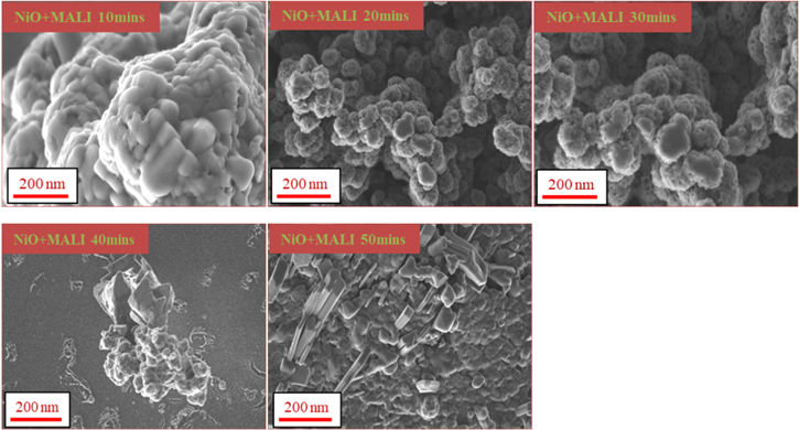
Figure 3. SEM images of the NiO films spin-coated with methylammonium lead iodide.
Download figure:
Standard image High-resolution image3.2. Structural studies
X-ray diffraction (XRD) method was used to confirm the structure of the deposited films. The XRD patterns of the nickel oxide films and those spin-coated with the perovskite compound are shown in figure S1 is available online at stacks.iop.org/ANSN/10/045009/mmedia. From the XRD patterns in figure S1, amorphous and crystalline structures were respectively obtained for the nickel oxide films synthesised at different deposition times and the nickel oxide films spin-coated with MALI respectively. Literatures have revealed amorphous [57] and crystalline [1, 44–46, 48, 51, 52, 58] structures of nickel oxide films. The diffraction peaks of the nickel oxide films spin-coated with MALI shows a crystalline structure. The shift in the peaks and lattice planes of the deposited methylammonium lead iodide could be due to the interaction of the nickel oxide/MALI films after deposition and formation of large brick of NiO/substrate as observed on the SEM image.
The lattice constants in table S1 were obtained from the most prominent peaks observed for all the samples using the mathematical relations in equations (1) and (2) [59]:

The increasing lattice constant values with increasing deposition time could be due to the decreasing oxygen pressure in the NiO films. The crystallite sizes, D were estimated using the Debye–Scherrer's formula in equation (2) [59]

where β is the full width at half-maximum, k = 0.94 is the shape factor, θ is the diffraction angle and λ is the wavelength of the XRD target. It can be observed from table S1 that the crystallite sizes of the samples increased with deposition time.
The dislocation density, δ [60] was calculated using the formula in equation (3):

Due to the non-homogenous nature of the films and crystal imperfections; the lattice strain, ε, was calculated using equation (4) [61]:

The inter-planar distance, d, which is the vertical spacing between parallel atomic planes in a crystal, was obtained from equation (5):

The Williamson-Hall's plots in figure S2 were also used to determine the crystallite sizes and the lattice strains of the samples obtainable from the slope of the fitted line and the intercept respectively. The tabular inset gives obtained plot parameters as shown in figure S2. The intercepts on the plots varied from 0.2181 to 0.3048.
Table S1 gives a summary of the crystal parameters obtained from the x-ray diffraction studies. The values for crystallite sizes, lattice constants, full width at half-maximum, lattice strain, interplanar distances and dislocation densities of the crystalline films have been respectively summarised in table S1. From table S1, the largest full width at half-maximum was recorded for the film deposited at 40 min while the film deposited at 30 min had the highest dislocation density.
3.3. Elemental analysis
Energy dispersive x-ray spectroscopy (EDS) was employed to confirm the elemental presence of elemental constituents in the deposited films. The major elements nickel (Ni) and oxygen (O) were confirmed as constituents of the deposited films as shown in figure S3.
Figure S3 shows the energy dispersive spectrum of the nickel oxide films deposited at 20 min and 50 min respectively. At high and low deposition times, the key elements were confirmed irrespective of the deposition time. The spectra displayed the quantitative composition of the elements deposited on the substrate surface in order of their different energies. The spectra confirmed the presence of the elements: nickel and oxygen in the deposited film. Other elements like silicon, calcium and potassium recorded could be attributed to the composition of the elements used in the substrate production and other laboratory equipment.
3.4. Optical results
The optical analyses of the deposited films have been investigated with a Shimadzu UV-1800 spectrophotometer. The absorbance graphs in figure 4 give information about how much of the incident light that gets absorbed by the deposited films.
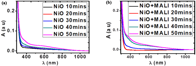
Figure 4. Plots of absorbance against wavelength for the deposited films at different deposition times.
Download figure:
Standard image High-resolution imageFigure 4 shows the UV–vis absorption measurement of the NiO films and the NiO/MALI films. The absorbance spectra of the NiO films and NiO/MALI were at different depositions in the range of 200–1100 nm. The films recorded maximum light absorption at about 300 nm in the ultraviolet region. The absorbance values of the films gradually decreased and attained a relatively constant value as it tends towards the visible and near-infrared regions. Moreover, the deviation in the absorbance is due to factors such as thickness and roughness on the NiO thin surface for different deposition times, which were not controlled during deposition. This is similar to the results obtained by [62–64]. The samples followed similar optical trends as observed in table 1. The absorbance of the deposited films increased as the thickness of the film and deposition time increased; thereby obeying Lambert's law.
Table 1. The summarised optical parameters obtained from the deposited films.
| Samples | A (%) | T (%) | R (%) | Eg (eV) | α (×105) cm−1 | n | Eu | ε1 | ε2 |
|---|---|---|---|---|---|---|---|---|---|
| NiO 10 min | 0.2 | 34.0 | 0.5 | 2.3 | 3.6 | 2.3 | 0.5 | 5.2 | 0.2 |
| NiO 20 min | 0.3 | 29.0 | 1.5 | 3.1 | 4.3 | 2.4 | 0.9 | 5.9 | 0.3 |
| NiO 30 min | 0.4 | 27.0 | 1.6 | 3.2 | 6.2 | 2.5 | 1.1 | 6.3 | 0.4 |
| NiO 40 min | 0.6 | 26.0 | 1.7 | 3.2 | 7.2 | 2.6 | 1.2 | 6.5 | 0.6 |
| NiO 50 min | 0.9 | 25.0 | 1.9 | 3.3 | 8.7 | 2.6 | 1.4 | 6.9 | 0.7 |
| NiO + MALI 10 min | 2.1 | 49.0 | 0.3 | 3.3 | 7.9 | 1.3 | 0.5 | 1.6 | 0.1 |
| NiO + MALI 20 min | 3.5 | 48.0 | 0.5 | 2.9 | 8.1 | 1.4 | 0.6 | 2.0 | 0.1 |
| NiO + MALI 30 min | 6.8 | 41.0 | 0.9 | 3.1 | 16.0 | 1.9 | 0.7 | 3.5 | 0.2 |
| NiO + MALI 40 min | 8.2 | 28.0 | 1.3 | 3.2 | 18.6 | 2.5 | 1.1 | 6.4 | 0.6 |
| NiO + MALI 50 min | 15.8 | 20.0 | 1.5 | 3.2 | 22.3 | 2.6 | 1.2 | 6.9 | 0.9 |
The amount of incident light transmitted into a material after absorption determines how much useful energy that would be obtainable from such material. High transmittance percentages of the deposited films as seen in figure 5 increase the efficiency of the solar cell device and make it a good candidate for optical materials.
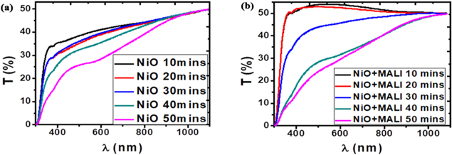
Figure 5. Graphs of transmittance against wavelength for the nickel oxide films synthesised at different deposition times and the nickel oxide films spin-coated with MALI.
Download figure:
Standard image High-resolution imageFigure 5 shows an increasing percentage of light transmission through the nickel oxide films deposited at different times with increasing wavelength. The films coated at lower deposition times transmitted more light because the films had less thickness than those deposited at higher deposition times; thereby giving room for more light penetration. Zhao et al obtained increased short-circuit current, carrier generation rate, reduced fill factor (due to increasing resistivity) as the thickness of the NiO film increased [65]. The transmittance of the NiO thin films increased from about 35% at 305 nm to a maximum value in the near-infrared region of the electromagnetic spectrum. High transmittance values have also been obtained by [41, 44, 46, 54, 66–69]. For the NiO thin films spin-coated with MALI, there was a gradual increase in the percentage of light transmission in the ultra-violet region until a maximum transmittance was recorded at about 500 nm wavelength. A little reduction at about 700 nm was observed in the transmittance and tends to a relatively constant value at about 1000 nm (towards the near-infrared region). The transmittance property of the deposited films improved upon spin-coating with methylammonium lead iodide and encourages the penetration of the spontaneously generated charge carriers and reduces recombination rate at the interfaces.
Reflectance plots give how much incident light gets reflected back upon incidence out of the material. A high reflectance percentage makes a material unfit for optical and solar cell usage. The reflectance (R) values of the films were obtained using the relationship in equation (6):

where A and T are the absorbance and the transmittance values of the deposited films respectively.
Figure S4 shows the reflectance graphs of the deposited films. The films deposited at different times experienced a slight increase in reflectance of light at about 310 nm. This slight increase was interrupted by a decline in the reflectance (seen as a curve) as it tends towards the infrared region at a relatively constant value. The deposited films could serve as good solar cell materials that would reflect very little of the incident solar radiation.
The absorption coefficient, α, of a material is the ratio of energy absorbed by a material to the energy incident upon the surface. The absorption coefficients of the deposited films in figure S5 were obtained using equation (7) [61]:

where A is the absorbance of the film and t is the film thickness.
The as-deposited films experienced a sharp decrease in the absorption coefficient values around their absorption edges as seen in figure S5. This sharp decrease occurred at slightly varying values of the absorption coefficient for all the films. The addition of the perovskite to the nickel oxide films shifted the maximum value of the absorption coefficient from the near-infrared region to the ultra-violet region of the electromagnetic spectrum. The absorption coefficient of the films increased with increasing deposition time and thickness as shown in table 1. The increased absorption coefficient of the nickel oxide films after spin-coating with perovskite is essential for the efficient absorption of holes from the perovskite layer by nickel oxide.
The extinction coefficient, k of a material measures how much light is scattered per unit volume. The formula for calculating the extinction coefficient is given by equation (8a):

From figure S6, maximum light scattering was obtained at about 300 nm and decreased as the wavelength tends obtained towards the near-infrared region. This decrease shows that much light would be absorbed by the deposited films at higher wavelength regions especially in the visible spectrum than would be scattered.
The optical conductivity, σ of a material tells how much light can be conducted by that material. The optical conductivities of the deposited films are shown in figure S7. Similar trends for the optical conductivity values were obtained for the films without and with the perovskite material. Maximum optical conductivity value was obtained for all the films at about 300 nm which makes the films good materials for optical devices in the ultraviolet region. A gradual decrease in the light conduction was obtained at higher wavelength regions. The film deposited at 50 min recorded the maximum light conduction as seen in figure S7.
Refractive index, n is a dimensionless quantity that gives how much of the incident light that gets propagated through the deposited films. Equation (8b) gives the refractive index formulae:

where k is the extinction coefficient and R is the reflectance of the deposited films.
The refractive index of the films increased with deposition times as shown in figure S8. The average refractive index of the nickel oxide films ranged from 2.25 to 2.63 while that for the NiO films spin-coated with the perovskite ranged from 1.18 to 2.58. The reduced refractive index values were attributed to the presence of the perovskite material spin-coated above the nickel oxide film. The reduced refractive indices make the NiO films integrable into perovskite solar cell devices and helps improve its stability. The maximum refractive index values were recorded in the visible region of the spectrum which is useful for solar cells [70].
The energy band gap plots of the deposited films measured in electron volts (eV) are shown in figure 6. The optical band gap energy of the deposited films was calculated using equation (9) [25]:

where α is the absorption coefficient, hν is the photon energy, A is a parameter that depends on the transition probability, h is Planck's constant, and the power n depends on the transition during the absorption process. n has values ranging from 1/2, 3/2, 2, and 3 for the direct allowed, direct forbidden, indirect allowed, and indirect forbidden transition respectively.
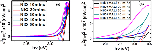
Figure 6. Plots of (αhν)2 versus photon energy to determine the energy band gaps of the as-deposited films at different deposition times.
Download figure:
Standard image High-resolution imageFrom the energy band curves in figure 6, the films without the MALI and those spin-coated with MALI exhibited similar band gap energies. The band gap energies range from 2.9 to 3.3 eV as shown in figure 6 and outlined numerically in table 1. The band gap energies of the films decreased with increasing deposition time. Introduction of the perovskite material caused a slight reduction in the band gap energies of the deposited films. This slight reduction is advantageous for thin films as their conduction bands are moved closer to the valence bands and less energy would be expelled by the carriers during band movement. Similar band gap energies have been obtained from some literature for nickel oxide films [18, 44, 58, 71]. With optical band gap tuning of the films, it would be useful in perovskite solar cell devices.
Urbach plot was gotten from the natural logarithm of the absorption coefficient and the photon energy as shown in figure S9. Urbach's empirical formula in equation (10) gives the exponential dependence of the absorption coefficient and the energy of the photons

where hν is the energy of the photon in eV,  is a constant; Eu is the Urbach energy that corresponds to the width of the exponential tail. Urbach energies ranging from 0.46 to 1.37 eV were obtained for the NiO films while Urbach energies ranging from 0.63 to 1.22 eV were obtained for the NiO + MALI films deposited at 10, 20, 30, 40 and 50 min respectively. These Urbach energies were gotten from the reciprocal values of the linear part of the plot in figure S9. The decrease in Urbach energy with decreasing deposition time could be due to an increased degree of orderliness in the deposited films.
The real and imaginary dielectric constants ε1 and ε2 respectively of the deposited films were calculated using the equations: ε1 = n2–k2 and ε2 = 2nk. Figures S10 (a) and (b) show the respective plots of the real and imaginary dielectric constants with respect to wavelength. Figure S10 (c) shows the change of the real dielectric constant with respect to wavelength-square. The values of the real and imaginary dielectric constants of the deposited films ranged from 1.55–6.88 and 0.01–0.92 respectively as shown in table 1. It can be observed that the dielectric constant values of the deposited films increased with deposition time. The low dielectric constant recorded upon spin-coating with the perovskite material is a good electric property which would enable the deposited films to withstand intense electric fields without breaking down.
3.5. Electrochemical studies
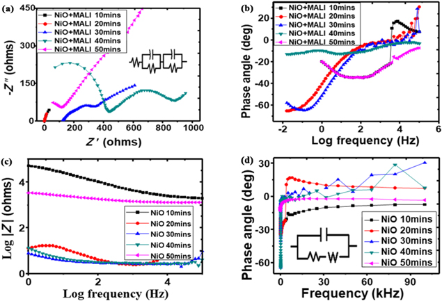
The electrochemical properties of the deposited NiO thin films were obtained using 1 M of potassium hydroxide (KOH) as electrolyte, Ag/AgCl electrodes as a counter electrode, the nickel oxide sample as a working electrode and carbon electrode as the counter electrode in a 3-electrode system. The porous nest-like nature of the deposited nickel oxide films enhanced the electrochemical performance because it provides a large surface reaction area and allows the electrolyte to penetrate into the bulk material and interact properly with the nickel oxide particles [54]. Electrochemical impedance spectroscopy (EIS) data were analyzed through the Nyquist and Bode plots which gave the charge transport and charge transfer properties of the films. The NiO films were evaluated in a frequency range of 10 mHz to 100 kHz. The Nyquist and Bode plots of the nickel oxide electrodes are as shown in figure 7.
Figure 7. (a)Nyquist plot (−Zell versus Zl) with a circuit inset R(CR)(CR), (b)–(d) Bode plots (phase angle versus log frequency), (log ∣Z∣ versus log frequency), (phase angle versus frequency) with an inset circuit element of the nickel oxide electrodes deposited at 10, 20, 30, 40 and 50 min respectively.
Download figure:
Standard image High-resolution image
To investigate the interfacial charge transport and recombination behaviours of devices, electrochemical impedance spectra of perovskite cells based on NiO HTM were measured. Figure 7(a) shows the Nyquist plots of the deposited films. A clear semicircle can be seen in relation to the charge transfer occurring at the FTO/HTL/Perovskite interfaces. The Nyquist plots in figure 7 are an indication that the ideal capacitors in parallel with the charge transfer resistors led to the formation of the semicircles seen. The beginning of the semicircle represents the solution resistance. The circuit inset: R(CR)(CR) in figure 7(a) was used to fit the NiO/perovskite films. The capacitors represent the movement of ions and charge storage in the electrochemical double layers. The charge transfer resistance (RCT) at the hole transport layer is evident from the high frequency semicircle [72]. The (C(RW)) circuit inserted in figure 7(d) was used to fit the deposited nickel oxide films with ZSimpWin software where RS, Cs and W designate the total ohmic resistance of the solution, capacitance of the double layer and the Warburg impedance respectively. The solution and charge transfer resistances recorded for the film deposited after 30 min were respectively 0.13 kΩ and 0.20 kΩ. The total ohmic resistance can be obtained from the three-electrode system while the capacitance is measured in Farads (F). The Warburg element gives the charge transfer resistance in the samples and the rate of diffusion of the ions in the electrolytes [73]. The above circuit gives the electrical resistances occurring between the samples and the electrode-electrolyte interface. The low resistances obtained are indicative of the efficient charge carrier transport occurring at the NiO/perovskite interface in the perovskite interface. Figures 7(b)–(d) show the Bode-phase plots. The diffusion and recombination of the carriers are represented in the high and low frequency regions respectively [45]. The low frequency region shows reduced carrier recombination due to better interfacial contact while the high frequency region shows efficient carrier diffusion from the perovskite layer to the hole transport layer. The reduced recombination rate encountered shows that when nickel oxide is incorporated into a perovskite device, the device carrier transport and performance would be increased.
Figure 7(d) shows a relatively constant phase angle with increasing frequency. At a constant frequency value, an increasing phase angle value was recorded. The NiO film and NiO/MALI films recorded the highest phase angle value and best electrochemical property. The NiO/MALI films at low deposition times exhibited better electrochemical and interfacial charge transfer properties. At high frequencies, the capacitance value reduces to approximately zero and the main contribution comes from the solution resistance while at low frequencies, the capacitors have very high impedance and all the current flows through the charge transfer resistors.
4. Conclusion
We successfully synthesised nickel oxide thin films at different deposition times using CBD method which is a simple and relatively inexpensive deposition technique. Inverted planar perovskite architecture was employed in depositing the perovskite material by a spin-coating method. Comparative analyses of the obtained results were studied as NiO proved to be a better hole transport material. SEM images of the nickel oxide films show nested and large compact clusters of oval-shaped grains. The structural properties of the deposited nickel oxide films were amorphous while those of MALI on NiO films were crystalline. EDX analysis confirmed the presence of the major elements: Ni and O. The deposited films exhibited similar and good optical properties. The energy band gaps of the deposited films ranged from 2.9 to 3.3 eV. Electrochemical impedance studies showed good electrochemical properties with good interfacial charge transport. The obtained results show that NiO would be an effective hole transport material which would enhance the performance and stability of perovskite solar cells. The deposited films find applications in light windows, optical devices and as an efficient hole transport material in perovskite devices.
Acknowledgments
FIE (90407830) cordially acknowledges UNISA for VRSP Fellowship award and also graciously acknowledge the grant by TETFUND under contract number TETF/DESS/UNN/NSUKKA/STI/VOL.I/B4.33, We thank the US Army Research Laboratory–Broad Agency Announcement (BAA) for the financial support given to this research (under contract number W911NF-12–1–0588). Also, we thank Engr. Emeka Okwuosa for the generous sponsorship of April 2014, July 2016 and July 2018 conferences/workshops on applications of nanotechnology to energy, health & environment and for providing some research facilities.