
Abstract
SnS2 nanoparticles have been synthesized using a mild hydrothermal method in the presence of the surfactant sodium dodecyl sulfate (SDS) at 180 °C for 12 h. Physical investigations were carried out to study their structure, size, morphology and optical properties. The x-ray diffraction (XRD) pattern of the as-prepared sample is indexed to the hexagonal phase of SnS2 and the particle size is 100 nm, which is further confirmed by transmission electron microscopy (TEM). The UV-visible spectrum shows that the absorption edge is blue shifted, and the band gap of the prepared SnS2 nanoparticles has been evaluated with UV-visible spectroscopy to be 3.54 eV, which is larger than the bulk SnS2 (∼2.44 eV). The anionic surfactant SDS plays a key role in the formation of the 3D sphere like SnS2 nanostructures. A probable reaction for the formation of nanocrystalline SnS2 nanoparticles is proposed.
Export citation and abstract BibTeX RIS

Content from this work may be used under the terms of the Creative Commons Attribution-NonCommercial-ShareAlike 3.0 licence. Any further distribution of this work must maintain attribution to the author(s) and the title of the work, journal citation and DOI.
1. Introduction
Nanomaterials have attracted great interest due to their intriguing properties, which are different from those of their corresponding bulk state. In the past few years, the synthesis and physical characterization of nanoscale semiconductors have aroused much interest [1–3]. Among the semiconductors, tin disulfide (SnS 2) has attracted attention due to its optical and electronic properties [4]. SnS 2, which is a layered semiconductor, belongs to a CdI 2-type structure with a bandgap of 2–3 eV [5, 6]. A broad bandgap leads to photoconductances [7, 8] and makes it possible for it to be a candidate in solar cells and opto-electronic devices [7–9]. It is also of interest in holographic recording systems and electrical switching [10]. Moreover, the bandgap of these nanoparticles is size dependent and therefore tunable [11]. As particle sizes become smaller, the ratio of the surface atoms to those in the interior increases, leading to a significant influence on the properties of the material surface [12]. A hexagonally close packed arrangement is found within the SnS2 layer and then the layers stack along the c-axis by weak Van der Waals forces. It exhibits different c parameters, which are integral numbers of the interlamellar spacing (5.899 Å) [13]. There are a large number of empty sites in their structure and hence they interest host lattices for intercalation [14, 15]. Up to now, well-defined SnS 2 nanostructures with different morphologies, such as fullerene-like nanoparticles, nanobelts, nanotubes and nanoflakes, have been synthesized successfully using a variety of methods, including lasing ablation, template-assisted solvothermal thief processes, and solvothermal and hydrothermal treatments [16–21]. Among these methods, hydrothermal is milder, simpler and less harmful to the environment than the other methods. SnS 2 has two advantages: (i) tin atoms may exist in a different oxidation state and various co-ordinations and (ii) sulfur atoms are greatly electronegative and are strongly polarizable.
In this work, SnS 2 nanoparticles were synthesized by anionic surfactant SDS, assisted under hydrothermal conditions, and its morphology and optical properties are discussed. The SDS plays a key role in the formation of the 3D sphere-like SnS 2 nanostructures.
2. Experimental procedure
In a typical synthesis, 0.50 g of the surfactant sodium dodecyl sulfate (SDS) was added to 64 ml of distilled water and stirred for 15 min. 0.35 g of SnCl 4·5H 2 O and 0.30 g of thiourea (H 2 NCSH 2) were added into the SDS aqueous solution. The mixtures were stirred vigorously for 30 min, transferred into a teflon-lined stainless-steel autoclave of 80 ml capacity, maintained at 180 °C for 12 h and allowed to cool to room temperature. The resulting yellow product was collected and washed several times using distilled water and absolute ethanol, and dried under a vacuum at 60 mmHg for 2 h.
The reaction of crystal waters of SnCl 4·5H 2 O with thiourea produced H 2 S. Then SnS 2 nanoparticles were obtained via the reaction of Sn +4 with H 2 S. The process could be as follows:
The synthesized sample was characterized by x-ray powder diffraction (XRD) using the Schimadzu model, XRD 6000 with CuKα radiation λ=1.5417 Å, at a scanning rate of 0.02 s −1 applied to record the patterns in the 2θ range 10°–80°. The UV-Vis absorption spectrum of the sample was recorded at room temperature by using a Varian cary5E spectrophotometer. Scanning electron microscope (SEM) analysis was carried out for the sample on a JEOL-JEM-3010 SEM. Photoluminescence (PL) measurements were carried out on a Fluoromax-4 spectrofluorometer with a Xe lamp as the excitation light source. Transmission electron microscopy (TEM) and energy dispersive x-ray spectrum analysis (EDAX) were carried out on the sample with a Philips model CM-20 by using accelerated voltage of 300 kV.
3. Result and discussion
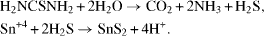
The XRD pattern of the as-prepared tin disulfide (SnS 2) is shown in figure 1. The intensities of the reflections are very small and hence the analysis of the crystalline phase of the sample is difficult. The low intensity XRD peaks indicate that the sample consists of coarsely fine grains (nanocrystalline/nor are they amorphous in nature). Sankapal et al [22] reported that CdS thin films deposited by the SILAR method, using cadmium acetate, were amorphous and/or nanocrystalline. In addition, the sample is randomly oriented, since the observed intensity of the peaks is less than the standard intensity. A matching of the observed and standard (hkl) planes confirmed that the samples are of SnS 2 having a hexagonal structure. All of the peaks in the XRD pattern can be readily indexed to a pure hexagonal phase of SnS 2 with a lattice constant a=3.649 Å and c=5.899 Å, which are in good agreement with the literature values (JCPDPS card no. 22–0951). The average particle size of the SnS2 calculated from the Scherer equation is about 100 nm. XRD did not show any contamination by other phases, such as tin sulfide or tin oxide. The energy dispersive x-ray spectrum of the SnS 2 nanoparticles is not shown here. It is found that tin and sulfur are present in almost atomic percentages (Sn:S=82.4:17.6). The result indicates that the as-synthesized SnS 2 nanoparticles are pure, which is in good agreement with the XRD result.
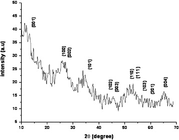
Figure 1 XRD pattern of the as-prepared SnS 2 sample.
Figure 2(a) shows the SEM image of the SnS2 sample with well-defined sphere-like morphology. SnS 2 samples were also prepared without using SDS at 180 °C for 12 h and it was observed that the particles formed undefined morphology, as shown in figure 2(b). In the case of figure 2(a), the SDS might bind on them regularly and effectively in 3D directions and reduce the surface energy, resulting in inactive sites for further self assembly. Therefore, well-defined spherical SnS 2 was formed. The anionic surfactant SDS plays a key role in the formation of the 3D sphere-like SnS 2 nanoparticles. Figure 3 represents the TEM image of the SnS 2 sample, which showed spherical nanoparticles of ∼100 nm, which is a similar result to that obtained by SEM and XRD analysis.
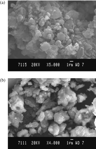
Figure 2 (a) SDS mediated SEM image of the SnS 2 sample. (b) Without SDS mediated SEM image of the SnS 2 sample.
Figure 3 TEM image of the SnS 2 sample.
Figure 4 shows the UV-Vis absorption spectrum of SnS 2 nanoparticles. The bandgap is found to be particle size dependent and increases with decreasing particle size. The absorption edge will shift to a higher energy concomitantly. The absorption edge is observed at 350 nm, which clearly indicates a blue shift from the bulk SnS 2 (∼507 nm). The corresponding bandgap energy (E g ) can be calculated to be 3.54 eV, which is larger than that of the bulk SnS 2 (∼244 nm) [5, 6].
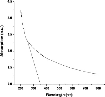
Figure 4 UV-Vis absorption spectrum of SnS 2 sample.
Figure 5 shows the emission spectrum for the SnS 2 nanoparticles taken at room temperature with an excitation wavelength of 300 nm. It exhibits two strong emission peaks at 410 nm and 490 nm, corresponding to blue emission. The SnS 2 nanoparticles exhibit a luminescence peak near the band emission at 410 nm and 490 nm (i.e. 3.02 eV and 2.53 eV) due to recombination of the bound excitons. Another possible explanation for the origin of this latter peak might be deep level emission due to impurities and native defects, such as interstitial tin atoms in SnS2 nanoparticles.
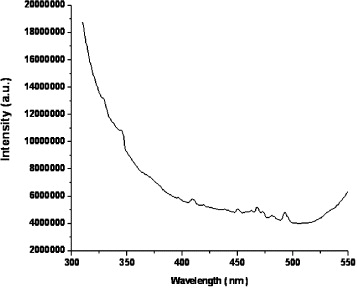
Figure 5 Emission spectrum of the SnS 2 nanoparticles.
4. Conclusion
We have reported the preparation of SnS2 nanoparticles by using a surfactant mediated method. The band gap of the prepared SnS2 nanoparticles has been evaluated with UV-Vis spectroscopy to be 3.54 eV, which is larger than the bulk SnS 2 (2.44 eV). The structural study of these samples reveals that they are nanocrystalline and/or amorphous in nature with a hexagonal crystal structure. Uniform spherical morphology is seen via SEM studies, while a ∼100 nm particle size was calculated from TEM studies. From the above experimental results, it can be concluded that the properties of nanocrystalline SnS 2, which is a good candidate for solar cell and optoelectronic devices, may be tuned.
Acknowledgment
The authors are grateful to the Tamilnadu State Council for Science and Technology for offering financial assistance to carry out this work.