

Abstract
Perovskite solar cells have been heavily investigated due to their unique properties such as high power conversion efficiency (PCE), low-cost fabrication by solution processes, high diffusion length, large absorption coefficient, and direct and tunable band gap. PCE of perovskite devices is strongly dependent on the absorber layer properties such as morphology, crystallinity, and compactness, which are required to be optimized. In this work, the CH3NH3PbI3 (170–480 nm) absorber layers with various methylammonium iodine (MAI) concentrations (7, 10, 20 and 40 mg ml−1) and perovskite solar cells with the fluorine-doped tin oxide (400 nm)/C-TiO2 (30 nm)/Meso-TiO2 (400 nm)/CH3NH3PbI3 (170–480 nm)/P3HT (30 nm)/Au (100 nm) structure were fabricated. A two-step solution process was used for deposition of the CH3NH3PbI3 absorber layers. The morphology, crystal structure, and optical properties of the perovskite layer grown on glass and also the photovoltaic properties of the fabricated solar cells were studied. The results obtained showed that by controlling the deposition conditions, due to the reduction in charge recombination, PCE enhancement of the perovskite solar cell (up to 11.6%) was accessible.
Export citation and abstract BibTeX RIS
Introduction
In the recent years, perovskite solar cells have been one of the most interesting scopes for researchers, due to their low cost and easy process ability, as evidenced by their unprecedented cell efficiency progress during the past several years. The organolead halide perovskite was first used in 2009 by Miyasaka in dye-sensitized solar cells as a dye [1]. The organometal halides have the general formula ABX3, where A is an organic cation (e.g.  ), B is a metallic ion (e.g. Pb2+, Sn2+), and X is a site occupied by a halogen ion (e.g. I−, Cl−, Br−) [2]. Perovskite CH3NH3PbI3 is a direct band gap (Eg) semi-conductor (Eg ∼ 1.55 eV at room temperature), which together with its unique properties such as a large diffusion length (∼0.1–1 μm), high mobility of the charge carriers (∼5 cm2 V−1 s−1), high optical absorption (∼105 cm−1), low cost, and simple processing deposition make it a suitable candidate for use as an absorber layer in the solar cells [3–5]. In order to use perovskite structures as the absorber layers in solar cells, an ideal morphology is a uniform and pinhole free layer, which prevents electron–hole recombination and amplifies photo-current. Thus the morphology, crystallinity, compactness, and composition of layers are required to be optimized. Several groups have shown that the perovskite morphologies such as the grain size and crystallinity highly affect the performance of solar cells [6, 7]. Highly efficient perovskite solar cells have been obtained using the perovskite grains as large as possible [8].
Moreover, the optical and electrical properties of the perovskite structures and, therefore, solar cell functionality, significantly depend upon the deposition conditions (e.g. molar ratio of precursors). Up to the present time, several researchers have tried to overcome these challenges using various chemical and physical deposition methods. The CH3NH3PbI3 layers can be prepared by one-step or two-step solution methods [9–12]. The two-step sequential solution method is a simple and more controllable deposition technique for fabricating highly efficient CH3NH3PbI3 solar cells [13]. In this procedure, first, a PbI2 solution is deposited on a substrate, and then by introducing methylammonium iodine (MAI) to isopropanol (IPA) and reaction with MAI, CH3NH3PbI3 is formed. Although in the two-step method sometimes some unconverted PbI2 remains in the system, the perovskite uniformity and grain size are more controllable [11]. Park et al have investigated the effect of MAI concentration on the morphology of perovskite grains to obtain highly efficient perovskite solar cells [14].
Further suitable electron selective materials such as TiO2, ZnO, and CdSe quantum dot/phenyl-C61 butyric acid methyl ester (PCBM) composite and appropriate hole selective materials such as Spiro-MeOTAD and Poly3hexylthiophene (P3HT) are required in order to have a good extraction of hole and electron generated carriers in the perovskite (PSK) layer which can lead to improvement of PSK solar cells efficiency [15].
In this work, a two-step spin coating method was used for the preparation of the CH3NH3PbI3 perovskite layers. Then the effect of MAI concentration on the structural and optical properties of the perovskite film and, therefore, power conversion efficiency (PCE) of the fabricated solar cell are reported.
Experimental details
For solar cell fabrication, fluorine-doped tin oxide (FTO) substrates were patterned by an HCl solution (2 M in deionized water) and Zn powder. Then the etched substrates were ultra-sonicated in a detergent, deionized water, acetone, ethanol, and isopropanol, each for 10 min, followed by drying at 100 °C, and subsequently treated by UV-ozone for 15 min. The cleaned FTO substrates were coated with a compact layer of TiO2 by spin coating of a mild acidic solution of tetraisopropyl orthotitanate in ethanol (2000 RPM for 30 s), followed by annealing at 500 °C for 30 min, treating with a 0.02 M TiCl4 solution in deionized water at 70 °C for 30 min, washing with deionized water, and drying at 100 °C. Then the substrates were annealed at 500 °C for 30 min. The mesoporous TiO2 layer was deposited on the TiO2 compact layer by spin coating (5000 RPM for 30 s) of the TiO2 paste containing 20 nm sized TiO2 nanoparticles diluted in ethanol (2:7 weight ratio), and immediately dried at 70 °C for 30 min. According to the literature, the efficient thickness of the mesoporous TiO2 layer is in the range of 400–600 nm [16]. By controlling the spin coating conditions and TiO2 nanoparticle precursor concentration, an efficient film thickness of 400 nm was obtained.
Similar to the compact layer, this layer was also annealed at 500 °C for 30 min. After mesoporous TiO2 deposition, it was treated with TiCl4 solution, as described for the compact layer. Then the CH3NH3PbI3 perovskite layer was deposited on the mesoporous TiO2 layer. A poly3-hexylthiophene)P3HT) layer (10 mg ml−1 in anhydrous chlorobenzene) was spin-coated on the perovskite layer at 1500 RPM for 40 s. Finally, a 100 nm thick Au cathode was deposited on it by a thermal evaporator with a shadow mask (Nanostructured Coatings Co, Iran).
In order to make the CH3NH3PbI3 absorber layer, the PbI2 precursor solution (1 M in anhydrous dimethylformamide (DMF)) was deposited on the mesoporous TiO2 substrate and also separately on a glass substrate for the perovskite layer characterization. Based on the efficient conditions introduced in the literature, this process was performed by a two-step spin coating at 3000 RPM for 5 s and 6500 RPM for 5 s, followed by heating at 40 °C for 3 min, and 100 °C for 5 min [17]. After thermal treatment of the layers, the CH3NH3I solution in anhydrous isopropanol alcohol (IPA) with various concentrations (7, 10, 20 and 40 mg ml−1) was dropped on the samples and rested for 20 s, then spun at 4000 RPM for 20 s, and subsequently heated at 100 °C for 5 min. The CH3NH3PbI3 layers with different MAI concentrations of 7, 10, 20 and 40 mg ml−1 were named as S1, S2, S3, and S4.
The structure of the layers was investigated using x-ray diffraction (XRD, Cu kα radiation, λ = 1.5406 Å, Bruker, AXS). The morphology and surface roughness of the samples were examined by a scanning electron microscope (SEM, VEGA//HITACHI S-4160 AND TESCAN) and an atomic force microscope (AFM, Arapasohesh, Iran). The optical properties of the samples were studied by UV–visible spectroscopy (1800 UV, Shimadzu).
The density current–voltage (J–V) characteristic of the fabricated solar cells based on the CH3NH3PbI3 absorber layer was measured using an Ivium Stat potentiostat (model: XRE, Netherlands) under a calibrated AM 1.5 solar simulator with a light intensity of 100 mW cm−2 (Sharif Solar 10-2, Iran). The thickness of the layers measured from the cross-sectional FESEM images and listed in table 1. To study the charge carrier recombination dynamics, the open circuit voltage decay analysis technique was used.
Table 1. Calculated average crystallite size, lattice parameter, unit cell volume, and thickness of perovskite layers made from various MAI concentrations.
| Lattice parameters (Å) | |||||
|---|---|---|---|---|---|
| Sample | Crystallite size (nm) | a = b | c | Cell volume (Å3) | Thickness (nm) |
| S1 | 50.2 | 8.91 | 12.52 | 993.94 | 170 |
| S2 | 44.8 | 8.86 | 12.67 | 994.59 | 230 |
| S3 | 46.7 | 8.82 | 12.78 | 994.19 | 290 |
| S4 | 38 | 8.91 | 12.61 | 1001.08 | 480 |
Results and discussion
The XRD patterns for the CH3NH3PbI3 perovskite samples (S1, S2, S3, and S4) are shown in figure 1. The observed diffraction peaks at 14.09°, 19.99°, 24.51°, 28.47°, 31.87°, 35.04°, 38.5°, 40.76° and 43.41° were assigned to the (110), (112), (202), (220), (310), (312), (322), (224) and (314) planes of the tetragonal perovskite structure [18]. The unconverted PbI2 peak can also be observed at 12.6° in the patterns; its intensity decreased as the concentration of MAI solution was increased. For the sample with a high concentration of MAI solution (S4), the observed PbI2 peak was very weak, which indicated that almost all the PbI2 were converted to the CH3NH3PbI3 perovskite. From the most intense (110) and (220) diffraction peaks, the average crystallite size of the layers (D) was estimated using the Sherrer equation (equation (1)):

In this equation, λ is the x-ray wavelength, β is the full width at half-maximum of the diffraction peak in radians, and  is the Bragg's angle.
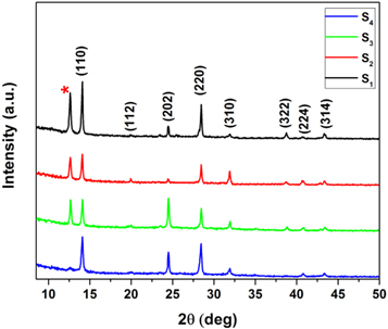
Figure 1. XRD patterns for CH3NH3PbI3 perovskite layers with different MAI concentrations grown on glass substrates S1 (7 mg ml−1), S2 (10 mg ml−1), S3 (20 mg ml−1), and S4 (40 mg ml−1). Star sign (*) represents PbI2 characteristic peak.
Download figure:
Standard image High-resolution imageBased on equations (2)–(4), the lattice parameters and unit cell volume of the perovskite layers were calculated using the (110) and (220) diffraction peaks:

in which n is the order of diffraction, λ is the x-ray wavelength, d is the lattice inter-planar spacing of the crystal, and  is the Bragg's angle


In equation (3), h, k, and l are the miller indices of the peaks, and a and c are the lattice parameters of the unit cell. The calculated results were summarized in table 1.
The results obtained show that although there is a PbI2 peak in sample S1, this sample has a better crystallinity than the other ones.
In order to evaluate the morphological structure of the samples, FESEM images were recorded for all samples and shown in figure 2. As it is obvious in these figures, particles are agglomerated with rather uniform distribution in all samples. Samples S2, S3, and S4 have nearly the same particle shapes and a uniform morphology. On the other hand, the S1 sample has a higher particle size and roughness. By comparison of the figures, we can see that with increase in the MAI concentration to more than 7 mg ml−1, the grain sizes significantly decrease from the average value of around 600 nm for the S1 sample to 150, 250 and 280 nm for the S2, S3 and S4, samples, respectively.
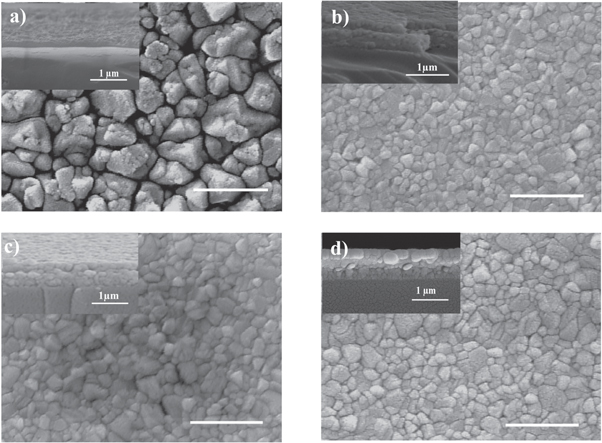
Figure 2. Top view FESEM images of CH3NH3PbI3 perovskite films (with cross-sectional image inset) with various MAI concentrations of (a) S1: 7 mg ml−1, (b) S2: 10 mg ml−1, (c) S3: 20 mg ml−1, and (d) S4: 40 mg ml−1 deposited on glass substrates; scale bars are 1 μm.
Download figure:
Standard image High-resolution imageThese results have demonstrated that proper concentration of MAI solution leads to the larger grain sizes and therefore, better crystal quality. Such a crystal grain size synthesized with the MAI concentration solution of 7 mg ml–1 may explained with a typical Ostwald ripening phenomenon. The MAI solution with low concentration (S1) could likely induce the Ostwald ripening mechanism for island coalescence during crystal growth [19]. In fact, due to atoms leave small islands more readily than larger islands, the newly germinated nuclei, which have radius less than the critical radius, are not much stable and may dissolve in the solution and accumulate over larger nuclei, which lead to the formation of larger grains. With increase in the MAI concentration, the Gibbs free energy could decrease, and the driving force for the nucleation increases. This phenomenon may lead to the formation of a critical nucleus with a small size. As a result, with a higher concentration of MAI solution (S2–S4 samples), a film with smaller grain size and lower porosity will form. In fact, due to for the S1 sample the growth was run by the low MAI concentration, when MAI solution dropped on PbI2 film and rested for 20 s (before spin), it was diffused in the PbI2 layer and the nuclei was sparsely distributed (localized nucleation) and then the larger grain of CH3NH3PbI3 is formed. But for the samples prepared by higher MAI concentration (S2, S3 and S4 samples), further crystal growth is inhibited, because nucleation and crystal growth are terminated immediately after adding MAI solution to PbI2 layer. By increasing MAI concentration from S1 to S4 samples, the nuclei density raise and then the growth of grain sizes decrease [6]. In figure 2, the insets show the cross-sectional image of the samples for estimating the average thickness of the layers.
However, it seems that an increase in the grain size for an MAI concentration higher than 10 mg ml−1 (S4 sample) is related to the other dominant mechanisms. On the other hand, we propose that with increase in the MAI concentration (by more than 10 mg ml−1), diffusion paths through the grain boundaries can form inside the PbI2 layer, which can cause more MAI molecules to reach the underlying PbI2 layer, and a more portion of PbI2 is converted to the CH3NH3PbI3 perovskite structure. The XRD patterns for the S4 sample (figure 1) is an evidence for this discussion that there is a very weak PbI2 peak indicating that almost the whole PbI2 is converted to the CH3NH3PbI3 perovskite structure.
The 2D and 3D topographic AFM images of the S1 and S4 samples are shown in figure 3. These images confirm the presence of pinholes in the perovskite films with a low MAI concentration (S1 sample). The surface roughness profile of the samples shows that the sample with a higher MAI concentration (S4) has a lower roughness.

Figure 3. (a), (b) 3D and (c), (d) 2D AFM images and (e), (f) surface roughness profiles of low (S1) and high (S4) concentration MAI perovskite films.
Download figure:
Standard image High-resolution imageIn order to investigate the optical properties of the perovskite thin films, the transmission spectra were measured in the range of 400–1100 nm and illustrated in figure 4(a). As shown in this figure, the S2 and S4 samples show the maximum and minimum transmission in the measured wavelength range, respectively. The higher/lower transmission of the S2/S4 sample could be due to the lower/higher thickness of this sample in comparison with the S3 and S4 samples. Although the S1 sample has the lowest thickness compared with the other samples, values of its transmission are lower than the S2 and S3 samples and higher than the S4 sample (table 1). This means that for this sample, other reasons such as grain size (d), morphology and surface roughness (higher porosity and roughness, see figures 2 and 3) should also be considered for this effect [20]. According to Rayleigh scattering (S) equation (5) that established for such low grain sizes in a few hundred nanometers ranges (compared to the visible light wavelength,  ):
):


Figure 4. (a) Transmittance, (b) absorption coefficient, and (c) Tauc's plots of perovskite films prepared from various MAI concentrations on glass substrates: S1, S2, S3, and S4 samples.
Download figure:
Standard image High-resolution imageWe expected the S1 sample (higher grain size than other samples) has lower transmittance. But transmittance of the S1 sample is higher than S4 sample which is likely because of much lower thickness of this sample than the S4 sample that may overcome the Rayleigh scattering phenomena [20–22].
Figure 4(b) shows the variation in the absorption coefficient (α) with photon energy for the perovskite thin films. The absorption coefficients were obtained from equation (6):

where A is the absorbance and t is the thickness of the layer. As expected, the values for the absorption coefficients of the samples were high. The absorption coefficient exceeded 2 × 105 cm−1 at higher photon energies. Accordingly, consistent with the transmittance spectra, S1 sample had the highest absorption coefficient, which is likely to be due to the larger grain sizes (lower carrier recombination) among these samples [20, 23]. Since stronger light absorption, and subsequently, more photo-generated carriers can be achieved from films contain larger grains [20]. To calculate the direct bandgap of the samples, the Tauc's equation was used:

where h is the Planck's constant, hυ is the incident photon energy, and A is an energy-independent constant. Then the direct band gaps of the layers were determined based on the extrapolated liner regression of  curves (figure 4(c)). The values obtained for the band gaps are listed in table 2. Although the absorption edge of the samples shows a little shift, the band gaps of all samples are nearly the same (about 1.550 eV), which is consistent with the reported values [24].
Table 2. Values for band gap and photo-voltaic parameters of fabricated solar cells based on CH3NH3PbI3 perovskite absorber layer prepared with various MAI concentrations.
| Samples (MAI concentration) | Eg (eV) | PCE (%) | Jsc (mA cm−2) | Voc (V) | FF (%) | Rs (Ω) | Rsh (Ω) |
|---|---|---|---|---|---|---|---|
| S1 (7 mg ml−1) | 1.556 | 11.6 | 20.6 | 0.92 | 0.62 | 6 | 297 |
| S2 (10 mg ml−1) | 1.552 | 2.7 | 13.5 | 0.56 | 0.35 | 25 | 190 |
| S3 (20 mg ml−1) | 1.553 | 7.1 | 14.8 | 0.93 | 0.51 | 12 | 850 |
| S4 (40 mg ml−1) | 1.560 | 8.2 | 16.9 | 0.86 | 0.57 | 9 | 773 |
In order to investigate the effects of different perovskite thin films synthesized by various MAI concentrations on the solar cell performance, four solar cells including the CH3NH3PbI3 absorber layers were fabricated. Figure 5 shows the schematic mesoporous device structure, cross-sectional image, and its energy band diagram. The TiO2 blocking layer (bl-TiO2) covers the etched FTO substrate. A uniform mesoporous TiO2 layer with a thickness of about 400 nm is deposited on bl-TiO2, and it is smoothly covered by a perovskite layer with a thickness of about 170–480 nm and then coated with P3HT as the hole transport layer (HTL). Then the Au cathode with a thickness of about 100 nm is evaporated on HTL.

Figure 5. (a) Schematic mesoporous device structure, (b) cross-section, and (c) energy band diagram of fabricated solar cells with CH3NH3PbI3 absorber layer.
Download figure:
Standard image High-resolution imageFigure 5(c) exhibits the energy levels of each device component and extraction of free charge carriers generated in the perovskite absorber layer under illumination by the electron and hole selective material.
The current density–voltage (J–V) characteristics curves of fabricated solar cells are shown in figure 6. The parameters extracted from the J–V curves such as PCE, fill factor (FF), short circuit-current density (Jsc), series resistance (Rs), shunt resistance (Rsh), and open-circuit voltage (Voc) were summarized in table 2. PCE and FF were obtained from equations (8) and (9):


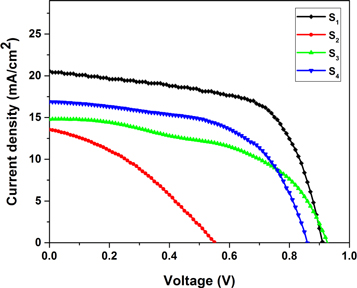
Figure 6. J–V curves for fabricated solar cells based on CH3NH3PbI3 perovskite layers with various MAI concentrations.
Download figure:
Standard image High-resolution imageRs and Rsh were measured from the slope of the J–V curves of solar cells at the Jsc and Voc points of the curves. The best photoelectrical parameters were recorded for the solar cell fabricated to the S1 absorber layer; they were consistent with the absorption coefficient (figure 4(b)). The results obtained show that the solar cell prepared from the absorber layer with a low MAI concentration (S1) has the highest efficiency of 11.6%. This may be attributed to the large grain size and appropriate cover of the mesoporous TiO2 layer, which prevent shunt path and efficient recombination of charge carriers in the layer, and also the beneficial effect of some residual PbI2 in the absorber layer of the device S1 [25]. As reported, the presence of excess PbI2 can improve crystallization of the perovskite layer by reducing the lattice strain [26]. As explained, the S1 sample has a significantly larger grain size, which causes the reduction of grain boundaries, leading to a lower carrier recombination rate and a higher PCE.
The solar cell fabricated with the S2 layer has the worst photo-electrical parameters, which may be due to a high recombination carrier in this layer. Since this sample has the lowest grains and light absorption and the highest grain boundaries that lead to high recombination of charge carriers.
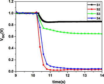
In order to study the charge carrier recombination dynamics in the fabricated devices with various MAI concentrations, the open-circuit voltage decay analysis was carried out. Figure 7 shows the normalized Voc decay curves for each solar cell. As shown in this figure, a fast drop in the photo-voltage occurs in devices based on the S2 and S4 layers after turning the light off. Among these devices, photo-voltage of the S1 device decay is slower than the other samples. The observed trend can be attributed to the presence of grain boundaries and defects. The defects in the crystal structure are generally expected to decrease the lifetime of the photo-generated charge carriers in the absorber as additional recombination pathways speed-up the loss of excess carriers [27]. Also the interfaces could introduce trap states for charge transport that influence the recombination dynamics. If there are a significant number of shallow trap states for both electrons and holes, long living charge carriers may be expected due to a slow de-trapping process. Therefore, the fast and slow voltage decay regime would correspond to the recombination of free charges and the recombination of the slowly de-trapped carriers, respectively. On the other hand, in contrast to the shallow trap states, if the number of deep trap states that act as recombination centers increases, the carrier lifetime decreases. Therefore, by comparing the results, for the solar cell based on the S1 absorber layer, due to higher grain sizes, may shallow trap states are more active than in other devices. On the other hand, a fast drop in the photo-voltage occurs in devices based on the S2 and S4 layers (lower grain size) after turning the light off. This may be due to higher accumulation of charge carriers at the interface which may lead to rapid carrier recombination. Moreover, in devices based on the S1 and S3 layers, the electrostatic (ES) potential due to accumulation of slow mobile ion charges at both sides of the interface may cause dramatically long decay times. This additional ES potential for devices based on the S2 and S4 layers is significantly lower than that of devices based on the S1 and S3 samples as a result of the higher recombination rate. This ES goes beyond the natural built-in voltage of the interface under illumination and it somewhat compensates for the higher recombination during open-circuit conditions [28]. As a result of this phenomenon, we can see an additional photovoltage in photo-voltage decay curves which still has not reached zero during 14 s (figure 7). The higher open circuit voltage of devices based on the S1 and S3 samples (∼0.93 V) compared to that for other devices (0.56 and 0.86 V) could be due to the much higher additional ES in devices based on the S1 and S3 layers. However, one may note that from the given set of experiments, it is difficult to identify the real origin of the increased charge carrier lifetime for the fabricated solar cells.
Figure 7. Normalized photo-voltage decay of fabricated devices based on CH3NH3PbI3 perovskite layer: S1 (7 mg ml–1), S2 (10 mg ml−1), S3 (20 mg ml−1), S4 (40 mg ml−1).
Download figure:
Standard image High-resolution image
Conclusion
In this work, the morphological, structural, optical, and photo-voltaic properties of the perovskite layers and fabricated solar cell based on the perovskite layers [(FTO(400 nm)/C-TiO2 (30 nm)/Meso-TiO2 (400 nm)/CH3NH3PbI3 (170–480 nm)/P3HT (30 nm)/Au (100 nm)] were studied. A two-step spin coating method was used for the preparation of the CH3NH3PbI3 perovskite layers with various MAI concentrations (7, 10, 20 and 40 mg ml−1). The band gaps of all samples were about 1.550 eV. Moreover, the results obtained showed that the sample prepared by a high concentration of precursor solutions (40 mg ml−1) had a pure CH3NH3PbI3 perovskite structure and a lower surface roughness. However, in application to the absorber layer in solar cell devices, the sample prepared with a low concentration of precursor solutions (7 mg ml−1) had better photo-electrical properties. Because this sample has higher grain sizes and absorption that have significant effects on the photo-electrical properties of the solar cell device. The results obtained show that by controlling the deposition conditions, due to the reduction in charge recombination, PCE enhancement of the perovskite solar cell (up to 11.6%) is possible. In this work, a device with an absorber layer prepared from a low concentration of MAI solution (7 mg ml−1) was introduced as an efficient structure for the mesoporous perovskite solar cell.
Acknowledgements
The authors gratefully acknowledge the financial support of the Shahrood University of Technology and the equipment services from the Nano Optoelectronic Laboratory (NOPL) of the Tarbiat Modares University.