

Abstract
In this work, the application of RF power in stepped mode during the growth process of CdTe films deposited on glass substrates at room temperature and their structural, morphological, and optical properties were studied. The working pressure and deposition time during deposition were 10 mTorr and 120 min, respectively, meanwhile the RF power was gradually varied from 30 W to 40 W. For comparison and reference, CdTe films with 30 W and 40 W (fixed power values) were also deposited, which resulted amorphous. The x-ray diffraction results of the films prepared with stepped RF power were polycrystalline with cubic structure and (111) as preferential orientation. The crystallite size of films changes from 16.6 to 29.2 nm as the rate of the stepped RF power increases. Raman spectra show that intensity of peaks located at 123, 140 and 164 cm−1 increase with the increased rate of stepped RF power, as well as the rms-roughness and grain size values increase from 0.8 nm to 1.6 nm and from 62.8 nm to 92.1 nm, respectively. The UV–vis spectra show that the bandgap energy of the deposited CdTe films changes from 1.47 to 1.54 eV with the increased rate of stepped RF power. The obtained bandgap energy values of the CdTe films are adequate to be used as absorber material for photovoltaic applications into the ZnO/CdTe and CdS/CdTe solar cells.
Export citation and abstract BibTeX RIS
1. Introduction
The compound semiconductor materials have been widely used into several fields of materials science such as energy, biomedicine, and environment. Particularly, cadmium telluride (CdTe) is suitable for solar cells fabrication due to its important properties such as long-term performance stability [1], direct bandgap energy (1.45 eV) photovoltaic solar energy conversion [2], high absorbance [3], and a high absorption coefficient (>105 cm−1) in the visible range of the solar spectrum for thicknesses below 800 nm [4].
Several techniques have been reported for CdTe films deposition including electrodeposition [5], closed space sublimation [6], pulsed laser deposition [7], molecular beam epitaxy [8], successive ionic layer adsorption and reaction [9], vacuum evaporation [10], electron beam evaporation [11], RF sputtering [12], and spray pyrolysis [13]. Among these techniques, RF sputtering is an effective technique to obtain nanocrystalline films since it enables control of volume distribution and size of nanoparticles over a wide range of conditions, and is commonly used for CdTe films deposition. Since, the physical properties of CdTe films deposited by RF sputtering can be modified from the applied power value, substrate temperature, type and flux of used gas, chamber pressure, etc; such studies have been done on their structural, optical, and electrical properties. For example, Camacho-Espinosa et al [14] reported the structural and morphological characteristics of the CdTe films deposited by RF sputtering as a function of the substrate temperature (23 to 250 °C) using three deposition times (30, 60, and 90 min) with a RF-power value of 40 W. Choi et al [15] investigated the effects of the surface morphology and thickness uniformity on the electrical and optical properties of the CdTe films deposited on ITO/Corning glass substrates by RF sputtering with applied powers from 20 to 50 W and chamber pressures from 1 to 80 mTorr. These authors reported coalescence and increase of grain size when the substrate temperature increases. On the other hand, Lin et al [16] observed improved quality of the (002) hexagonal crystalline structure in aluminum nitride films deposited on silicon by sputtering in two stages, applying for each stage different power (1.5/2.0 kW) and deposition time (15/45 min).
In this work, CdTe films were deposited on glass substrates (at room temperature) by RF sputtering by using different stepped power. The applied RF powers for deposition are stepped in ascending and descending RF power values. In addition, CdTe films were deposited with fixed RF power (30 W and 40 W) for comparison and reference. The structural, morphological, and optical properties of the deposited CdTe films as a function of the applied RF power were investigated by x-ray diffraction (XRD), Raman spectroscopy, atomic force microscopy (AFM), scanning electron microscope (SEM), and UV–vis spectroscopy.
2. Experimental
The CdTe films were deposited by RF sputtering technique on Corning 7059 glass substrates of 10 × 10 mm2 and 1.0 mm-thick at room temperature. Before deposition, the substrates were ultrasonically cleaned with xylene (Sigma-Aldrich, 98.5%), acetone (Sigma-Aldrich, 99.9%), methanol (Sigma-Aldrich, 99.9%), and dried with air. A commercial CdTe target of 99.999% purity from Kurt J Lesker and one inch-diameter was used. The distance between target and substrate was about 50 mm. The base-pressure was of 2 × 10⁻⁵ Torr and the work pressure was manually fixed at 10 mTorr with argon gas of 99.999% purity by a needle valve. A pre-sputtering of 30 min was carried out for cleaning the target surface. As a reference, two groups of CdTe films were initially deposited by using fixed power values of 30 W and 40 W, during 120 min. Then, other groups of films were deposited by modulating the applied RF power in stepped stages during all the deposition time of 120 min as follows: initially, we apply 40 W during certain time; then, a stepped reduction until 30 W is achieved; finally, a new increment until 40 W is done. Such that a stepped RF power cycle (40 W → 30 W → 40 W) is generated. The steps of applied RF power (ΔP) during deposition were fixed at 2 W while the steps of time (Δt) were 10, 5, 2.5 and 1 min, such that the different rate of stepped RF power with time (ΔP/Δt) were of 0.2, 0.4, 0.8, and 2.0 W min−1, respectively. A detailed representation of the different applied power cycles during deposition of the CdTe films is shown in figure 1.
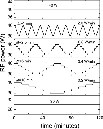
Figure 1. Different types of applied RF powers used for CdTe films deposition.
Download figure:
Standard image High-resolution imageGrazing-incidence x-ray diffraction patterns were obtained with a Bruker D8 Advanced diffractometer, using Cu Kα (λ = 1.5404 Å) radiation. The diffractograms were obtained at grazing angle of 1°, 2θ ranged from 20° to 70°, step size of 0.02°, and 45 kV and 45 mA conditions. Surface morphology of the CdTe films were discussed from the (1 × 1) μm2 images obtained with an atomic force microscope (AFM, Ambios universal) in tapping mode with a SiN cantilever coated with gold. The AFM images were obtained at a scan rate of 1 Hz with 256 × 256 pixels2 of resolution. The surface of the deposited films was also observed with a field emission scanning electron microscopy (FE-SEM, Jeol JSM-7600F). The Raman spectra of the films were recorded using a Raman spectrometer (Horiba LabRam HR) with a He-Ne laser (632.8 nm, wavelength) at 150 mW. The thickness of the films was measured with a Veeco Dektak 150 profilemeter and the optical transmission spectra were recorded with a Cary 5000 UV–vis-NIR spectrophotometer between 300 to 1500 nm of wavelength.
3. Results and discussions
The x-ray diffraction (XRD) patterns of the CdTe films deposited with fixed powers of 30 W and 40 W and with different rate of stepped RF power are shown in figure 2. From figure 2 can be observed that CdTe films deposited with fixed powers of 30 W and 40 W are amorphous. These results coincide with those reported by Ghorannevis et al [17] who attribute the absence of crystalline structure in the CdTe films to the fact that the applied RF power value is not enough for crystallization. On the other hand, samples deposited with different values of ΔP/Δt (0.2, 0.4, 0.8 and 2.0 W min−1) show to have crystalline structure with diffraction peaks at 2θ = 23.48°, 38.50°, and 46.17° corresponding to the (111), (220) and (311) cubic orientation, respectively (JCPDS file No. 15-0770). From these results, strong evidence from amorphous to cubic crystalline structure conversion is obtained. These results can be explained by the stepped RF power used during deposition, where improved electron mobility is promoted by the changes in kinetic energy of the adatoms sputtered on surface, which are required for obtaining films with high crystalline structure, as reported by Chan and Teo [18]. The CdTe films deposited with ΔP/Δt = 2.0 W min−1 show the higher diffraction intensity of the cubic (111) orientation. The XRD spectra of the CdTe films deposited with the ΔP/ΔΔt values of 0.2, 0.4, 0.8 and 2.0 W min−1 show mainly (111) cubic orientation, probably due by the increased diffusivity of atoms in the substrate, which allows easy orientation, given that (111) orientation requires lower surface energy than (220) and (311) orientations during the growth process, in accordance with Huimin et al [19].

Figure 2. XRD patterns of the CdTe films deposited at different ΔP/Δt values.
Download figure:
Standard image High-resolution image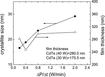
Figure 3. Crystallite size and mean thickness values of the CdTe films deposited at different ΔP/Δt values.
Download figure:
Standard image High-resolution imageThe crystallite size (d) of the CdTe films was estimate using the Debye–Scherrer equation [20]:

Where λ is the wavelength of the x-rays, B is the full-width at half-maximum and θ is the Bragg diffraction angle. The estimated crystallite size of the CdTe films deposited with ΔP/Δt values of 0.2, 0.4, 0.8 and 2.0 W min−1 increased from 16.6 to 29.2 nm (see figure 3). From figure 3, the CdTe films deposited with a ΔP/Δt = 2.0 W min−1 show the higher average crystallite size. The mean thickness value and deposition rate of the prepared CdTe films ranges from 175 to 303 nm and from 1.45 to 2.52 nm min−1, respectively. These values suggest that an increase of the rate of stepped RF power during the sputtering process results in an improved film crystallization which is attributed to an increase on the grain size.
Figure 4 shows the Raman spectra of the obtained CdTe samples. From figure 4(a), samples deposited with ΔP/Δt of 0.4, 0.8, and 2.0 W min−1 present vibrational modes at 123, 140 and 164 cm−1 position. The first peak corresponds to the A1 vibrational mode of Te, the second one to the overlapping of the TO phonon of CdTe and E symmetry of Te [21], and the third peak is related to the LO of CdTe. To perform a better analysis of the Raman spectra of the aforementioned samples, the observed peaks were adjusted with a Lorentzian function [22]. Figure 4(b) shows the fitting curves, where can be observed, in addition to the previous vibrational modes of the CdTe, the presence of two additional peaks: one at 150 cm−1 corresponding to the SO mode, and other at 180 cm−1, attributed to 2LO-SO mode.
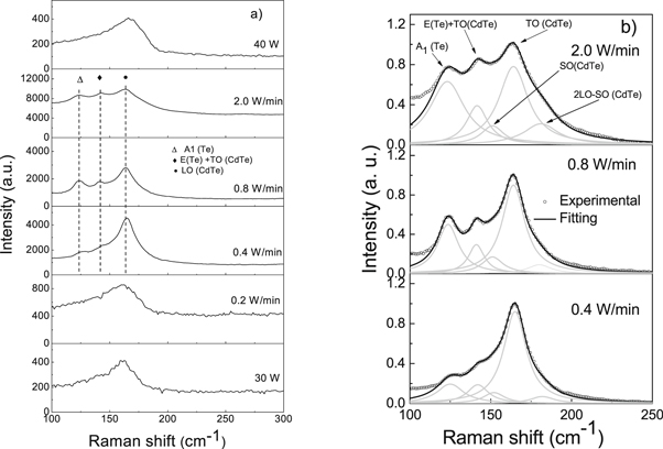
Figure 4. (a) Raman spectra of the CdTe films deposited at different RF power conditions, (b) fitting of the spatial correlation model of the samples deposited at different ΔP/Δt values (0.4, 0.8 and 2.0 W min−1).
Download figure:
Standard image High-resolution imageThe presence of these fitted peaks indicates a higher quality of the CdTe films as reported by Younghun et al [23]. On the other hand, the CdTe films deposited with constant power of 30 W and 40 W, and with ΔP/Δt = 0.2 W min−1, show the same LO phonon vibrational mode with a peak of low intensity which indicates the amorphous character of the films (poor crystallinity). Normally, the presence of the three peaks (A1, TO and LO) shows that these films suggest p-type electrical conductivity; while the only presence of the LO mode suggests an n-type electrical conductivity, according to [24]. From here, we assume that the CdTe films deposited with ΔP/Δt of 0.4, 0.8, and 2.0 W min−1 are of p-type.
The surface morphology evolution of the CdTe films as a function of the applied RF power is presented in figure 5 as obtained from AFM images (1 × 1 μm2). The CdTe film deposited with constant power of 40 W, shows larger and hemispherical grains with a mean diameter of 159 nm. On the other hand, the CdTe films deposited with different rate of stepped RF power presents very smaller, homogeneous size, and spherical grains with diameters between 63 and 91 nm, as is shown in figure 6. Finally, for samples deposited with constant power of 30 W, surface morphology does not have a well-defined geometry, maybe by the reduced energy of the atoms arrived on the substrate.

Figure 5. AFM images (1 × 1 μm2) of CdTe films deposited at different RF power conditions: (a) 40 W, (b) 0.2 W min−1, (c) 0.4 W min−1, (d) 0.8 W min−1, (e) 2.0 W min−1, and (f) 30 W.
Download figure:
Standard image High-resolution image
Figure 6. Grain size and rms-roughness values of the CdTe films deposited at different ΔP/Δt values.
Download figure:
Standard image High-resolution imageA plot of the estimated grain size and rms-roughness values of the CdTe films deposited at different ΔP/Δt values is shown in figure 6. For comparison, the values estimated for the CdTe films obtained with constant applied power are included in the inset of figure 6. An increment of the grain size with the increasing ΔP/Δt value is observed. Authors have reported that grain size depends on some factors as substrate temperature, magnetron size, film thickness, and type of substrate [25–28]. In our work, the grain size is strongly affected by the rate of stepped RF power used for CdTe deposition. From figure 6 can be observed that the rms-roughness of the CdTe films deposited with different ΔP/Δt values is found to be between 0.8 and 1.6 nm, these values are smaller than those obtained for samples deposited with constant power (3.3 nm for 30 W, and 14.6 nm for 40 W, respectively). Our reported values are minor than those reported by Islam et al [29] for sputtered-CdTe films deposited by at different substrates temperatures and a CdCl2 post-treatment. They reported roughness values between 20 and 30 nm for CdTe films with post-annealing and values between 10 to 25 nm for films with a CdCl2 treatment, where the decrease of film roughness indicates growth of grains size by the annealing temperature.
FE-SEM micrographs of the CdTe films deposited with constant power and different rate of stepped RF power are shown in figure 7. From figure 7(a), the CdTe films deposited with 40 W, present some larger and spherical grains with diameter of 160 nm, while for films deposited with 30 W (figure 7(f)) shows grains with diameter of 100 nm. In both cases, spherical grains located on surfaces composed of very smaller grains of CdTe can be observed. It is important to point out that larger grains are of CdTe as energy dispersive analysis (EDS) demonstrated. For the CdTe films deposited with different ΔP/Δt values, figures 7(b)–(e), coalescence of grains is observed on surface and grain diameters of 61, 68, 81, and 87 nm, respectively, were measured.
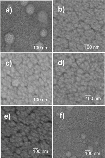
Figure 7. FE-SEM micrographs of CdTe films deposited at different applied power: (a) 40 W, (b) 0.2 W min−1, (c) 0.4 W min−1, (d) 0.8 W min−1, (e) 2.0 W min−1, and (f) 30 W.
Download figure:
Standard image High-resolution imageThe optical transmittance spectra of the CdTe films deposited at fixed 30 W and 40 W and different ΔP/Δt values were measured in the wavelength range of 300 to 1500 nm and are shown in figure 8(a). The CdTe films deposited with ΔP/Δt values are highly transparent in the near-infrared region and the optical transmittance varies from 70 to 90% in comparison with the films deposited with constant power (30 W and 40 W) which show transmittances lower than 60% at the same region.
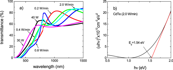
Figure 8. (a) Transmittance spectra of the CdTe films deposited at different conditions of RF power, (b) Tauc spectra of the CdTe films deposited with a ΔP/Δt value of 2.0 W min−1.
Download figure:
Standard image High-resolution imageThe absorbance of the films as a function of wavelength was analyzed to estimate the bandgap energy using the Tauc relation [30]:

Where α is the absorption coefficient, A is a constant, n is an integer number with n = 1 for a direct bandgap material, n = 4 for an indirect bandgap material, h is the Planck´s constant, ν is the frequency of the light, and Eg is the bandgap energy.
Figure 8(b), shows the estimated Eg = 1.54 eV for the CdTe film deposited with a ΔP/Δt = 2.0 W min−1. A similar procedure was used for estimating the bandgap energy for all the CdTe samples. The Eg values for the CdTe films deposited with constant power was 1.32 eV (30 W) and 1.45 eV (40 W), respectively. An increased Eg value from 1.47 to 1.54 eV was obtained for the CdTe films deposited when the ΔP/Δt value increases. The Eg value as a function of the rate of stepped RF power is shown in figure 9. The corresponding Eg bulk value for CdTe (Eg bulk = 1.45 eV) [2] is included (dashed-lines) as reference. Our estimated Eg values are in good concordance with the values reported by other authors. For example, Choi et al [15] estimated the bandgap energy between 1.41 to 1.45 eV for CdTe films deposited by sputtering technique. Espinosa et al [31] reported values in the range of 1.44 to 1.60 eV for CdTe films deposited by sputtering technique at different deposition pressures. An increase of the bandgap energy value from 1.47 to 1.51 eV for CdTe films deposited by sputtering technique with substrate temperatures from 50 to 300 °C was also reported by Kulkarni et al [32].

Figure 9. Bandgap energy values of the CdTe films deposited at different RF power conditions.
Download figure:
Standard image High-resolution image
4. Conclusions
CdTe thin films were deposited on glass substrates by RF sputtering technique by using constant applied RF power (30 W and 40 W) as well as different rates of stepped RF power. XRD results demonstrated that the deposited CdTe films with constant power are amorphous, but films deposited with different rates of stepped RF power are polycrystalline with a cubic (111) as mainly preferential orientation. Furthermore, by increasing the rate of stepped RF power, the crystallinity of the CdTe films improves. FE-SEM and AFM images confirmed that the average grain size increases when the rate of stepped RF power increases. The rms-roughness values of the CdTe films deposited under different rate of stepped RF power were lower in comparison with the films deposited at constant RF power. The UV–vis spectroscopy analysis revealed that the bandgap energy increases from 1.47 to 1.54 eV when the rate of the stepped RF power increases from 0.2 to 2.0 W min−1. The increase of the rate of stepped RF power permits to obtain the CdTe films with good crystalline structure along the (111) orientation, minor grain size, reduced roughness, and suitable bandgap energy values, which can be used as absorber material for photovoltaic applications.
Acknowledgments
Authors would like to Dora Huerta and Mauricio Romero for samples characterization. Authors thanks for LANNBIO Cinvestav Mérida for the XPS and micrographs results.