
Abstract
We report a comprehensive study on influence of oxygen partial pressure on NiO thin films grown on glass substrates in a combined argon and oxygen ambience by reactive dc magnetron sputtering. In this present article, we have discussed the dependence of oxygen pressure on structural, chemical, morphological, optical and electrical properties of the sputtered NiO films. Glancing angle x-ray diffraction reveals that the deposited films were polycrystalline in nature with FCC phase. The preferred orientation changes from (200) to (111) in a higher O2 flow rate environment and an average particle size was estimated using Scherrer relation. The surface morphology of films was studied by using atomic force microscopy. The x-ray photoelectron spectroscopy analysis demonstrates the core level Ni 2p spectra over a range of 850 eV to 885 eV of binding energy and observed Ni 2p3/2, Ni 2p1/2 domains along with their satellite peaks. It infers the presence of both Ni+2 and Ni+3 oxidation states in the sputtered films. Additionally, Raman spectroscopy was carried out to confirm the structural defects level and crystalline nature of the films. The optical results show that deposited films were semi-transparent and the evaluated optical band gap of the material lies in the range 3.36 eV to 3.52 eV. The extracted electrical properties infer either n-type or p-type conductivity depending on the processing conditions of the films.
Export citation and abstract BibTeX RIS

Original content from this work may be used under the terms of the Creative Commons Attribution 4.0 licence. Any further distribution of this work must maintain attribution to the author(s) and the title of the work, journal citation and DOI.
1. Introduction
In recent years, thin film technology based on oxide materials has been an integral part in the field of semiconductor devices. Transparent conducting oxide (TCOs) materials have gained considerable attention because of their tunable electrical conductivity and optical transmittance. Most commonly used TCO materials are Zinc oxide (ZnOx), Copper oxide (CuxOx), Tin Oxide (SnOx), and Nickel oxide (NiOx) etc [1–4]. Studies on oxide materials are gaining importance due to their increased functionalities and most of the electronic devices in the current market are relying on these materials. Majority of the metal oxide semiconductors are n-type in nature which show stable electrical properties. There is a lack of research which explores the p-type material as a counterpart for n-type materials. The possible transparent device applications are greatly limited by poor performance of the p-type semiconductors. Hence the execution of p-type semiconductor oxides is important for microelectronics devices [5]. There are a few oxide materials that were used for various device fabrications such as solar cells, thin film transistors, p-n diodes etc [6, 7].
Among various transparent semiconducting oxides, Nickel Oxide (NiO) has attracted considerable attention due to their unique properties of p-type conductivity, gas sensing ability, magnetic storage capacity, hole transport capability etc [6, 8]. Moreover, NiO is a wide band gap (Eg) oxide semiconductor with its Eg ranging from 3.2 to 3.6 eV. It has a cubic and octahedral void structure similar to that of NaCl (rock salt structure) with excellent stability in air and high crystallinity [9]. The non-stoichiometric NiO thin films can be utilized for both n- and p-type device applications and their conductivity type could be tuned by varying processing parameters. A varying composition during deposition gives different optical band gap and conductivity values. Recent studies have demonstrated that NiO thin films are reliable for many applications due to their good chemical stability and physical properties of the material which can be used for functional gas sensor, electrochromic display devices, solar cells, high efficiency of organic light emitting diode, thin film transistors (TFTs) [10–14], etc Recently, there is a necessity to develop an industrial method for the preparation of NiO layers that enable low-cost, large-scale, and reliable manufacturing electronic devices.
There are numerous thin film techniques available to deposit NiO thin films which include spin coating [15], spray pyrolysis [16], thermal evaporation [17], RF sputtering [18], and DC reactive magnetron sputtering [19], etc The different deposition methods make use of different optimization parameters, which leads to varying stoichiometry compositions and hence overall thin films properties is a strong function of the deposition method. Among all methods, DC reactive sputtering can produce uniform films over a larger area on a substrate with optimal condition and it is easy to control the stoichiometry of the film. It is also industrially viable and commercially available technique with different target sizes. Sputtered thin film properties crucially depend on various deposition parameters such as sputter power, oxygen partial pressure, substrate temperature, annealing temperature and sputter pressure [20]. Moreover, sputtered films possess excellent chemical stability and durability. There are several reports available on the property evaluation of NiO thin films through oxygen flow rate variation during sputtering. However, its effect on the conductivity type and defect states in the material is not explored much.
R Moalei et all have reported that the NiO thin films grown at lower oxygen partial pressures behave as n-type and p-type conductivity was observed for the films grown at higher oxygen partial pressures [21]. On the other hand, other research groups have reported both p and n-type conductivity under 9% of oxygen partial pressure and they suggested a p-type conductivity above 9% of oxygen pressure [22]. There is an ambiguity in the conductivity under different oxygen flow rates. Hence a detailed investigation was carried out on NiO thin films as a function of oxygen flow rate in the present study. Interestingly we have found n-type behavior nearly at 15% to 18% region of oxygen partial pressure. Moreover, we have confirmed p-type behavior of the films grown at room temperature. In this article, we have discussed such studies with the variation of oxygen flow rate on sputtered NiO thin films deposited by reactive DC magnetron sputtering.
2. Experimental
2.1. Film growth
Nickel Oxide thin films were grown by reactive dc magnetron sputtering at room temperature on glass substrates with varying oxygen partial pressures. The films were deposited by using a 99.99% pure 2 inch diameter nickel metallic target. A mixed ambience of reactive oxygen and inert argon gas was maintained during deposition. The glass substrates were cleaned by soaking them in a soap solution for 3 h in order to remove the absorbed ions. The soaked substrates were washed by deionized water. Subsequently, these glass substrates were further cleaned by ultrasonication for 10 min using deionized water. The dried glass substrates were again ultrasonicated using acetone and isopropyl alcohol for 10 min, respectively. Finally, glass substrates were dried using nitrogen gas. The cleaned and dried slides were loaded to the sputter chamber. The Ni target was fixed at a distance of about 7.5 cm from the substrates. The deposition process was carried out in a vacuum chamber which was maintained at a base pressure of approximately 7 × 10⁻⁴ Pa. Such vacuum was achieved with the support of diffusion pump backed by a rotary pump. The high purity reactive oxygen (99.999%) and inert argon (99.999%) gases were used during sputtering. Prior to the deposition of NiO thin films, Ni target was pre-sputtered in argon atmosphere in the vacuum chamber for 5 min to remove unwanted contamination on the target surface. Both gases were independently controlled by using (Bronkhorst High-Tech, MFC) mass flow controller. The sputter power was fixed at 50 W to the Nickel target and the depositions were carried out at a constant pressure of 1 Pa with the variation of oxygen flow rate from 5 to 10 sccm ('standard cubic centimeters per minute'). A constant Argon flow rate of 27 sccm was maintained throughout the deposition. In this work, we have varied and monitored the flow rates during deposition using the mass flow controllers and the property evaluation was done. Most of the researchers reported the flow rates in sccm and there are few literatures which report as oxygen in percentages. The conversion from former to latter can be realized using the following equation (1):

In this manuscript, we addressed the sputtered NiO thin films properties by varying the oxygen flow rate from 5 to 10 sccm at constant argon and constant sputtered pressure. The reactive gas play a vital role in the formation of the desired composition in the oxide thin film.
2.2. Characterization
The deposited film thickness was recorded by using stylus profilometer (DektakXT-Bruker). Transmittance spectra of the films was obtained by using UV visible spectrophotometer (Shimadzu UV-1800) in the wavelength range of 190 to 1 000 nm. The structural evaluation of all the samples was characterized by using the GXRD - Rigaku Smart lab (Cu Kα, λ = 1.54 Å), with glancing angle fixed at 0.3 degrees, scan rate at 5 degree per minute and 2θ ranging from 20°–80°. The surface topology of the films was examined by using atomic force microscope (AFM-BRUKER). The chemical composition and electronic state of the elements present in the sputtered NiO thin films were analyzed by x-ray photoelectron spectroscopy (XPS, Axis ultra DLD—Kratos analytical). An excitation source of monochromatic Al Kα x-rays (1486.69 eV) with 20 eV energy was used for surface analysis. The Raman spectra were recorded by a Diode Pump Solid State (DPSS) laser of 532 nm wavelength (Horiba JOBINYVON LabRAM HR) and at an acquisition time of 20 s.
To investigate the electrical properties of NiO thin films, van der Pauw configurations was employed. A 0.6 tesla magnetic field was applied using the electro magnets during measurement and the measurements were done at room temperature using Keithley 6220 precision current source and 2182 A nano voltmeter. A shadow mask was used to thermally evaporate silver electrodes of 100 nm thickness on sputtered NiO thin films. The deposition rate of 5 Å s−1 was maintained during silver deposition.
3. Results and discussion
3.1. Structural analysis
The crystallographic characteristics of NiO thin films was investigated by glancing angle x-ray diffraction (GXRD). The graphical representation of x-ray diffraction pattern of sputtered Nickel oxide thin films is shown in figure 1. The G-XRD peaks were indexed for the films grown at different oxygen flow rates and were compared with the standard JCPDS (data No. 03-065-2901) file. XRD spectra confirmed the cubic structure with FCC phase of NiO (Bunsenite).
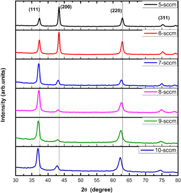
Figure 1. X-ray diffraction pattern of NiO thin films grown at different oxygen flow rates.
Download figure:
Standard image High-resolution imageAt 5 sccm of an oxygen partial pressure, G-XRD spectra of NiO phase exhibited 5 diffraction peaks located at 2θ angles of 37.33°, 43.38°, 62.84°, 75.36°, and 79.22° corresponding to (111), (200), (220), (311), and (222) cubic lattice plane, respectively. An intense preferred orientation was observed at a diffraction angle 2θ of 43.38° which corresponds to (200) orientation of cubic NiO lattice. There were no additional peaks present in the XRD spectra indicating the absence of any secondary phases. [23]. A similar diffraction pattern was observed for the films deposited at 6 sccm. At such lower oxygen partial pressures, marginally high sputtering rate is evident resulting in a high yield. A further increase in oxygen flow rate to 7 sccm reduced the (200) peak intensity moderately. The increased flow rate resulted in a marginal decrease in the film thickness due to which we have observed such decrease in peak intensity. Interestingly, we have noticed a crystallographic orientation transition from (200) to (111) plane as the oxygen content raising to sccm or higher. The increased oxygen flow rate during sputtering result in changes in the gas kinetics and the deposited molecules do not have enough mobility to settle down at a stable orientation because of the variation in the mean free path of the gas molecules. The variation in mean free path could cause the atoms to change the orientation during the growth and hence a preferred orientation along (111) was observed at higher oxygen partial pressures. Moreover, the minimization of surface energy could also be the possible reasons for such an orientation change. On the contrary, Chen et al reported that at higher oxygen flow rates, the deposited NiO thin films orientation shifted from (111) to (200) plane [24]. The sputtered NiO thin film crystallographic orientations is NaCl type of crystal structure is affected by the arrangement of Ni+2 and O−2 species [18]. At higher oxygen content, the sputtering rate gets reduced due to the greater influence of reactive oxygen atoms than the sputter gas. Therefore, sputtering yield is lower for such films because Ni atoms collide with unionized oxygen molecule left in the chamber which causes the lower sputtering rate [24].
From the G-XRD, spectra it was observed that the 2θ position of the preferred (111) orientation has slightly shifted from 37.33° to 36.86° as the oxygen partial pressure gradually increased. It might be attributed to the lattice strain present in the sputtered films. Lattice strain (ε) of the thin films was calculated by using the relation (2):

The dependence on oxygen flow rate on the crystallite size was estimated from the Debye–Scherrer equation (3):

Where λ is the wavelength of the x-rays, (Cu Kα λ = 1.54056 Å), β is the full-width at half maxima (FWHM) of the diffraction spectra and θ is the Bragg's angle to surface of the plane. The calculated crystallites size of NiO thin films is plotted with oxygen flow rate and it is shown in figure 2. Average size of crystallites 18.86 nm was obtained for the films grown at 5 sccm oxygen flow rate and the value decreased to 16.46 nm for the films grown at 6 sccm oxygen flow rate. The subsequent increase in oxygen flow rate resulted in the crystallite size of 10.19 nm, 9.80 nm, 8.45 nm, and 8.35 nm, for the films grown at 7, 8, 9 and 10 sccm, respectively. The increased oxygen content causes formation of more defects, oxygen interstitials, nickel vacancies and causes variation in grain size values [25].
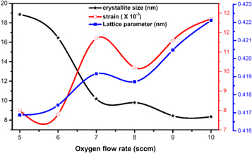
Figure 2. Variation of crystallite size, strain and lattice parameter for NiO thin films.
Download figure:
Standard image High-resolution imageStandard non-stochiometric NiO thin films lattice constant a0 is 4.1678 Å [15]. The NiO lattice parameter was calculated by using the following relation (4):

where λ is the wavelength of x-rays, h, k and l are the Miller indices, a is the lattice parameter and inter planer distance, 'd' for a cubic system are related by the following expression (5):

The extracted data for NiO thin films which include lattice parameter, grain size, dislocation density, strain, and crystallites size are summarized in a table 1. It is clearly confirming that calculated lattice parameter crucially increased from 4.1672 to 4.2211 Å and is strongly related to the increase in the oxygen content during deposition. Dislocation density was calculated by using the relation: the relation (6):

where D is the crystallite size of the film.
Table 1. The physical parameters extracted from NiO thin films.
| Oxygen flow rate (sccm) | 2θ (degree) | FWHM | Average crystallite size (nm) | Lattice strain | Lattice parameter (Å) | Dislocation density (1015m−2) | Number of crystallites (1016 m−2) |
|---|---|---|---|---|---|---|---|
| 5 | 37.33 | 0.6209 | 18.86 | 0.0080 | 4.169 | 2.81 | 3.84 |
| 6 | 37.28 | 0.5995 | 16.46 | 0.0078 | 4.174 | 3.69 | 5.35 |
| 7 | 37.12 | 0.8997 | 10.19 | 0.0117 | 4.192 | 9.63 | 24.00 |
| 8 | 37.16 | 0.7848 | 9.80 | 0.0102 | 4.187 | 10.41 | 31.87 |
| 9 | 37.00 | 0.9706 | 8.45 | 0.0127 | 4.205 | 14.00 | 38.12 |
| 10 | 36.86 | 0.9675 | 8.35 | 0.0127 | 4.221 | 14.34 | 41.22 |
3.2. Optical analysis
The optical transmittance spectra of NiO thin films grown at different oxygen flow rates extended from 5 sccm to 10 sccm is displayed in figure 3(a). As the oxygen partial pressure was raised during the deposition, we have noticed that the transmittance of the film gradually decreased particularly in the visible region.
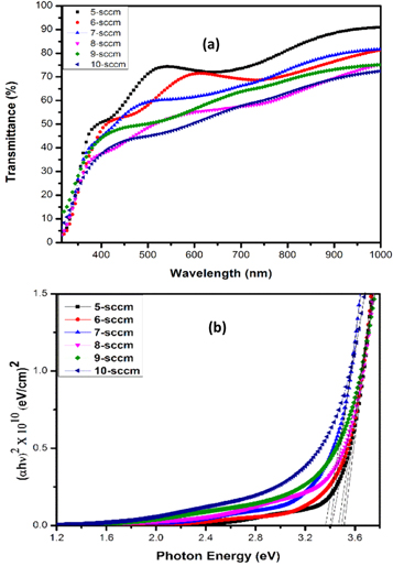
Figure 3. (a) Transmittance spectra (b) Tauc plot.
Download figure:
Standard image High-resolution imageThe measured value of transmittance of the NiO thin films was 73.46% at 5 sccm O2 flow rate. As the oxygen flow rate progressively increased to 10 sccm, film transmittance significantly decreased from 73.46% to 51% at 600 nm wavelength. At higher oxygen partial pressures lower transmittance and reduced optical band gap was observed which could be attributed to the poor crystallization formation in the films. However, transmittance of the films not only depend on the oxygen content present in the film, but grain size is also playing an important role. Excess oxygen gas atoms present in the film act as scattering centers for the incident light [26]. Hence a reduced transmittance was observed at higher oxygen flow rates. The optical properties of NiO thin films is summarized in the table 2. The computed optical band gap has decreased from 3.52 eV to 3.36 eV with increasing the oxygen flow rate from 5 sccm to 10 sccm, as shown in the figure 3(b). It is notable that the semiconductor energy band gap is shifted towards lower value and it can be influenced by the presence of strains in the films. We have observed a compressive strain in the films deposited at 5 sccm oxygen flow rate and an optical band gap of 3.52 eV was recorded. Similarly, at higher oxygen partial pressures, tensile strain affected the band gap of the films [25]. We have observed that oxygen partial pressure decides the overall optical properties of the grown films [27].
Table 2. The optical properties of NiO thin films grown at different oxygen flow rates.
| Oxygen flow rate (sccm) | Energy band gap (eV) | Transmittance (%) at 600 nm |
|---|---|---|
| 5 | 3.52 | 73.46 |
| 6 | 3.50 | 71.55 |
| 7 | 3.40 | 61.64 |
| 8 | 3.46 | 55.50 |
| 9 | 3.41 | 56.68 |
| 10 | 3.36 | 51.00 |
3.3. Chemical analysis
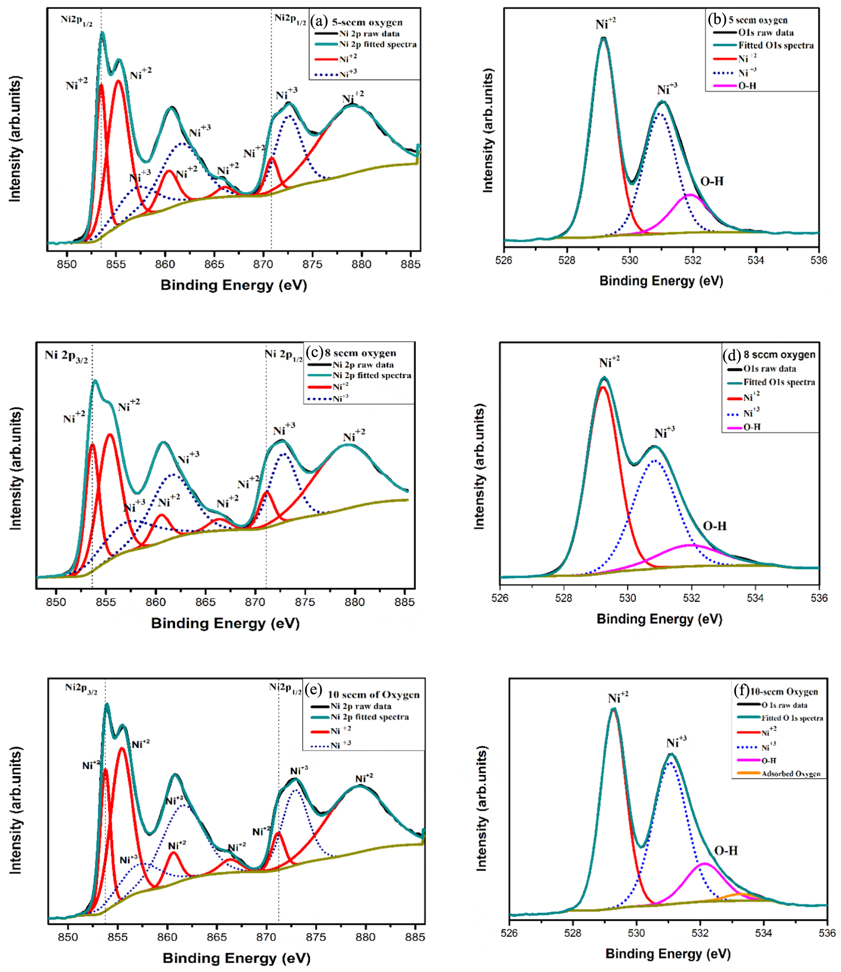
The elemental mapping was carried out from the wide survey spectra of NiO films measured over a binding energy range of 0 to 1200 eV and the graph is displayed in figure 4. The XPS spectra of the Ni 2p states of NiO thin films deposited at 50 W with varying oxygen flow rates of 5, 8, and 10 sccm are shown in figure 5.
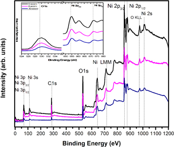
Figure 4. Wide survey XPS spectra of NiO films measured over a binding energy range of 0 to 1200 eV.
Download figure:
Standard image High-resolution image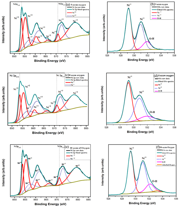
Figure 5. XPS spectra of the Ni 2p states of NiO thin films deposited with varying oxygen flow rates of 5, 8, and 10 sccm.
Download figure:
Standard image High-resolution imageAll the recorded XPS spectra were analyzed by using casa XPS software. A standard carbon peak C1s at 284.80 eV was observed in the spectra as the reference peak for all the samples and it also include Ni 2p, O 1 s peaks. In order to extract the complete information from the XPS spectrum a standard Shirley type background correction was carried out. The spectra were deconvoluted and fitted using mixed Lorentzian-Gaussian line shape (GL) to determine the NiO thin film chemical composition. The XPS survey spectrum consists of photoemission intensity peaks Ni 3p, Ni 3 s, O 1 s, Ni 2p1/2, and Ni 2p3/2 and auger electron peaks Ni LMM, O KLL;, along with adventitious carbon element (C 1 s) were also observed [28]. There are no other elemental peaks exists in the spectra clearly indicating that the deposited films does not have any foreign element in the specimen. The survey spectra of the difference between core level spectra of Ni 2 P, Ni 2p3/2 and Ni 2p1/2 are shown in the figure 5. The Ni 2p core spectra suggests a binding energy peak difference in the range 17.24 eV to 17.47 eV, which suggests that the dependence of oxygen flow rate during deposition on the chemical state [28, 29].
The Ni 2p spectra can split based on the spin–orbit coupling, Ni 2p3/2 and Ni 2p1/2 domains corresponding to binding energy in the range of 850 to 869 eV and 870 to 885 eV, respectively. The comparison between all three samples of XPS Ni 2p survey spectrum is shown in the figure 4(a), which were sputtered at different oxygen flow rates. We have not observed a marked chemical shift variation in the films sputtered at different oxygen flow rates. All three Ni 2p spectrum were individually deconvoluted using Shirley type background in the range of 850 to 885 eV of binding energy. We have observed a complex main peak, satellites structures in the spectra and based on these features we can estimate the distribution of atomic percentages, binding energy peak positions and their corresponding oxidation states. The consolidated Ni 2p spectrum values of the samples are listed in the table 3. The main line peak of the Ni 2p3/2 occur at binding energy varying from 853.58 to 853.72 eV with their corresponding full width half maxima (FWHM) value between 1.24 to 1.59 eV [30]. Broadening of the main peak and their satellites structures depend on the oxygen deficiency and/or interaction of Ni atom with their neighboring NiO6 octahedra [31]. Based on the interpretation of Ni 2p spectra, satellites and number of shake up peaks are originated in higher level of binding energy of the Ni 2p3/2 and Ni 2p1/2 region due to mixing of d-d transition and enhancement of Ni3d—O2p hybridization [30, 32].
Table 3. The XPS Ni2p and O1s spectral peak positions and atomic percentages of the NiO thin films.
| O2 flow rate | Ni 2p Ni2+ | FWHM | Atomic % | Ni 2p Ni3+ | FWHM | Atomic % | O 1 s | O 1s FWHM | Atomic % |
|---|---|---|---|---|---|---|---|---|---|
| 5 sccm | 853.58 | 1.24 | 10.14 | 857.22 | 5.00 | 7.84 | 529.16 | 0.97 | 49.15 |
| 855.25 | 2.52 | 19.49 | 861.51 | 5.00 | 15.98 | 530.95 | 1.41 | 36.84 | |
| 860.35 | 2.20 | 4.39 | 872.53 | 3.13 | 12.05 | 531.91 | 1.21 | 14.01 | |
| 866.04 | 2.01 | 1.05 | |||||||
| 870.82 | 1.45 | 2.77 | |||||||
| 878.75 | 7.37 | 26.34 | |||||||
| 8 sccm | 853.62 | 1.59 | 10.82 | 857.23 | 6.52 | 10.38 | 529.22 | 1.19 | 49.86 |
| 855.32 | 2.69 | 18.09 | 861.52 | 5.00 | 17.00 | 530.83 | 1.61 | 38.94 | |
| 860.47 | 2.08 | 3.08 | 872.75 | 3.17 | 11.58 | 531.91 | 2.38 | 11.20 | |
| 866.33 | 2.60 | 1.62 | |||||||
| 871.09 | 1.73 | 3.25 | |||||||
| 878.93 | 7.13 | 24.17 | |||||||
| 10 sccm | 853.72 | 1.18 | 8.83 | 857.21 | 5.06 | 7.49 | 529.27 | 0.93 | 43.85 |
| 855.35 | 2.57 | 20.51 | 861.50 | 5.00 | 19.61 | 531.00 | 1.26 | 41.96 | |
| 860.56 | 1.76 | 2.89 | 872.86 | 3.08 | 12.01 | 532.10 | 1.39 | 12.41 | |
| 866.33 | 2.48 | 1.73 | 533.26 | 1.11 | 1.78 | ||||
| 871.15 | 1.52 | 2.93 | |||||||
| 879.02 | 7.00 | 24.02 |
The Ni 2p binding energy peaks of the XPS spectra were analyzed by various researchers. Sasi et al reported binding energy peaks at 856.5, 862, 873.7 and 880 eV correspond to Ni2O3 phase for the as deposited thin films. In addition, they have also assigned the peaks at 857.1, 863 eV to the Ni+3 state [33, 34]. Similarly, Dong-soo kim et al, deconvoluted XPS Ni 2p spectra and distinguished the oxidation states based on their binding energy peaks. The obtained peaks at 854.5, 856, 861.5, 873 and 879.8 eV indicated Ni+2 states and the peaks at 856.1, 861.7 eV were assigned to Ni+3 state [35]. Jung Kyu Kim reported multiple peaks in Ni2p core spectra binding energies of 854.1, 872.0 corresponding to Ni+2 state. The peaks at 856.1 and 873.9 eV were assigned to Ni+3 states [36]. These trends are strongly in agreement with our XPS results and obtained multiple peaks are successfully assigned to Ni+2 and Ni+3 states with their total area of the peak summarized in table 3.
Figures 5(b), (d) and (f) shows the O1s spectrum deconvoluted into 3 peaks by using Shirley type background and fitted with the Lorentzian-Gaussian (GL) line shape. The characteristic core level O1s peak located at ~529.16 to 529.27 eV is ascribed to Ni+2 because of lattice oxygen interaction in the form of Ni–O octahedral bonding of NiO [37]. The peak at 530.83 to 531 eV represent the Ni+3 which indicate vacancy or metal deficiency in the films and a small peak located at ∼531.90 to 532.10 eV represents the O–H group and 533.26 eV represents the adsorbed O2 element present in the deposited NiO surface layer [11, 38]. The oxidation state of Ni+2 peak position is slightly shifted from 529.16 to 529.27 eV with increase in the oxygen partial pressure from 5 to 10 sccm during the deposition. The lattice oxygen atomic percentages notably decrease from 49.15% to 43.85% with increasing oxygen content to 10 sccm. It clearly tells us that deposited film at lower oxygen flow rate removes the oxygen defects and enhance the Ni-O lattice. Similarly, the surface area of the Nickel vacancy state (Ni+3) is increased from 36.84% to 41.96% as increasing oxygen rate from 5 to 10 sccm. Therefore, we conclude that at higher oxygen flow rate, grown NiO thin films create more nickel vacancies and oxygen interstitials and are mainly responsible for p type conductivity. We have also used the XPS data to find the difference in the atomic percentages of the metal and oxygen ions. And it was observed that there was only a marginal difference in the  ratio . We have obtained the ratio of
 ![$\left[\tfrac{Ni}{O}\right]$](https://content.cld.iop.org/journals/2053-1591/7/1/016427/revision2/mrxab69c5ieqn2.gif) as 1.162, 1.26, and 1.165 at oxygen partial pressure of 5, 8 and 10 sccm, respectively, which implies the excess Ni composition in the films. In addition, from the deconvoluted NiO XPS spectra, the calculated ratio of
as 1.162, 1.26, and 1.165 at oxygen partial pressure of 5, 8 and 10 sccm, respectively, which implies the excess Ni composition in the films. In addition, from the deconvoluted NiO XPS spectra, the calculated ratio of  slightly increased from 0.55 to 0.64 as a function of increased oxygen oxygen flow rate. Therefore, it is concluded that, for the deposited film at higher oxygen content, more number of Ni+2 ions are getting ionized and converted into Ni+3.
We have also noticed that there is a small chemical shift in the main peaks and their satellites of Ni2p and O1s spectra when we deposited films at higher oxygen flow rates. We have also observed O1s chemical shift which is normally reflected in the Ni2p spectra. This kind of shift in binding energies are attributed to charging effect, i.e., changes in the ionic charge broadening of the peaks and creating cation vacancies by induced oxygen [39, 40].
The resistivity of the sputtered NiO thin films decrease because of the formation of defects structure due to vacant positions of Ni+2 ions occupied by Ni+3 cations, when introducing more oxygen content during the deposition. The origin of defects in films due to the loss of oxygen, influences local coordination number in defective NiO [32]. However, with increase in the oxygen flow rate, change in stoichiometry is shown in the table 3. According to Kroger-Vink notation, the origin of Ni vacancy due to neighboring two Ni+2 will ionize into Ni+3 by donating one extra electron to oxygen and it could be represented by following equation (7):
where 


 stands for Ni+2, Ni+3, the ionized Nickel vacancy and O−2 ions respectively. Generally, the formation of ionized Ni vacancies and Ni+3 ions located the top of the valence band served as an acceptor. It is mainly accountable for the p-type conductivity of NiO thin films [35, 41].
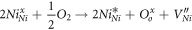
The sputtered NiO thin films exhibited mainly five peaks in the Raman spectra as shown in figure 6. The following Raman bands were observed for all the films; the first order transverse mode (TO) at 458 cm−1 and first order longitudinal (LO) mode shifted from 554.18 cm−1.The bands at 945.50 cm−1 to 951.98 cm−1 were assigned to the combination of TO + LO phonon excitation mode of NiO thin films. The stronger second order bands located at 783.46 cm−1 represents a transverse (2TO) mode and another band located at 1093.20 cm−1 represents the longitudinal (2LO) mode in the NiO film. The shifting of their band position leads to the small variations observed in the crystallinity of the sputtered NiO thin films. First order LO mode and second order 2LO modes are associated with the vibration of Ni—O bonds and also the sharp intense band around 554.18 to 560.37 cm−1 indicates the existence of Nickel defects or Ni+3 ions exist along with the Ni+2 ions which were also confirmed by the XPS characterization [11].
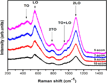
Figure 6. Raman spectra of NiO thin films.
Download figure:
Standard image High-resolution image3.4. Surface analysis
Figure 7 depicts AFM images of the NiO thin films performed in tapping mode with scan area ~2 μm × 2 μm. The images reveal a smooth surface morphology and deposited NiO particles are distributed uniformly over the entire scan region. The root-mean-square (rms) roughness of the NiO films grown at 5 sccm oxygen flow rate was 5.10 nm. There was a marginal increase in the surface roughness for the films deposited at 6 sccm and the measured roughness was 6.17 nm. Progressive increase in the oxygen flow rate towards 10 sccm lead to the further reduction in the surface roughness of the film. A similar trend was also observed for the average particle height as depicted in the table 4. These results are in accordance with the behavior of crystallization of grown thin films as observed from the computed grain sizes through XRD spectra. The sputtering rate marginally decrease as the oxygen flow rate during deposition increase and eventually sputtered films become smoother.
Figure 7. Atomic force microscopy images of NiO thin films grown at different oxygen flow rates.
Download figure:
Standard image High-resolution imageTable 4. Surface roughness and average particle height of NiO thin films.
| Oxygen flow rate (sccm) | Particle height (nm) | Roughness (Rq) |
|---|---|---|
| 5 | 7.12 | 5.10 |
| 6 | 13.97 | 6.17 |
| 7 | 7.99 | 3.10 |
| 8 | 4.09 | 2.22 |
| 9 | 4.85 | 2.02 |
| 10 | 5.10 | 1.95 |
3.5. Electrical properties
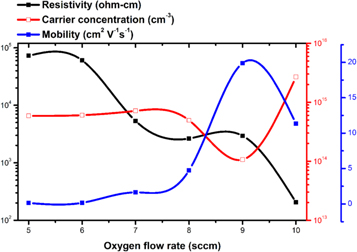
The electrical studies of sputtered NiO thin films were performed by using Hall measurements tool under a magnetic field of 0.60 T at room temperature. The parameters such as resistivity, carrier concentration, carrier type, and Hall mobility were extracted from the measurement. Figure 8 represents the dependence of oxygen flow rate (sccm) on the electrical properties of the deposited NiO thin films at room temperature. An increase in the oxygen flow rate from 5 to 10 sccm resulted in a sharp decrease in the electrical resistivity of the films. It can be seen that the resistivity of the film for 5 sccm of oxygen flow rate is 7.3 × 10⁴ Ω-cm and as increasing the oxygen up to 10 sccm during the sputtering resulted in a resistivity ∼1.4 × 10² Ω-cm. The XPS spectra confirms that the higher oxygen flow rate results in increased Ni+3 ions, leading to the formation of Ni vacancies in the NiO film which promotes the reduced resistivity. An order of magnitude variation (∼1014 to 1015 cm−3) in the carrier concentration was also observed because of the increment of an oxygen content during the sputtering process. Consequently moreover, the carrier mobility of the films also varied from 0.453 to 20.60 cm2 V-1s−1 as function of oxygen partial pressure.
Figure 8. Electrical properties of NiO thin films grown at different oxygen flow rates.
Download figure:
Standard image High-resolution image
Interestingly, n-type conductivity was observed that the NiO film deposited at 5 and 6 sccm oxygen content. A stable p-type electrical conductivity was also observed for the films grown at higher oxygen partial pressures of 7 to 10 sccm. In other words, we were able to grow both p- and n-type NiO thin films depending on the oxygen flow rate during deposition. The conversion of conductivity type could be attributed to the changes in the crystalline structure and defect states as explained in the previous sections.
In general, the n-type behavior of NiO film arises from the oxygen vacancies and the p- type behavior arises from the nickel vacancies. Table 5 display the electrical parameters obtained from the Hall effect measurement for the sputtered NiO thin films grown at various O2 flow rates. An increased oxygen content during the sputtering process resulted in the drastic reduction in the electrical resistivity which is believed to be due to decreased oxygen vacancies and free electrons. Besides, the carrier mobility continuously enhanced to 19.89 cm2 V-1s−1 with increased oxygen flow rate, and subsequently the mobility values reduced to 11.33 cm2 V-1s−1 with further increase in flow rate to 9 sccm. The decreased mobility is owing colloidal energy loss of the particles with oxygen during sputtering process [42]. The tunable electrical properties of NiO thin films with oxygen flow rate could be associated with the point defects, microstructure and composition [43]. In addition, variation of electrical properties of the films not only rely on oxygen partial pressure, but other deposition parameters such as sputter power, target surface, sputter pressure also plays crucial role. Hence, by controlling these parameters possible to produce the desired film properties [44].
Table 5. Various electrical properties of NiO thin films.
| Oxygen flow rate (sccm) | Resistivity (Ω-cm) | Carrier concentration (cm−3) | Mobility (cm2 V−1 s−1) | Carrier type |
|---|---|---|---|---|
| 5 | 7.3 × 10⁴ | 5.9 × 10¹⁴ | 0.15 | n |
| 6 | 6.1 × 10⁴ | 6.0 × 10¹⁴ | 0.17 | n |
| 7 | 5.3 × 10³ | 7.1 × 10¹⁴ | 1.64 | p |
| 8 | 2.6 × 10³ | 4.9 × 10¹⁴ | 4.74 | p |
| 9 | 2.9 × 10³ | 1.1 × 10¹⁴ | 19.9 | p |
| 10 | 2.0 × 10² | 2.7 × 10¹⁵ | 11.3 | p |
4. Conclusions
In summary, we have investigated the dependence of oxygen flow rate on sputtered NiO thin films by reactive dc magnetron sputtering. XRD data reveal that crystallographic orientation strongly depend on the oxygen content present during the deposition of the NiO thin films. Optical measurements suggest a significantly reduction in the transmittance from 73.46 to 51% at 600 nm region and calculated energy band gap value varied from 3.52 eV to 3.36 eV with increased oxygen flow rate. The XRD results demonstrate a polycrystalline nature with FCC phase. The preferred orientation changing from (200) to (111) suggest the presence of both compressive and tensile strain in the films. The reduction in the surface roughness of the films with an increase in oxygen partial pressure was observed through AFM analysis. The Raman band shifts attributed to the changes in the crystallinity in the films. Deconvolution of XPS spectra revealed that atomic percentages have varied systematically with variation in the oxygen flow rate. The increased oxygen atoms during sputtering results in the formation of Ni+3 ions. The defects states confirm the presence of Ni+2 and Ni+3 in the film, which cause the reduced resistivity of the films from 104 to 102 Ω-cm. It was also found that the conductivity of grown NiO thin films tuned from n-type to p-type as the oxygen flow rate increased during deposition.
Acknowledgments
The authors are thankful to Manipal Academy of Higher education for financial support under the T M A Pai PhD Scholarship programme. A part of this research work was using facilities at CeNSE, funded by the Ministry of Electronics and Information Technology (MeitY), Government of India, and located at the Indian Institute of Science, Bengaluru.
Conflicts of interest
There are no conflicts of interest to declare.