

Abstract
To study the capability of the CdSe thin films to use as an absorber layer in semi-transparent thin film solar cells, the structural, optical, electrical and photovoltaic properties of thermally evaporated CdSe thin films (thickness 300 nm) as a function of silver-doping were investigated. A novel and facile method was used to Ag-doping of the samples. Some aqueous solution of silver nitrate (with various concentration) was spin coated onto the surface of CdSe thin films followed by air-annealing to diffuse silver dopants into the layers. The field emission scanning electron microscope (FE-SEM) images showed that the surface of CdSe thin films was improved with our doping method. X-ray diffraction (XRD) analysis revealed the hexagonal structure of the samples. The crystallite size, micro-strain and dislocation density of CdSe thin films were evaluated using XRD patterns. The transmittance spectra in the wavelength range of 400–2500 nm were measured and then used to study other optical parameters. The optical energy band gap was decreased with Ag-doping from 1.96 eV to 1.67 eV. The electrical conductivity of FTO/CdSe:Ag/Al Schottky junction devices was improved by Ag-doping, and the photovoltaic efficiency was increased by Ag-doping form 1.53% for the undoped sample to 2.78% for the sample with the highest doping concentration. Obtained results show that Ag-doped CdSe thin films are a promising candidate to use as an absorber layer in semi-transparent solar cells and colorful photovoltaic windows.
Export citation and abstract BibTeX RIS
1. Introduction
Semi-transparent solar cells are a kind of photovoltaic cell in which the thickness of the absorber layer is low enough to provide the desired amount of transparency. These solar cells are used as photovoltaic windows in green buildings. Dye-sensitized solar cells (DSSC) are commonly used as photovoltaic windows. Also, a-Si, CdTe and CIGS thin films are used as an absorber layer in semi-transparent thin film solar cells [1–4], but there is no report about the usage of CdSe thin films as an absorber layer in semi-transparent solar cells. Cadmium Selenide (CdSe) is an n-type, reddish semiconductor material. CdSe thin films have been used in photovoltaic devices because of their suitable direct band gap (about 1.74 eV for bulk CdSe material), high absorption coefficient and electrical conductivity [5, 6]. There are many reports about the usage of the CdSe thin films as a window layer in the CdTe based thin film solar cells. Li et al studied the effect of substrate temperature on the performance of the CdSe(window layer)/CdTe thin film solar cell [7]. Bao et al reported the usage of oxygenated CdSe thin films as a window layer in the CdTe based thin film solar cells [8]. Moreover, there are many reports about CdSe QD sensitized solar cells [9, 10]. Schottky junction solar cells are a type of solar cell in which the charge separation is performed by the Schottky barrier between the absorber layer and the electrode. There are some reports about the CdSe based Schottky barrier solar cells. Gao et al [11] studied the performance of graphene/CdSe nanobelt/Au Schottky barrier solar cells. They used graphene as a transparent electrode and the Schottky barrier was formed at the graphene/CdSe nanobelt interface. The performance of graphene/CdSe nanobelt/Ag Schottky junction solar cell was reported by Zhang et al [12]. Kumar et al [13] and Manna et al [14] studied the electrical properties of Al/CdSe thin film contacts and reported the formation of the Schottky barrier at Al/CdSe interfaces. The aim of the present work is to investigate the capability of CdSe thin films to use as an absorber layer in the semi-transparent Schottky junction thin film solar cells. The thickness of the CdSe thin film was chosen as 300 nm to achieve the required transparency. In this work, we have chosen thermal evaporation technique to fabricate CdSe thin films because it can be used to prepare homogeneous thin films with controlled thickness. CdSe thin films evaporated into the FTO substrates to form ohmic contact and Schottky junction was formed by evaporating aluminum onto the CdSe thin films by using an appropriate mask. The efficiency of the solar cells is related to the physical properties of the absorber layer which can be altered by thermal annealing and metal-doping [15, 16]. Zhao et al [17] studied the effect of Ag-doping on the electronic and optical properties of CdSe quantum dots by using density functional theory. They reported that silver-doping increases the number of charge carriers and enhances the performance of CdSe QDs for their potential applications in high-efficiency photovoltaic devices. Lee et al [18] reported that Ag-doped CdSe SQDs exhibit n-type doping behavior which implies the enhancement of charge carriers. Tung et al [19] studied the effect of Ag-doping on solar cell efficiency of the CdSe QDs sensitized solar cell. They reported that the performance of the cells was improved from 0.82% to 2.72% as the result of Ag-doping. According to the literature, it can be suggested that Ag-doping can alter the performance of CdSe based thin film solar cells. In the present work, we have studied the effect of Ag-doping on the performance of FTO/CdSe/Al semi-transparent Schottky junction solar cells. There are few reports on the Ag-doped CdSe thin films. Kaur and Triphathi [20] studied the properties of annealed and light-soaked Ag-doped CdSe thin films. Also, Kaur et al [21] reported that the optical and electrical properties of CdSe thin films alter with Ag-doping. In these works, doped CdSe material was synthesized with melt quenching technique, and samples were fabricated by thermal evaporation method. In present work, we have used a novel, facile and inexpensive method to fabricate Ag-doped samples. At first, some silver nitrate aqueous solution (with various concentration to achieve the various amounts of silver-doping) coated onto the surface of CdSe thin films by spin coating technique. Then, these samples were air-annealed to diffuse silver dopants into the layers. Furthermore, the structural, optical, electrical properties of the CdSe thin film were studied as a function of doping concentration, because the performance of samples is related to the physical properties of CdSe thin films. The results showed that CdSe thin films are a promising candidate to utilize as an absorber layer in semi-transparent Schottky junction thin film solar cells and Ag-doping is an effective method to improve the performance of these devices.
2. Experimental
The CdSe thin films were deposited onto glass and FTO coated glass substrates using an Edwards 306 A coating system. The CdSe powder (Aldrich, 99.99%) was used as source material. At first, substrates were cleaned with subsequent sonication in detergent, ethanol, acetone and deionized water, and then blow dry with nitrogen. Thin film deposition was carried out at a vacuum of 4 × 10⁻⁶ mbar and at room temperature. The thickness of thin films and the deposition rate were monitored by using a quartz crystal system. The deposition rate was about 0.5 Å/s, and the thickness of samples was about 300 nm. After deposition, the samples were air-annealed at the temperatures of 300 °C for 90 min. It must be mentioned that the undoped sample in this paper is a sample that once air-annealed at 300 °C for 90 min. Then, some samples were silver-doped via spin coating (2500 rpm, 15 s) of silver nitrate solution in deionized water (0.002, 0.004, 0.006 and 0.008 M which will be called, S1, S2, S3 and S4, respectively in this paper) onto the surface of samples. Furthermore, these samples were air-annealed again at 300 °C for 90 min to diffuse dopants into the CdSe thin films. Undoped and Ag-doped CdSe thin films which deposited onto the glass substrates were used to study the structural and optical properties. Undoped and Ag-doped CdSe thin films which deposited onto the FTO coated glass substrates were used to fabricate Schottky junction solar cells (FTO/CdSe/Al and FTO/CdSe:Ag/Al devices) to investigate the electrical and photovoltaic properties. At the end of the fabrication process, aluminum as the top electrode was evaporated onto FTO/CdSe samples using an appropriate mask. The effective area of the top electrode is 9 mm2. It is worthwhile to mention that, the transparency of CdSe thin films was reduced by increasing the doping concentration higher than 0.008 M and it was not suitable to use as an absorber layer in semi-transparent solar cells, so we did not study higher doping concentration in the present work. The surface morphology of the CdSe thin films was investigated using field emission scanning electron microscopy (FE-SEM; MIRA3 TESCAN). The elemental composition of the Ag-doped specimens was studied by EDX analysis (MIRA3 TESCAN). The structural properties of undoped and Ag-doped CdSe thin films were studied by using an x-ray diffractometer (Cu Kα, Explorer-GNR). The optical transmittance of thin films was measured in the wavelength range of 400–2500 nm by using Perkin Elmer lambda-9 UV/Vis/NIR spectrophotometer. The photovoltaic characterization was carried out under AM 1.5 illumination by using SIM-1030 (Sharif Solar, solar simulator) and a homemade I-V meter.
3. Results and discussions
3.1. Surface morphological and structural properties
The surface morphology of undoped and Ag-doped CdSe thin films was investigated using FE-SEM images, as shown in figure 1. As can be seen, figure 1(a), the surface of the undoped sample is cracked that caused as the result of thermal annealing. (The surface of pristine deposited CdSe thin films is homogeneous, as shown in Supplementary file). It can be due to the difference in thermal expansion coefficients between CdSe thin film and substrate [22]. Such behavior was reported by Punitha et al [23] and Chandar et al [24] for annealed CdTe thin films. As can be observed in figure 1, the surface of Ag-doped samples is cracked too, but the surface of these samples is less cracked than the undoped sample. It can be caused by the Ag-doping process. Silver dopants that penetrate into the cracks bond with the atoms of the crack's walls. These bonds, like an adhesive, bond the atoms of the two sides of the crack's walls together. As mentioned in the experimental part, samples were air-annealed at 300 °C for 90 min after the spin coating of silver nitrate solution. Thermal annealing provides the required energy to break weaker bonds between the atoms of the CdSe layer [25], so these atoms will be moved together by the driving force caused by the mentioned bonds between silver dopants and these atoms. This can lead to nucleation and growth of the CdSe crystallites in the cracks and fill them. This phenomenon can be responsible for reducing the surface cracks of the doped samples compared to undoped ones.
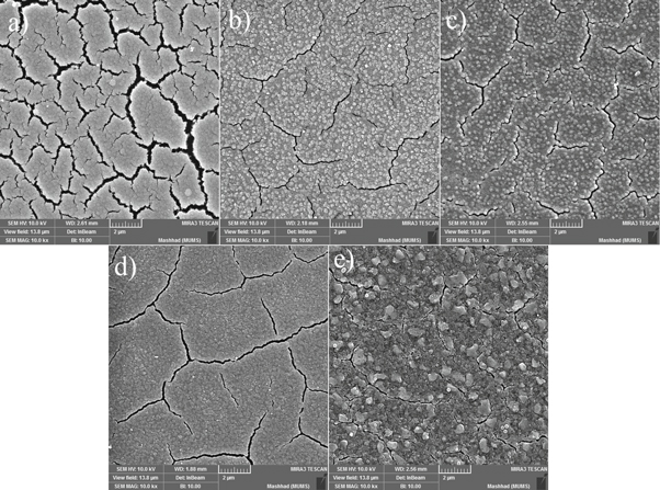
Figure 1. FE-SEM images of the undoped CdSe thin film (a),  (b),
(b),  (c),
(c),  (d) and
  (e) samples.
Download figure:
Standard image High-resolution imageXRD patterns of the undoped and Ag-doped CdSe thin films are shown in figure 2. The observed diffraction peaks are in agreement with the standard data (JCPDS File no. 08-0459) and CdSe thin films have hexagonal (würtzite) structure. No peaks related to Ag or Ag2Se are observed in diffraction patterns. The preferred orientation of all samples is along (002) plane. The crystallinity of the S1 sample is improved sharply compared to the undoped sample. It can be attributed to the enhancement of the surface quality and decrease of surface cracks after silver-doping. Also, the crystallinity is decreased by increasing the doping concentration. It can be due to the entrance of silver dopants as localized defects into the CdSe layer.
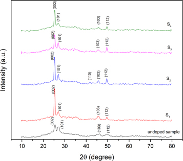
Figure 2. X-ray diffraction patterns of the undoped and Ag-doped CdSe thin films.
Download figure:
Standard image High-resolution imageThe lattice constants of hexagonal structure (a) and (c) were calculated using the following equation [26] and tabulated in table 1.

where a and c are the lattice constants, h, k and l are Miller indices and dhkl is the interplanar crystal spacing that can be calculated using Bragg's formula.
Table 1. Calculated and standard lattice parameters of undoped and Ag-doped CdSe thin films.
| Lattice parameter (a) (Å) | Lattice parameter (c) (Å) | |||
|---|---|---|---|---|
| Sample | Calculated standard | Calculated standard | ||
| Undoped | 4.3413 | 4.2990 | 6.9359 | 7.01 |

|
4.3052 | 7.0522 | ||

|
4.3120 | 7.0237 | ||

|
4.3087 | 7.0503 | ||

|
4.3084 | 7.0244 | ||
As can be seen in table 1, there is a difference between calculated and standard lattice parameters. It can be interpreted that samples are under strain due to the deposition, annealing and Ag-doping. The micro-strain and average crystallite size of the thin films can be calculated using Williamson-Hall equation [27],

where β is the full width at half maximum (FWHM) of diffraction peaks, λ is the wavelength of x-ray, θ is the Bragg angle and ε is the micro-strain. The values of micro-strain and average crystallite size were evaluated from the slope and intercept of βCosθ versus Sinθ plots, as shown in figure 3. The obtained results are listed in table 2.
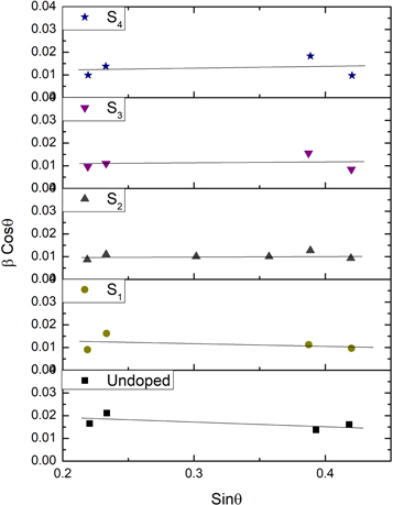
Figure 3. Variation of βCosθ with Sinθ for the undoped and Ag-doped CdSe thin films.
Download figure:
Standard image High-resolution imageTable 2. Structural parameters of undoped and Ag-doped CdSe thin films.
| Sample | D (nm) | ε × 10−4 |

|
|---|---|---|---|
| Undoped | 6 | −50 | 2.78 |

|
9.2 | −28 | 1.18 |

|
13.3 | −1.5 | 0.56 |

|
14.7 | 14 | 0.46 |

|
13.5 | 21 | 0.55 |
The negative slope means that specimens are under the compressive strain and the positive slope indicates the presence of tensile strain in the samples [28]. It is found that three specimens, S1, S2 and undoped samples are under compressive strain. The value of the mentioned micro-strain decreases with silver-doping and increasing the doping concentration. It can be due to the larger radius of dopant atoms which leads to the expansion of the crystal lattice. The type of micro-strain is changed to tensile strain with increasing the doping concentration for S3 and S4 specimens and its value increased with increasing the doping concentration. The entrance of dopant atoms into the crystal lattice decreases the crystallinity of the samples and increases the value of micro-strain. As can be seen, the crystallite size increases with Ag-doping and increasing the doping concentration that can be due to the difference between the ionic radius of Ag+ (0.115 nm) and host Cd2+ (0.097 nm) ions. The entrance of larger silver ions into the crystallites makes them increase their size. Also, decreasing of crystallite size with doping was reported for Sb [29] and Zn-doped CdSe thin films [30] that have smaller ionic radius dopants. As can be observed, the value of crystallite size decreases for sample S4 compared to sample S3. Such behavior was reported for Ag-doped ZnO thin films in which the average crystallite size increases with silver-doping and then decreases for larger doped samples [31]. It can be attributed to the incorporation of dopant atoms in the grain boundary of crystallites that act to pin grain boundaries and therefore limit grain boundary mobility which leads to the reduction of the crystallite grain size [31–33]. The micro-strain increases with Ag-doping and increasing the doping concentration, that can be due to the entrance of Ag atoms in the CdSe structure. Furthermore, the dislocation density ( ) of the thin films was calculated using the following equation [34] and tabulated in table 2.

The dislocation density is an imperfection in the crystal structure. It is observed that the value of δ decreases with silver-doping and increasing the doping concentration. This parameter is related to the average crystallite size because the crystallite boundaries as an imperfection in the crystal structure are decreased by increasing the average crystallite size.
Moreover, to prove the existence of silver in the doped CdSe thin films, energy dispersive x-ray analysis (EDX) was used. Figure 4 shows the EDX patterns of doped specimens deposited onto glass substrates. The tables of relative elemental composition confirm that these samples consist of cadmium, selenium and silver. The peaks of oxygen and silicon in EDX patterns are corresponding to the glass substrates. Also, the peaks of gold in EDX patterns are corresponding to the ultra-thin gold layer which coated onto the surface of samples for FE-SEM analysis.
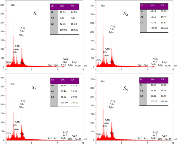
Figure 4. Energy dispersive x-ray analysis patterns of the Ag-doped CdSe thin films.
Download figure:
Standard image High-resolution image3.2. Optical properties
To investigate the optical properties of undoped and Ag-doped CdSe thin films, the transmittance spectra were measured in the wavelength range of 400–2500 nm and shown in figure 5. All samples are highly transparent in the near-infrared region, and the transmission decreases rapidly with decreasing the wavelength at the visible region. The energy of photons in the near-infrared region is lower than forbidden band gap energy and can't excite electrons from the valence band to the conduction band of CdSe thin films. It means the low absorption of energy in this region. The energy of photons in the visible region is higher than NIR region that can be absorbed by excited electrons as well as other trap levels which may exist in the band gap. The transmission decreases with increasing doping concentration which implies that silver dopants incorporated into the trap levels in the forbidden band gap [35].
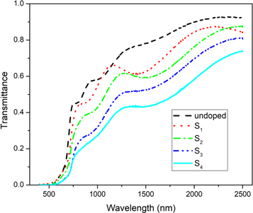
Figure 5. Variation of the transmittance with the wavelength for the undoped and Ag-doped CdSe thin films.
Download figure:
Standard image High-resolution imageTo find more, the absorption coefficient, α, of the samples was investigated by using following relation [23],

where d is the thickness of thin films and T is the transmittance. The variation of α with photon energy is shown in figure 6. As can be seen, the absorption coefficient increases with increasing doping concentration. This indicates that diffused silver dopants act as trap centers and increase the absorption coefficient which can be proved by studying the Urbach energy of samples. Also, another absorption mechanism can be proposed for the Ag-doped samples. Silver acts as an n-type dopant for CdSe thin films [19], it means that the charge carrier concentration in conduction band increases with silver-doping. These extra electrons can incorporate in the absorption of incident photon's energy via electron-photon interaction and consequently increase the absorption coefficient. All samples have high absorption in visible region that introduce them as a promising candidate for use as an absorber layer in the thin film solar cells.
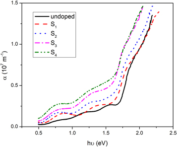
Figure 6. Variation of the absorption coefficient with the photon energy for the undoped and Ag-doped CdSe thin films.
Download figure:
Standard image High-resolution imageTo study the tailing of the density of states into the normally forbidden energy, the Urbach energy, the following equation [36] was used,

where α is the absorption coefficient, α0 is a constant and Eu is the width of the Urbach tail (Urbach energy). As can be seen in figure7, the variation of Ln(α) with hν is linear near the absorption edge, and Urbach energy can be evaluated from the slope of this region. From table 3, the Urbach energy of CdSe thin films increases with Ag-doping and increasing doping concentration. Silver dopants which added to the CdSe crystal structure act as localized states in the forbidden band gap. these localized states are a kind of traps and increasing the doping concentration means to increase the trap levels in the forbidden band gap.
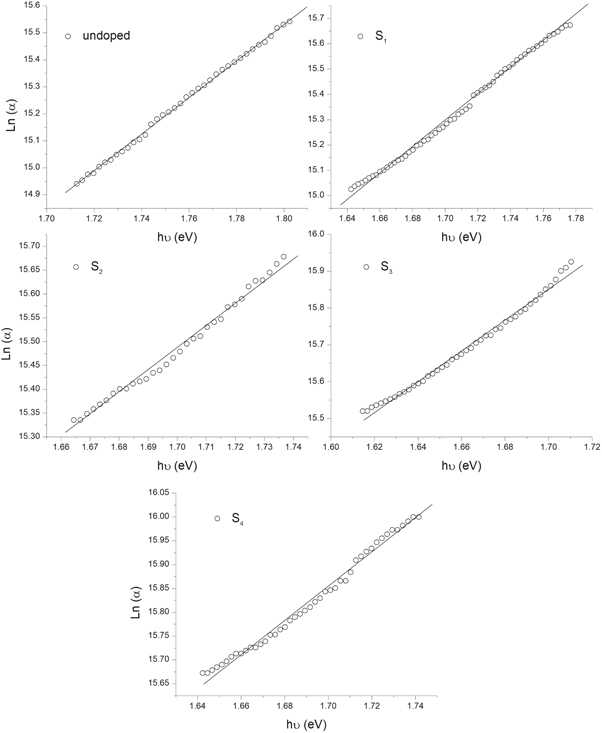
Figure 7. Plots of the Ln(α) versus hν for the undoped and Ag-doped CdSe thin films.
Download figure:
Standard image High-resolution imageTable 3. Variation of the optical energy band gap and Urbach energy of CdSe thin films with respect to Ag-doping.
| Sample |
 (eV) (eV) |
 (meV) (meV) |
|---|---|---|
| Undoped | 1.96 | 150 |

|
1.9 | 191 |

|
1.89 | 240 |

|
1.79 | 258 |

|
1.67 | 291 |
According to the transmittance spectra of the undoped and silver-doped samples, there is a red shift in the absorption edge of the specimens The optical energy band gap of the undoped and Ag-doped thin films was evaluated by using the following equation [37]:

where Eg is the optical energy band gap and B is a constant. Figure 8 shows the variation of (αhυ)2 as a function of hυ for undoped and Ag-doped CdSe thin films. The value of Eg was evaluated via extrapolating the linear region of (αhυ)2 versus hυ plots to (αhυ)2 = 0, shown in figure 8, and tabulated in table 3. It is observed that the optical energy band gap decreases with Ag-doping and increasing doping concentration from 1.96 eV to 1.79 eV. The decrement of the optical band gap is in agreement with the extension of localized states in the band gap, because increasing the tailing of trap levels in the forbidden band gap decreases the width of this region [20, 38]. Also, it can be due to the enhancement in the lattice disorder by the entrance of dopant atoms into the host crystal structure [39]. The decrease of the optical energy band gap indicates that Ag-doping can improve the performance of the CdSe based thin film solar cells.
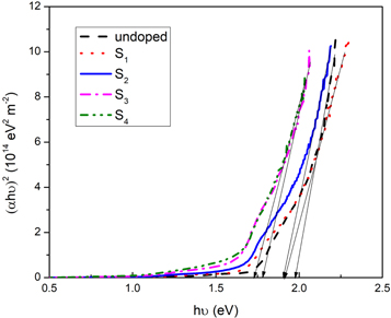
Figure 8. Plot of the (αhν)2 versus hν for the undoped and Ag-doped CdSe thin films.
Download figure:
Standard image High-resolution image3.3. Electrical and photovoltaic properties
The current-voltage characteristic of FTO/CdSe:Ag/Al devices in the dark condition is shown in figure 9. As can be seen, the conductivity of the samples is increased by increasing doping concentration that can be due to the enhancement of charge carrier concentration as the result of Ag-doping [19]. Such behavior is reported by Sharma et al [40] for CdSe:Ag thin films fabricated by using the chemical bath deposition technique. Also, it can be attributed to the change of the crystallinity of samples, reduction of compressive micro-strain and dislocation density, increasing the crystallite size and decrement of barrier height between the electrode and CdSe thin films [41, 42]. The increase of conductivity indicates that Ag-doping can improve the performance of CdSe thin films in the solar cell structure. The observed rectification behavior in I-V curves implies that Schottky contact formed between the CdSe thin film and aluminum electrode (CdSe/Al) [43]. The formation of CdSe/Al Schottky contact was reported by other researchers [14, 44, 45]. It is suggested that the thermionic emission may be the dominant conduction mechanism under forward bias, (FTO wired positive).
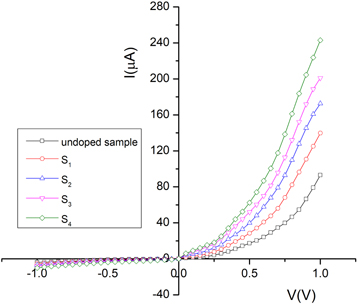
Figure 9. I-V characteristic curves of the FTO/CdSe/Al devices in dark condition.
Download figure:
Standard image High-resolution imageThe relation between current and applied voltage in this theory is given by [46]:

where n is the diode ideality factor, k is the Boltzmann constant and I0 is the saturation current which can be expressed as:

where A is the effective area, A* is Richardson constant and Φb is the barrier height between CdSe thin films and aluminum electrode. The values of n were evaluated from the linear region of the Ln (I) versus V plots, figure 10, and tabulated in table 4. Also, the value of barrier height was calculated by using the following equation:

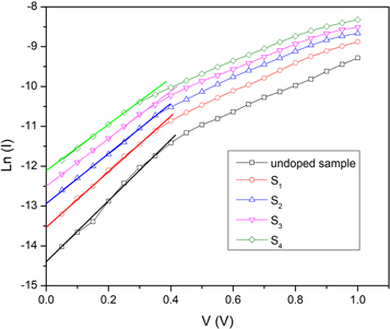
Figure 10. Semi-log forward bias I-V curves of the FTO/CdSe/Al devices in dark condition.
Download figure:
Standard image High-resolution imageTable 4. Electrical parameters of CdSe/Al rectifier contact.
| Sample | n | Φb (eV) |
|---|---|---|
| Undoped | 5.02 | 0.67 |

|
5.58 | 0.64 |

|
6.21 | 0.63 |

|
6.34 | 0.62 |

|
6.55 | 0.61 |
As can be seen in table 4, the obtained values for the ideality factor are varied in the range of 5.02–6.55, and the calculated values of barrier height are varied between 0.67 eV and 0.61 eV. It is observed that the barrier height decreases with silver-doping and increasing the doping concentration. It can be attributed to the variation of the optical band gap with air-annealing because the value of the Fermi energy varies as a function of optical band gap energy and barrier height is related to the Fermi energy of CdSe thin films. The value of the ideality factor decreases with silver-doping and increasing the doping concentration which is in agreement with the decrement of barrier height.
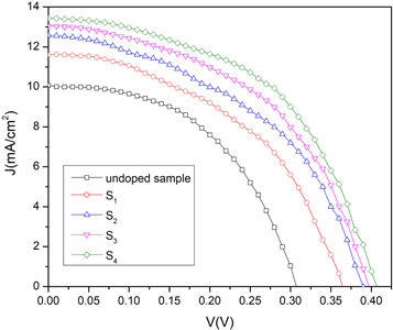
The J-V characteristic property of specimens under AM1.5 illumination is shown in figure 11. The photovoltaic parameters such as efficiency, short circuit current density (JSC), open-circuit voltage (VOC) and filling factor (FF) are calculated by using following relations [47] and listed in table 5.


As can be seen, the efficiency of samples is increased from 1.53% for the undoped sample to 2.78% for the highest doped sample, sample S4. The value of JSC is increased from 10.07 to 13.43 mA cm−2, which can be due to the enhancement of photocarriers concentration caused by Ag-doping. The trap levels in the band gap are increased by silver doping. Incident photons can excite electrons from the trap levels to the conduction band and increase the photocarriers concentration. Also, the increase of JSC incorporated can be attributed to the reduction of compressive micro-strain and dislocation density, increasing the crystallite size and decrement of barrier height between the electrode and CdSe thin films as the result of silver-doping [41] The results show that Ag-doped CdSe thin films are a promising candidate to use as an absorber layer in semi-transparent thin film solar cells.
Figure 11. I-V characteristic curves of the FTO/CdSe/Al devices under illumination condition.
Download figure:
Standard image High-resolution image
Table 5. Photovoltaic parameters of the FTO/CdSe/Al devices.
| Sample | JSC (mA/cm2) | VOC (V) | FF | η (%) |
|---|---|---|---|---|
| Undoped | 10.07 | 0.31 | 0.49 | 1.53 |

|
11.6 | 0.36 | 0.47 | 1.95 |

|
12.58 | 0.39 | 0.46 | 2.24 |

|
13.05 | 0.4 | 0.48 | 2.51 |

|
13.43 | 0.41 | 0.51 | 2.78 |
3.4. Conclusion
In this work, a novel, facile and inexpensive method was used to dope silver into thermally evaporated CdSe thin films, and structural, optical, electrical and photovoltaic properties of samples were investigated as a function of doping concentration. In summary, the surface homogeneity of CdSe thin films was improved with Ag-doping. The hexagonal structure of CdSe thin films didn't change with Ag-doping. Crystallite size, micro-strain and dislocation density of specimens were studied as a function of doping concentration. The transmittance spectra were measured at the wavelength range of 400–2500 nm. The optical energy band gap was decreased (from 1.96 eV to 1.67 eV), and Urbach energy was increased (from 150 meV to 291 meV) as the result of Ag-doping. Rectification behavior in I-V characterization of samples revealed that thermionic emission is the dominant conduction mechanism. The photovoltaic efficiency of FTO/CdSe:Ag/Al samples improved from 1.53% to 2.78% by Ag-doping. Obtained results suggest that silver-doped CdSe thin films are a promising candidate to use as an absorber layer in semi-transparent solar cells and colorful photovoltaic windows.
Acknowledgments
The authors acknowledge the Ferdowsi University of Mashhad for supporting this research via the Grant No. 3/46721. One of authors wants to acknowledge Dr Nasrin Azad for good discussion.