
Abstract
Undoped and ytterbium-doped ZnO films were synthesized on fluorine-doped tin oxide (FTO) conductive substrates using zinc nitrate hexahydrate (Zn(NO3).6H2O), sodium hydroxide (NaOH), ytterbium nitrate penta-hydride (Yb (NO3)3.5H2O) as sources of Zn2+, O2− and Yb2+ ions respectively through electrodeposition method. The structure, elemental composition, and optical features were determined via x-ray diffractometry (XRD), Energy dispersive x-ray spectroscopy (EDX), UV–visible spectrophotometry (UV–vis), four-point probe technique, and scanning electron microscopy respectively. The impact of Yb on ZnO crystallographic, elemental, optical, and energy band gap features of the ZnO materials have been studied. Structural results revealed polycrystalline films while the EDX spectrum affirms the presence of the basic elemental composition of deposits. The optical result showed high absorbance feature and decreased energy band gaps of zinc oxide films after introducing ytterbium as dopant. The energy band gap value observed for the undoped zinc oxide film which was 3.05 eV recorded a decreased range from 2.79 eV to 2.64 eV upon doping. The films exhibited increasing resistivity with thickness and granular nanocrystals distributed over the substrate surface. The low transmitting property and decreased energy band gaps of the Yb-doped ZnO films make it useful materials for solar thermal energy collectors and photovoltaic applications.
Export citation and abstract BibTeX RIS

Original content from this work may be used under the terms of the Creative Commons Attribution 4.0 licence. Any further distribution of this work must maintain attribution to the author(s) and the title of the work, journal citation and DOI.
1. Introduction
The role that energy plays in our daily activities and the world to ensure stable electricity cannot be overemphasized [1]. Although we have so many sources of energy encompassing natural forces—hydro, solar, tidal, waves, and biomass [2]; technological means for utilizing energy from coarse to refined methods should be developed to attain the expected outcome. Recently, solar energy researchers aim at finding novel conversion systems with high efficiency, low cost, durability; and solar materials having optical absorption that is wavelength-dependent [1]. To accomplish that, solar cells comprising of polycrystalline thin films like CdO [3], ZnO, CuO, Cu2O, and PbO alongside non-silicon materials which are reasonably cheap and conveniently obtainable are being used [4–6]. Among these metal oxides, ZnO is a potential candidate for converting energy from solar to electrical energy because it has exceptional optical and electrical properties [7], large direct band gap of approximately 3.2–3.5 eV that exhibits low production cost, non-toxicity [8–11], and higher transparency [12–15].
ZnO can be applicable in UV-light devices, light-emitting diodes, laser systems, gas sensors, electrodes in solar cells, window layers, solar cells, photocatalysis, band pass filters etc [1, 12, 16–18]. Undoped ZnO materials may be unsteady due to absorption and chemisorption which alter the surface conductance [19]. The structure, morphology, electrical, and optical features of thin ZnO materials could be enhanced via the use of elemental dopants like In, Al, Yb, B, Cu, Sn, Mn, etc [19, 20]. Also, the incorporation of dopants (like Yb) onto ZnO is capable of making the ZnO extremely conducting by narrowing its large band gap [21]; thereby making them alternative and inexpensive transparent conducting layers for solar energy conversion [22–29].
Several deposition methods such as sol-gel [7, 13, 15], chemical bath deposition (CBD) [1, 18], successive ionic layer adsorption and reaction (SILAR) method [12], spray pyrolysis [14, 16], electrodeposition (ECD) [30] etc have been utilized in synthesizing ZnO films. Amongst these techniques, electrodeposition (which is the technique used in this study) is one of the electrochemical growth methods which is well known for the fabrication of metallic thin film materials due to its affordability and simplicity. It is also a more environmentally friendly method than most chemical deposition methods that require hazardous solvents and reactive precursors [31–33].
In this paper, undoped and ytterbium-doped zinc oxide films at different percentage concentrations (0.01, 0.02, 0.03, and 0.04 mol%) were synthesized on an FTO conductive glass using electrodeposition technique as doping electrochemically synthesized zinc oxide films with ytterbium has not been reported to the best of our knowledge. The effects of Yb-dopant on the structure, elemental, optical, and energy band gap features of the ZnO deposits have been studied.
2. Experimental section
2.1. Materials and method
Fluorine-doped tin oxide (FTO) substrates were ultrasonicated for 25 min, washed in deionized water, and oven-dried. The chemicals used were graded analytically and include zinc nitrate hexahydrate (Zn(NO3)2.6H2O), sodium hydroxide (NaOH), hydrogen chloride (HCl), ytterbium nitrate pentahydrate (Yb (NO3)3.5H2O). The deposition bath was made up of the cation source (Yb (NO3)3.5H2O, Zn(NO3)2.6H2O for Yb2+, Zn2+), the anion source (sodium hydroxide for O2−), and deionized water in a 150 ml beaker while stirring the bath with a magnetic stirrer. The source of power supply was DC voltage, the glass slide was the cathode and a carbon electrode was the anode. The voltage drop through the film sample was measured after 15 s with the help of a digital multimeter while the power supply was kept at a constant voltage of 10 V. Therefore, uniform deposition was achieved using the electrochemical deposition (ECD) setup illustrated in figure 1 with the working, reference, and counter electrodes represented respectively as the deposited film (yb/ZnO), Ag/AgCl, and carbon.
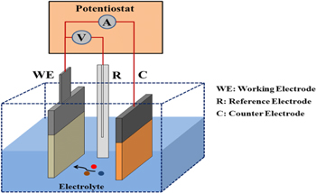
Figure 1. Schematic set-up of the electrochemical deposition adopted.
Download figure:
Standard image High-resolution image2.2. Synthesis of ZnO and Yb/ZnO thin films
Fluorine doped tin oxide (FTO) glass slides were kept in an air-tight container. 0.1 mol solution of Zn(NO3)2.6H2O and 0.01 mol solution of sodium hydroxide each was put in 150 ml of water and stirred. However, ytterbium compounds were stirred in 150 ml of deionized water for three minutes to form a colorless precursor. The coated glass slides having a dimension of 2.5 cm × 1.5 cm were used as the working electrodes. The substrates were weighed prior to depositing the ZnO and Yb/ZnO films. ECD technique was used for the deposition of ZnO and Yb/ZnO films. For the synthesis of ZnO films, 150 ml of 0.1 mol of Zn(NO3)2.6H2O was mixed with 150 ml of 0.01 mol of sodium hydroxide. For the synthesis of ytterbium dopant, Yb(NO3)3.5H2O was added to 150 ml of 0.1 mol of Zn(NO3)2.6H2O and NaOH. The undoped, 0.01, 0.02, 0.03, and 0.04 mole percentages of dopant concentrations for the Yb/ZnO samples were labelled as ZnO, Yb/ZnO 0.01 mol/%, Yb/ZnO 0.02 mol/%, Yb/ZnO 0.03 mol/% and Yb/ZnO 0.04 mol/%. The system consisted of three electrodes: the anode (platinum mesh), a working electrode/cathode, and Ag/AgCl as the reference electrode. The substrate was vertically put with the counter and reference electrodes during the synthesis. The synthesis was done at a potentiostatic condition of −200 mV versus SCE for 60 s and at a constant potential of 10 V. The synthesized films were cleaned and dried after deposition. During the syntheses processes of doping the films, 20 ml of zinc and sodium solutions, and 10 ml for dopant (Yb) solution were measured into a beaker. After the synthesis process, the samples were annealed at 200 °C for 25 min for possible removal of moisture. The chemical equations involved in the synthesis process are outlined in equations (1)–(3):


2.3. Characterization of the films
Bruker D8 Advanced x-ray diffractometer with Cu-Kα line (λ = 1.54056 Å) in 2θ range from 20°–80° was adopting in studying the films crystal features; while the surface morphologies were obtained from Zeiss Scanning Electron Microscope. Energy dispersive x-ray spectroscope was adopted in obtaining the elemental features; four-point probe measured the electrical properties while Schimadzu UV-1800 visible spectrophotometer revealed the optical properties and thickness values of the synthesized films.
3. Results and discussion
3.1. Structural analysis
Figure 2 reveals XRD plots of the ZnO and Yb-doped ZnO films respectively. The plots show the hexagonal phase of wurtzite structure of the undoped and doped ZnO films as singly represented. The existence of defined and prominent peaks for all the films confirmed their efficient and polycrystalline nature of the synthesized materials [21]. Several diffraction peaks were obtained for the Yb-doped ZnO films at 2θ angles of 31.9°, 34.4°, 36.3°, 48.0°, 57.7°, 62.9°, 66.4°, 68.4°, 73.4°, and 77.0° which also corresponded to (100), (002), (101), (102), (110), (103), (200), (201), and (202) planes respectively. It was also seen that the magnitude of the diffraction peaks of the undoped ZnO increased greatly when doped with Yb. This means that the decreased surface energy when Yb is substituted at Zn spots led to more notable preferential orientation at the (100) plane [22]. Furthermore, the increased intensity of the diffraction peaks and the dictation of more observable peaks upon ytterbium doping in figure 2 is evidence of the advancement in the crystallinity of the films [34].
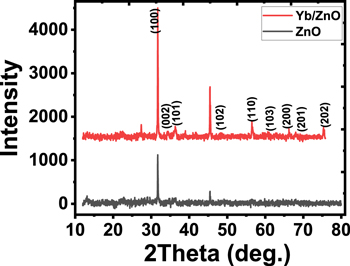
Figure 2. XRD plots of the deposited (a) ZnO and (b) Yb-doped ZnO films.
Download figure:
Standard image High-resolution imageThe crystalline size (D) was approximated from peaks broadening using Scherrer's equation in equation (4) [22, 35]:

Where k is shape factor (0.9), λ is wavelength of the radiation, β represents full width at half maximum (FWHM) of (100) plane, and θ stands for Bragg's diffraction angle in degrees. Substituting the data into Scherrer's formula gave the mean crystallite size of the deposited films. The undoped ZnO film recorded a D-value of 2.627 nm which increased to 5.732 nm upon doping with ytterbium. The dislocation density (δ) was estimated from equation (5) [22, 36]:

Some structural parameters of the undoped and ZnO materials doped with Yb is summarized in table 1.
Table 1. Structural values for the undoped and Yb-doped ZnO films.
| Sample | 2θ (degree) | Spacing d(Å) | Lattice constant (Å) | FWHM, β | hkl | Crystallite Size, D (nm) | Dislocation density, δ m2 |
|---|---|---|---|---|---|---|---|
| ZnO | 31.90 | 2.802 | 4.854 | 0.31449 | 100 | 2.627 | 1.448 |
| 48.00 | 1.893 | 3.787 | 0.15169 | 102 | 5.732 | 3.042 | |
| 57.70 | 1.596 | 3.192 | 0.55303 | 110 | 1.640 | 3.717 | |
| Yb/ZnO | 31.90 | 2.803 | 4.854 | 0.31449 | 100 | 2.627 | 1.448 |
| 48.00 | 1.893 | 3.787 | 0.15169 | 102 | 5.732 | 3.042 | |
| 57.70 | 1.596 | 3.192 | 0.55303 | 110 | 1.640 | 3.717 | |
| 68.40 | 1.370 | 3.064 | 0.29319 | 112 | 3.276 | 9.317 | |
| 73.40 | 1.288 | 3.156 | 0.16924 | 004 | 5.854 | 2.917 |
3.2. Morphological studies
The surface morphologies of the zinc oxide and ytterbium-doped ZnO films are shown in figure 3. The materials exhibited granular nanocrystals distributed unevenly and randomly over the substrate surface. The varied crystal sizes correspond with the obtained structural parameters owing to the different deposition parameters employed. The nanoclusters seen on the substrate surface enhance the absorption qualities of the synthesized materials [25]. The cracks encourage the penetration of the dopant into the host material. Similar nanograined morphology has also been reported [24, 27].
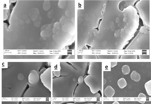
Figure 3. SEM images of the (a) undoped and (b)–(e) Yb-doped ZnO films.
Download figure:
Standard image High-resolution image3.3. Elemental studies
The elemental constituents of the undoped ZnO and Yb/ZnO films were conducted via electron dispersive x-ray spectroscopy (EDX) as showed in figure 4. Figure 4(a) shows the EDX spectra of the undoped ZnO film while the doped samples exhibited same EDX patterns as singly represented in figure 4(b). In a typical EDX spectrum, the location of the peaks confirms the presence of the basic elements while the peak height aids in the quantification of each element's concentration in the film sample [37]. The EDX result of the undoped ZnO material in figure 4 affirms the presence of zinc and oxygen with a higher intensity peak of zinc and evidence of the presence of ytterbium (Yb) for the doped samples is seen in figure 4(b).

Figure 4. EDX patterns of the (a) Undoped and (b) Yb-doped ZnO films.
Download figure:
Standard image High-resolution image3.4. Optical analysis
The absorbance (A) for ZnO and Yb-doped zinc Oxide (Yb/ZnO at 0.01, 0.02, 0.03, and 0.04 mol%) films were conducted using UV-1800 spectrophotometer (wavelength between 300–1100 nm). Absorbance measurements of all the films (undoped and Yb doped) were observed to have good absorption at short wavelength region (ultraviolent) but started decreasing with an increase in wavelength as shown in figure 5(a). Similar absorbance trend has been recorded in literature [38]. It was also observed that an increase in Yb doping concentration increased the absorption spectrum except for the Yb/ZnO 0.01 mol% film. Using the absorbance measurement, the other optical features of the materials have been analyzed.
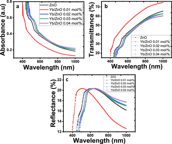
Figure 5. Plots of (a) absorbance (b) transmittance and (c) reflectance against wavelength for the deposited films.
Download figure:
Standard image High-resolution imageThe transmittance and reflectance values were deduced from the absorbance data using the following relations in equations (6), (7) [36]:

Where Transmittance is T, Absorbance is A, and Reflectance is R.

Figure 5(b) shows the transmittance graph of undoped and Yb/ZnO materials. The transmittance of the films decreased in the UV region and increased with increase in wavelength up to the NIR of the electromagnetic spectrum. The transmittance of undoped and Yb/ZnO 0.01 mol/% films exhibited an average of nearly 70% and decreased at increasing Yb concentrations. Resembling trend of increase in transmittance was also discovered by Manoharan et al [22] for Al-doped ZnO. The decrease in optical transmittance of ZnO after introducing Yb-dopant could be attributed to the enhanced grain boundaries while introducing the dopant [39]. These films can serve as galvanizing material coatings to avert corrosion in a couple of material surfaces. Also, because of its low transmittance when doped with a high concentration of Yb, it can be used for solar thermal energy collector and active layer for solar cell application [2]. Figure 5(c) shows the reflectance plots of the films. The materials recorded their maximum reflectance value of approximately 20% in the UV region of the spectrum which reduced at increasing wavelength. The estimated values for absorbance, transmittance, and reflectance of all the films at 700 nm wavelength are summarized in table 2. The optical shifts could be due to ytterbium introduction and the thermal treatment prior to deposition.
Table 2. Estimation of some optical parameters of the ZnO and Yb/ZnO films.
| Sample | Absorbance (a u) | Reflectance (%) | Transmittance (%) |
|---|---|---|---|
| ZnO | 0.312 | 19.85 | 60.91 |
| Yb/ZnO 0.01mo% | 0.221 | 17.47 | 46.00 |
| Yb/ZnO 0.02 mo% | 0.342 | 20.03 | 47.98 |
| Yb/ZnO 0.03 mo% | 0.342 | 20.03 | 47.98 |
| Yb/ZnO 0.04 mo% | 0.342 | 20.03 | 47.98 |
The reliance of absorption coefficient, α on the photon energy (hv) gives the insight in respect to the form of optical shift which happens within the valence and conduction band of a material [40]. The absorption coefficient, α is given by transmittance, T and the material thickness, d as shown in equation (8) [41];

Figure 6(a) displays the graph of absorption coefficient (αhv against hv). It has been confirmed that when a photon falls on a surface, transmission, reflection, and absorption occurs [42]. Absorption coefficient  gives insight on the extinction coefficient k, which measures the amount of light lost when scattering and absorption per unit distance of the penetration medium occurs [40] and is related in equation (9) as [18, 43];

Where α represents optical absorption coefficient and λ is wavelength. Refractive index is the ratio of the speed of radiation in one medium to that in another medium. It plays a lead role in optical material search and in constructing anti-reflecting coatings for solar cells [44]. According to Nwofe and Agbo [18], optical reflectance has a relation with refractive index, n which is given in equation (10);

Where n = refractive index and R = optical reflectance.
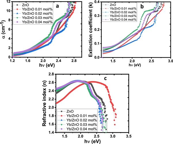
Figure 6. Plots showing the (a) absorption coefficient (b) extinction coefficient (c) refractive index of the deposited films.
Download figure:
Standard image High-resolution imageFigures 6(b) and (c) gives extinction coefficient and refractive index versus photon energy plots respectively for the ZnO and Yb/ZnO films at varying percentage concentrations (0.01–0.04 mol%). In figure 6(b), the extinction coefficient increases with a rise in photon energy for all the deposited materials. The ZnO samples with a high concentration of Yb dopant (0.03 and 0.04 mol%) recorded high extinction values when compared to the samples deposited at 0.01, 0.02 mol%, and undoped ZnO. This increase in extinction value for samples with high Yb concentration can be associated with a decrease in transmittance and a rise in the absorption coefficient. These films can be very useful in solar cell fabrication. Figure 6(c) indicated that the refractive index, n dropped with rise in photon energy which revealed typical dispersion behaviour of the material.
Optical conductivity  is the optical feedback of a transparent solid. It is given by the relation in equation (11) [45];

Where c = speed of light, α = absorption coefficient and n = refractive index. The graph of  versus hv for undoped and Yb/ZnO films are shown in figure 7(a). It reveals that optical conductivity,
  increased with a rise in hv for all the materials. It was also observed that the introduction of high Yb dopant concentrations (0.03 and 0.04 mol%) has a prominent effect on the optical conductivity of the materials. It tends to raise the conductivity of the films which indicates that they have good photo-response and could be employed as photoconductors [46]. Such films are good candidate materials for thin-film solar cell fabrication and various optoelectronic device applications [32].
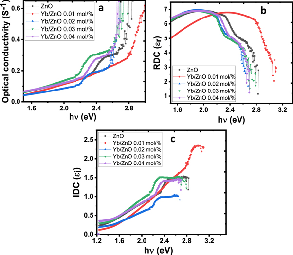
Figure 7. (a) Optical conductivity (b), (c) real and imaginary dielectric constant plots of the synthesized films.
Download figure:
Standard image High-resolution imageThe dielectric constant  can be defined as a foundational inherent attribute of the material. It has two parts: the real dielectric part
  which is affiliated to the word that uncovers the extent that the speed of light would be bridged within the material while the imaginary dielectric part
  reveals how a dielectric material will take in energy from an electric field because of dipole movement [18]. Dielectric (real and imaginary) constants in equations (12), (13) can be evaluated from 'n' which stands for refractive index and k (extinction coefficient) given the following mathematical relations [47, 48]: For the real dielectric part;

For imaginary dielectric part;

Figures 7(b) and (c) gives the plots of real dielectric constant (RDC) and imaginary dielectric constant (IDC) against hv, the description of the real dielectric part with respect to hv is related to refractive index due to the minuscule value of k2 in comparison to n2, while the imaginary dielectric part depends both on n and k. In this study, the real dielectric values are higher as compared to the imaginary dielectric values. Figure 7(b) reveals that the real dielectric constant of all the film samples tends to exhibit a similar trend, they increase with a rise in photon energy up to 2.2 eV and then decreases drastically as the photon energy increases while figure 7(c) reveals that the imaginary dielectric increases as the photon energy rises and then keep constant value above 2.4 eV except for Yb/ZnO 0.01 mol% that increases almost linearly with the photon energy.
3.5. Energy band gap (Eg)
Intrinsic absorption that correlates to exciting electrons out of the valence band to conduction band, could be utilized to obtain the energy band gap nature [49]. The energy band gap, Eg of the deposited materials were determined through equation (14) given as [2, 50];

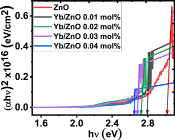
For allowed direct transitions, where absorption coefficient ( ), Planck's constant (h), frequency (v), energy band gap (Eg) and A is constant that is material reliant. The energy band gap of the materials were gotten over extrapolating the linear part of the curve
  in a graph of
  against hv as seen in figure 8 [7, 51]. It was observed that the introduction of Yb dopant improved the energy band gap nature of ZnO because of the surplus concentration of carriers at the conduction band of ZnO. The synergy among free carriers arising from a high percentage concentration of Yb gives rise to a reduction in the energy band gap as shown in figure 8. A similar band gap change was obtained by Kamarulzaman et al [52] and Varughese et al [53]. The energy band gap values deduced from the graph have been outlined in table 3 with their corresponding thickness values. It was discovered that the material thickness increased with a decline in the energy band gaps for all the samples. A related descending trend in band gap has been recorded by Rahman et al [54] and Nwanya et al [12].
Figure 8. Energy band gap plots for the synthesized samples.
Download figure:
Standard image High-resolution image
Table 3. Energy band gap, thickness, and electrical values of the film samples.
| Sample | Thickness (nm) | Eg (eV) | Resistivity, ρ (Ωcm) × 103 | Conductivity, σ (Ωcm)−1 ×10⁻⁴ |
|---|---|---|---|---|
| ZnO | 105.98 | 3.05 | 5.424 | 1.843 |
| Yb/ZnO 0.01 mo% | 110.85 | 2.79 | 5.650 | 1.769 |
| Yb/ZnO 0.02 mo% | 112.56 | 2.70 | 5.771 | 1.732 |
| Yb/ZnO 0.03 mo% | 114.86 | 2.68 | 5.892 | 1.697 |
| Yb/ZnO 0.04 mo% | 118.74 | 2.64 | 5.910 | 1.692 |
3.6. Electrical studies
The electrical parameters of the synthesized materials were measure using four-point probe technique at room temperature using Keithley 2400 source meter. The obtained electrical resistivity and conductivity values of the undoped and ytterbium-doped zinc oxide films have been outlined in table 3. Table 3 reveals increased resistivity of the synthesized materials with increasing thicknesses and decreasing electrical conductivities. This result confirms the obtained band gap energies which decreased as the molar percentage of ytterbium increased. Similar results have been obtained upon ytterbium doping [24].
4. Conclusion
Undoped and ytterbium-doped zinc oxide (0.01, 0.02, 0.03 and 0.04 mol%) films have been deposited successfully on an FTO substrates using zinc nitrate hexahydrate (Zn(NO3).6H2O), sodium hydroxide (NaOH), ytterbium nitrate penta-hydride (Yb(NO3)3.5H2O) as a source of Zn2+, O2-, and Yb2+ ions respectively through electrodeposition technique. The structure, composition of elements, and optical features has been studied via x-ray diffractometry (XRD), energy dispersive x-ray spectroscopy (EDX) and UV-vis spectroscopy accordingly. The influence of Yb-dopant on the crystallographic, optical and band gap energy features of ZnO were investigated and it was observed to improve the features of the ZnO films. XRD result reveals the presence of well-defined peaks for all the films which confirmed their polycrystalline nature. The structural result also revealed that the Yb dopant increased the intensity of the preferred orientation along (100) plane while the dictation of more observable peaks enhanced the crystallinity of the films. The elemental constituents obtained from EDX affirmed deposition of Zn, O and Yb and their quantity in the deposited films. The material thickness was observed to increase with higher Yb dopant concentration from 105.98 nm to a maximum value of 118.74 nm. The optical studies revealed high transmittance and decreased band gap energies of the zinc oxide after introducing ytterbium as dopant. Energy band gap of 3.05 eV was obtained for the undoped zinc oxide but decreased to 2.64 eV upon doping with different concentrations of ytterbium. Electrical studies showed increasing resistivity values and decreasing conductivity with thickness while surface morphology studies exhibited granular nanocrystals over the substrate surface. These films can serve as galvanizing materials to avert corroding effect when coated in a couple of material surfaces. Also, because of its high transmittance and reduced band gap energy when doped with ytterbium, it can be used as potential materials in solar thermal energy collector and as an active layer for solar cell application.
Data availability statement
All data that support the findings of this study are included within the article (and any supplementary files).