
Abstract
The low dielectric constant of organic semiconductors has been a limiting factor in the organic photovoltaics. Non-Fullerene Acceptor Bulk Heterojunction (NFA-BHJ) organic solar cells with high dielectric constant acceptors have been gaining a lot of attention. No simulation work has been done on NFA-BHJ organic solar cell with a high dielectric constant acceptor so far to study the influence of various material parameters on the device performance. In this work, a comprehensive device modelling of the conventional structure of NFA-BHJ with poly[(2,6-(4,8-bis(5-(2-ethylhexyl)thiophen-2-yl)benzo[1,2-b:4,5-b']dithiophene)-co-(1,3-di(5-thiophene-2- yl)-5,7-bis(2-ethylhexyl)benzo[1,2-c:4,5-c']dithiophene-4,8-dione)] (PBDB-T)as the polymer donor and (3,9-bis(2-methylene- (3-(1,1 -dicyanomethylene)-indanone)-5,5,11,11-tetraki(4-hexylphenyl)-dithieno [2,3-d:2,3-d]-s-indaceno [1,2-b:5,6-b]dithiophene)) with Oligo-Ethylene side chain (ITIC-OE) as the non-fullerene acceptor is performed. We did a detailed analysis on the impact of technological parameters on the cell performance and optimized the device characteristics to produce improved efficiency. Numerical simulation is done using SCAPS 1-D program and the validity of simulated output has been verified by comparing with the measurements from reported literature. Optimization of the device parameters produced an improved device performance with an open circuit voltage of 0.9562 V , short circuit current density of mA cm−2 , Fill factor of 69.75% and a power conversion efficiency of 11% . The results are encouraging to develop NFA-BHJ organic solar cells with high dielectric constant acceptors in the near future.
Export citation and abstract BibTeX RIS

Original content from this work may be used under the terms of the Creative Commons Attribution 3.0 licence. Any further distribution of this work must maintain attribution to the author(s) and the title of the work, journal citation and DOI.
1. Introduction
Organic solar cells(OSC) have shown a lot of potential over the last few years thanks to the ease of material availability as well as low cost, along with improved efficiency [1–4]. Since 2000s, Bulk heterojunction solar cells with polymer donors and fullerene acceptors have been showing tremendous improvement [5]. The 3-D conjugated cage structures of fullerene acceptor molecules allowed them to have better device performance, but the contribution of acceptor layer to the photocurrent is limited [6–9]. An attractive alternative is the use of Non-Fullerene acceptor which overcomes the morphological instability and poor optical properties of fullerenes [10–18]. However, the relatively low dielectric constant( r) values of the organic semiconductors have been a limitation for organic solar cell due to their high exciton binding energy [19–24].
Studies show that an improved r can provide better device performance with reduced charge carrier recombination along with providing more efficient charge separation pathway for the donor-acceptor interface,thus enhancing the short circuit current density and fill factor[20–2420-24].ITIC (3,9-bis(2-methylene- (3-(1,1 -dicyanomethylene)-indanone)-5,5,11,11-tetraki(4-hexylphenyl)-dithieno [2,3-d:2,3-d]-s-indaceno [1,2-b:5,6-b]dithiophene)) is one of the dominant acceptor in Non-Fullerene Acceptor Bulk Heterojunction (NFA-BHJ) OSC [25–28]. It is reported in literature that Oligoethylene(OE) side chain improves the r of organic semiconductors [29–33]. Addition of OE side chain to ITIC results in acceptor of r = 9, much larger than ITIC [34]. Being an ITIC derivative with OE side chain, the optical properties are same to that of ITIC with significant improvement in the dielectric constant due to the better orientations of dipole moments originating from the additional side chain [29]. The improved r value reduces the energy gap between singlet-triplet system, effectively blocking the recombination of charge carriers [20, 35].
An experimental work on NFA-BHJ with ITIC-OE acceptor has been recently reported in the literature [34].Device modelling is an efficient tool to understand the device operation and for optimizing the NFA-BHJ [36].Since there is no computational work available for non-fullerene BHJ solar cell with ITIC-OE acceptor, the simulations can provide the necessary prerequisites for the high r acceptor to become an important part of organic solar cell research.
Solar cell capacitance simulator (SCAPS) is widely used to simulate various types of solar cells including NFA-BHJ [36–44]. The calibration of software can be done using control variable method and the experimental work can be reproduced successfully. In this work, SCAPS is used to numerically simulate NFA-BHJ OSC with PBDB-T (poly[(2,6-(4,8-bis(5-(2-ethylhexyl)thiophen-2-yl)benzo[1,2-b:4,5-b']dithiophene)-co-(1,3-di(5-thiophene-2-yl)-5,7-bis(2-ethylhexyl) benzo [1,2-c:4,5-c'] dithiophene-4,8-dione)]) as the polymeric donor and ITIC-OE as the NFA acceptor having PEDOT : PSS as the hole transport layer(HTL) and PFN-Br as the electron transport layer (ETL) . A comprehensive device modelling is done for NFA-BHJ OSC to study the influence of the technological parameters on the output performance of the organic solar cell.
2. Numerical modelling and material parameters
One dimensional Solar Cell Capacitance Simulator-SCAPS version (3.3.06) has been used as the numerical simulation tool. It solves both the electrical model and optical model over the entire configuration. The experimental work on PBDB-T/ITIC-OE is simulated in SCAPS 1-D under AM 1.5 G Spectrum and material parameters are calibrated using control variable method.
The configuration of the simulated bulk heterojunction structure is Glass substrate/ITO/PEDOT : PSS/ PBDB-T/ITIC-OE/PFN-Br/Ag as shown in figure 1. along with the energy band diagram. The material parameters used in the simulation are depicted in table 1. The given parameters Eg is the energy bandgap,r is the relative permittivity, χ being the electron affinity, μn and μp are the electron and hole mobilities,Nt is the defect density respectively. NA and ND are the densities of acceptor and donor materials whereas NC and NV are the effective densities of conduction band and valence band. Identical values are used for parameters not mentioned in the table such as neutral Gaussian distribution of defect density with the characteristic energy set to 0. 1 eV. Additionally, electron and hole thermal velocity is set to 107 cm s−1.The electron and hole capture cross section is taken to be 9 × 10⁻¹⁵ cm2. The work function of anode is set at 4.7 eV [45] and cathode is set at 4.1eV. The interface defect density has been set to 2 × 109 cm−2 where the defect interfaces are HTL/Active and Active/ETL. The dielectric constant of active layer is obtained by averaging the values of r of donor and acceptor materials [34] and the energy gap is optimized to fit the simulated data [46].The absorption profile is taken from the experimental work on PBDB-T/ITIC-OE [34].The optimized parameters are fed into the SCAPS simulator with no optical reflectance being considered.
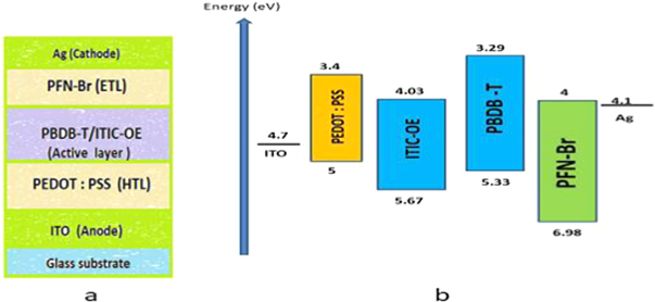
Figure 1. Simulated solar cell (a) configuration of the cell (b) Enegy band alignment.
Download figure:
Standard image High-resolution imageTable 1. Numerical parameters used in the simulation.
| Parameters | HTL | Active layer | ETL |
|---|---|---|---|
| Thickness(nm) | 40 [34] | 100 [34] | 5 [34] |
| Eg(eV) | 1.6 [47] | 1.2 [46] | 2.98 [48] |
| χ(eV) | 3.4 [47] | 4.03 [34] | 4 [36] |
| r |
3 [47] | 6.1 [34] | 5 [36] |
| μn(cm2/vs) | 4.5 × 10⁻⁴ [36] | 1.2 × 10⁻⁵ [34] | 2 × 10⁻⁶ [36] |
| μp(cm2/vs) | 9.9 × 10⁻⁵ [36] | 3.5 × 10⁻⁴ [34] | 1 × 10⁻⁴ [36] |
| NA(cm−3) | 2 × 10¹⁸ | 0 | 0 |
| ND(cm−3) | 0 | 7.5 × 10¹⁸ | 9 × 10¹⁸ |
| NC(cm−3) | 1022 [47] | 1019 | 1019 [36] |
| NV(cm−3) | 1022 [47] | 1019 | 1019 [36] |
| Nt(cm−3) | 109[36] | 1012 | 109 [36] |
The simulated solar cell output parameters; Open circuit voltage(Voc), Short circuit current density(Jsc),Fill Factor(FF) and Power Conversion Efficiency(PCE) are compared with the experimental result as in table 2. The results are in close agreement with the experimental values, thus validating the simulation and demonstrating that SCAPS software is perfectly calibrated for non-fullerene organic solar cells.
Table 2. Comparison of simulated output with experimental result.
| Experimental | Simulated | |
|---|---|---|
| Voc(V) | 0.85 | 0.8491 |
| Jsc(mA/cm2) | 14.8 | 14.616 |
| FF(%) | 67 | 66.88 |
| PCE(%) | 8.5 | 8.3 |
The illuminated current density-voltage(J-V) curve and External Quantum Efficiency (EQE)curve are shown in figure 2. and are consistent with the experimental results of non-fullerene organic solar cells [34]. It shows that the input parameters are extremely close to the real parameters of the device. The calibrated cell is simulated to analyse the impact of material parameters on the output and enhancing the PCE by optimizing the input values.
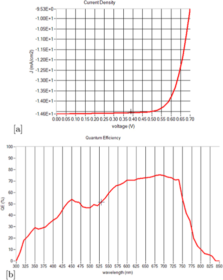
Figure 2. Simulated output from SCAPS (a) J-V curve and (b) EQE curve.
Download figure:
Standard image High-resolution image3. Results and discussion
3.1. Effect of active layer thickness
The non-fullerene OSC is simulated at different active layer thickness ranging from 50 nm to 250 nm and the variation of output parameters with the thickness is studied as given in figure 3.
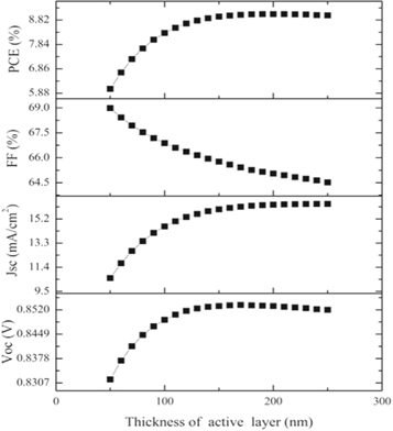
Figure 3. Effect of active layer thickness on output parameters.
Download figure:
Standard image High-resolution imageOn increasing the thickness of active layer, Voc increases slightly until 200 nm and starts to decrease on further increase, Voc depends on the dark saturation current and it is decreased at higher thickness [49]. But the rate of decay is low for values above 220nm making it the optimized input value for Voc. It is seen in literature that the ITIC-OE based devices have dominant monomolecular and or/ trap-assisted recombination mechanisms owing to the blend morphology [34].
The Jsc and PCE shows a steady increase with peak values of 16.38 mA cm−2 and 9.06% respectively at 220 nm. On further increasing the thickness, Jsc and PCE starts to decrease . The improvement in PCE and Jsc can be attributed to the increased charge generation on increasing thickness. The active layer thickness of a photovoltaic cell should be in agreement with the exciton diffusion length.As the thickness increases beyond 220 nm,the diffusion length becomes lesser than the active layer thickness and the generated electron-hole pairs are recombined before undergoing charge separation. The fill factor significantly drops from 68.99% to 64.43% on increasing the thickness indicating that the series resistance of non-fullerene organic solar cell increases with the active layer thickness as already reported [35].
3.2. Effect of defect density of the active layer
The effect of defect density on the output performance of solar cell is studied using the SRH recombination model [50] with the equation being:

where n, p refers to the mobile electron-hole concentration, and nt,pt being the trap defect concentration with ni,the intrinsic concentration. The lifetime τ is given by the relation [51]:

with σ being the capture cross section and Nt, the trap defect density and Vth being the carrier thermal velocity. The exciton diffusion length is given by  where D is the diffusion constant.
equations indicate that on increasing Nt ,the lifetime τ decreseas thereby reducing the diffusion length and leads to high recombination rate. The simulated values of diffusion length and lifetime by setting the same parameters for electron and hole are given in table 3.
Table 3. Variation of diffusion length and lifetime of electron with defect density.
| Nt(cm−3) | 1010 | 1011 | 1012 | 1013 | 1014 |
|---|---|---|---|---|---|
| Ln(μm) | 0.19 | 0.059 | .019 | .0059 | .0019 |
| τn(μs) | 1100 | 110 | 11 | 1.1 | 0.11 |
As shown in figure 4., on increasing Nt from 1010 to 1011 cm−3, the output parameters fall off drastically in agreement with the equation (1).The PCE shows a drop from 9.17% and 1.19% significantly, we have set the calibrated value of Nt at 1012 cm−3,since the diffusion length corresponding to 1011 cm−3 cannot be realised in experiment [51].
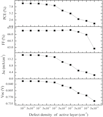
Figure 4. Effect of defect density of active layer on output parameters.
Download figure:
Standard image High-resolution image3.3. Effect of doping density of active layer
The performance of BHJ organic solar cell as a function of doping density is already reported in literature [52]. We studied the influence of doping concentration on non-fullerene BHJ by changing the value from 1017 to 1020cm−3 as shown in figure 5. Voc changes only slightly while the Jsc value drops from 15.994 mA cm−2 to 13.5 mA cm−2. It can be attributed to the degradation of cell performance while optimised BHJ doping reduces the electric field of active layer; FF and PCE shows steady increase upon improved doping density which can be due to unbalanced charge carrier mobilities. The doping increases the cell performance by compensating for the space charge created by slower carriers and reducing the recombination of free carriers [52].
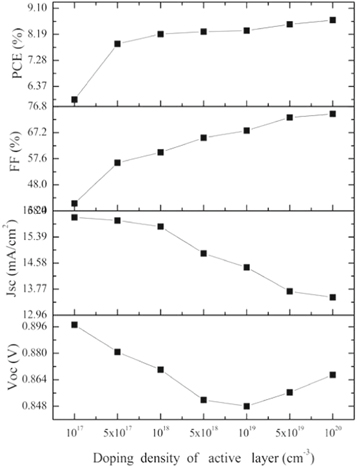
Figure 5. Effect of doping density of active layer on output parameters.
Download figure:
Standard image High-resolution image3.4. Effect of defect density at interface layers
Two defined interfaces are Active/ETL and and HTL/Active. The defect densities of two interfaces have been increased from 107 cm−2 to 1011 cm−2 to study the effect on output parameters. As already seen in figures 6 and 7., defect densities will provide more traps leading to lower cell performance. The effect is shown only at the HTL/Active interface where FF and Voc shows significant drop leading to lower PCE while Jsc is decreased only slightly upon increasing the interface defect density. But, when we consider the Active/ ETL interface, the defect density doesn't effect the cell performance at all showing consistent output except at 1010 cm−2 . This can be attributed to the fact that the illumination of the device is from the front contact in its conventional pathway and HTL/Active interface defect is dominant in the structure.
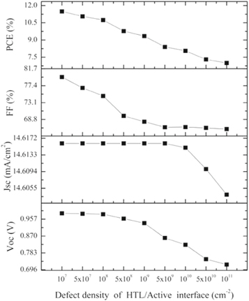
Figure 6. Effect of defect density at HTL/Active interface on output parameters.
Download figure:
Standard image High-resolution image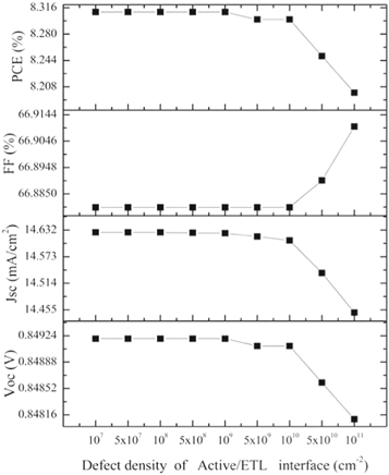
Figure 7. Effect of defect density at Active/ETL interface on output parameters.
Download figure:
Standard image High-resolution image3.5. Effect of HTL and ETL characteristics
Here, we study the effect of input parameters of HTL and ETL layers such as thickness, doping concentration, electron affinity and mobility on the solar cell performance.
The thickness of HTL layer has been varied from 30 to 50 nm as shown in figure 8, while that of ETL layer has been varied from 3 to 9 nm as in figure 9. On increasing the thickness of HTL layer, Voc is improved slightly while Jsc linearly increases until 48 nm and drops down after that. FF rather shows a unique variation with step-wise jumping at 36 nm and 46 nm, with a constant value following those. However, the variation is too small to have an impact on the output. The PCE shows a constant value upon increasing the HTL layer thickness making it clear that the transport layer doesn't effect the series resistance of non-fullerene solar cell made up of ITIC-OE acceptor. Upon increasing the ETL layer thickness, there is only a slight increase in Voc and Jsc, while a slight decrease in FF value. However, the PCE is almost constant with a negligible drop towards the end.
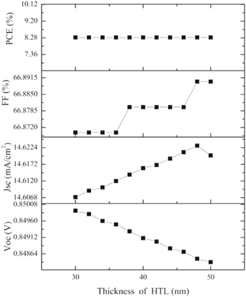
Figure 8. Effect of thickness of PEDOT:PSS on output parameters.
Download figure:
Standard image High-resolution image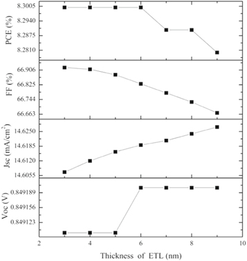
Figure 9. Effect of thickness of PFN-Br on output parameters.
Download figure:
Standard image High-resolution imageIncreasing the doping concentration of HTL results in improving the output performance of solar cell . This can be attributed to the increase in conductivity of the cell leading to a reduced series resistance. The ETL layer follows a similar trend as shown in figures 10 and 11.
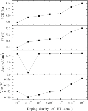
Figure 10. Effect of doping density of PEDOT:PSS on output parameters.
Download figure:
Standard image High-resolution image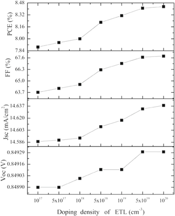
Figure 11. Effect of doping density of PFN-Br on output parameters.
Download figure:
Standard image High-resolution imageThe effect of mobility is shown in figures 12 and 13. The hole mobility of HTL layer mobility is being increased from 10−6 cm2/versus to 10−3 cm2/versus and electron mobility of ETL layer being increased from 10−7 cm2/versus to 10−3 cm2/versus. The output is similar to the one obtained on changing the doping concentration further convincing the increase in conductivity of the material due to mobility effect.
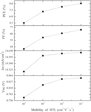
Figure 12. Effect of hole mobility of PEDOT:PSS on output parameters.
Download figure:
Standard image High-resolution image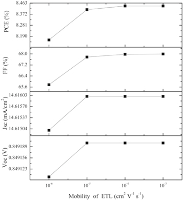
Figure 13. Effect of electron mobility of PFN-Br on output parameters.
Download figure:
Standard image High-resolution imageThe electron affinity of HTL layer is increased from 3 eV to 3.8 eV and that of ETL layer is increased from 3.7 eV to 4.3 eV. The PCE of 8.31% and 8.35% are achieved for optimum values at 3.5 eV and 4.1 eV respectively. The results are shown in figures 14 and 15. As it appears, the optimum electron affinities reduce the bandgap offset leading to a better energy alignment and helps in improved charge transport between active and transport layer of the non-fullerene organic solar cell [36].
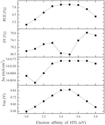
Figure 14. Effect of electron affinity of PEDOT:PSS on output parameters.
Download figure:
Standard image High-resolution image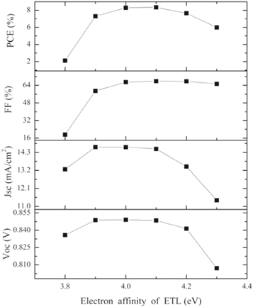
Figure 15. Effect of electron affinity of PFN-Br on output parameters.
Download figure:
Standard image High-resolution image3.6. Effect of Operating temperature
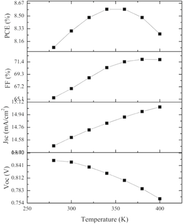
The operating temperature is varied from 280 K to 400 K for the simulation and its effect on output performance is studied . As it appears in figure 16, the increase in temperature shows a significant drop in Voc of the cell from 0.8528 V to 0.7641 V. It may be due to the increased recombination rate resulting from a higher value of saturation current. The Jsc has improved slightly due to the increase in the number of thermal carriers. FF shows a steady improvement from 65.32% to 71.83% and degrades after 360 K as a result of saturation current. PCE shows a slight improvement with a peak value of 8.59% at 340 K and degrades after that, Here the significant improvement of FF dominates over the degradation of Voc of solar cell.
Figure 16. Effect of operating temperature on output parameters.
Download figure:
Standard image High-resolution image
The optimized numerical parameters are summarized in table 4 with an improved output comprising Voc of 0.9562 V , Jsc of 16.4997mA cm−2 , FF of 69.75% and PCE of 11%. We compared the simulation results with the original experimental work in table 5.These optimizations show that PCE can be further enhanced for high dielectric constant NFA-BHJ organic solar cell in the near future.
Table 4. Optimized numerical parameters.
| Parameters | ETL | Absorber | HTL |
|---|---|---|---|
| Doping density(cm−3) | — | — | 1019 |
| Electron affinity(eV) | 4.1 | — | 3.5 |
| Thickness(nm) | — | 220 | |
| Hole mobility(cm2v−1s−1) | — | — | 5 × 10⁻³ |
Table 5. Comparison of device performance of the NFA-BHJ reported in the experimental work and simulated results using optimized numerical parameters.
| Parameters | Experiment | Simulation | Optimized thickness | Optimized χ | Optimized(NA,μp) | Final |
|---|---|---|---|---|---|---|
| Voc(V) | 0.85 | 0.8491 | 0.8531 | 0.8585 | 0.8559 | 0.9562 |
| Jsc()mA/cm2) | 14.8 | 14.616 | 16.32 | 14.569 | 14.74 | 16.4997 |
| FF(%) | 67 | 66.88 | 65.05 | 67.01 | 74.13 | 69.75 |
| PCE(%) | 8.5 | 8.3 | 9.06 | 8.38 | 9.35 | 11 |
4. Conclusion
Numerical studies on non-fullerene BHJ OSC with high dielectric constant ITIC-OE acceptor with the structure ITO/PEDOT : PSS/ PBDB-T/ITIC-OE/PFN-Br/Ag is performed. The results are verified by comparing simulated results with the experimental work reported in literature. The cell performance is in close agreement with the real device performance. We have studied the influence of thickness, doping concentration and defect density of the absorber layer, operating temperature, defect density at HTL/Active and Active/ETL intefaces, transport layer characteristics on the cell performance and optimised the parameters to improve PCE. The simulated output shows that the cell performance is significantly improved with a higher doping density due to unbalanced carrier mobilities. PCE is improved upto 220 nm thickness of active layer and it is clear from the simulated results that a lower defect density of active layer is ideal for better solar cell output. The HTL/Active interface defect density effects the cell performance while ETL/Active interface is insignificant. Higher operating temperature degraded the device performance. The transport layer characteristics are optimized in the simulation. The thickness of HTL and ETL layers have negligible influence on the PCE while optimized values of hole mobility of HTL is 5 × 10⁻³ cm2 V−1 s−1 and the doping density is 1019 cm−3. The electron affinities of HTL and ETL are optimized at 3.5 eV and 4.1 eV respectively. The cell performance with optimized numerical parameters are Voc = 0.9562 V, Jsc = 16.4997mA cm−2 , FF = 69.75% and PCE = 11%. The numerical simulation studies show that the device performance of NFA-BHJ OSC with ITIC-OE acceptor can be improved to obtain enhanced PCE through the optimization of material parameters of the cell. The studies also indicate that ITIC-OE is an ideal candidate for acceptor material in organic solar cell to achieve higher efficiencies in the near future.
Acknowledgments
Nithya K S gratefully acknowledges Kerala State Council for Science, Technology and Environmen(KSCSTE) for the financial support under KSCSTE Research fellowship Programme.