


Abstract
This work demonstrates an approach for simplifying fiber-to-chip (edge coupling) packaging by virtually eliminating the longitudinal alignment procedure (also increasing compactness and efficiency) through a fiber lens embedded into the structure of the fiber itself. A parabolic lens, fabricated using focused ion beam milling, with a diameter of 15 μm and height of 5 μm, was embedded 6.5 μm (the working distance of the parabolic lens) below the endfacet of the fiber. The lens focuses a 10.4 μm fiber mode into a spot size of 2.6 μm on the surface of an SMF-28e single-mode optical fiber. The properties of the fabricated lens were studied using the three-dimensional finite-difference time-domain numerical method, and the optimal parameters for maximizing the coupling conditions were extracted. The conversion loss of the lens is estimated to be around  . The insertion loss and lateral alignment of the proposed parabolic lens is comparable to a commercial lensed fiber, while directly ensuring the longitudinal alignment, easing the angular alignment, and providing additional mechanical and environmental robustness.
Export citation and abstract BibTeX RIS

Original content from this work may be used under the terms of the Creative Commons Attribution 3.0 licence. Any further distribution of this work must maintain attribution to the author(s) and the title of the work, journal citation and DOI.
1. Introduction
Over the past decades, mainly driven by the development of optoelectronic and photonic integrated circuits, silicon photonics has portrayed a promising potential in becoming a mainstream solution for high-bandwidth data transfer between and within microchips [1, 2]. One of the challenges in the realization of this vision relates to packaging, in particular to the coupling losses and misalignments at the interface between the optical fiber and the photonic integrated chip. The largest proportion of these coupling loses can be attributed to the mode field mismatch between the mode of the input/output optical fibers and the integrated submicron waveguides on the chip [3]. As such, it comes as no surprise that reducing this loss component has been the focus of several studies [4–12]. The main strategies that have been used for mitigating coupling losses associated with the mode field mismatch can be classified as vertical grating couplers [4–6], and edge couplers using inverted lateral tapers [7–12]. Edge couplers result in lower insertion losses (below  , compared to
  achieved for grating couplers [13]), have broadband operation, and are less sensitive to the polarization of light [3]. However, they require a fiber lens interface between the fiber and the on-chip coupler to compensate for the mismatch between the modes of the fiber and the waveguide. Some available efficient designs for fiber lenses include the use of diffractive elements [14–16], concave fiber tips [17], and gradient-index fiber lenses [18]. While these strategies have demonstrated improvements in coupling efficiency compared to bare single-mode optical fibers (around 10.4 μm mode field diameter), most still do not outperform commercial lensed fibers when coupling into submicron waveguides. In addition, none of these strategies include a practical solution to the longitudinal misalignment between the fiber and the chip coupling interface, presenting an additional challenge for accurate and low-cost packaging solutions [13]. An elegant approach towards more flexible fiber-to-chip and chip-to-chip coupling is presented in [19], using nanoprinted optical free-form elements. In a previous study, we demonstrated the application of fiber microaxicons as fiber-to-waveguide edge couplers, and the strength of the focused ion beam (FIB) fabrication technique in producing such precise geometries [20]. This approach minimizes asymmetry and therefore increases coupling efficiency. However, the coupling efficiency can be further increased by replacing the Bessel-type beam resulting from the microaxicon with a Gaussian-type beam generated by a parabolic lens (see figure 1(a)). Most commercial lensed fibers have this parabolic shape. In comparison to conventional fabrication techniques [21, 22], another advantage offered by the FIB milling technique is its compatibility with non-conventional substrates, and its ability to produce complex structures [23, 24]. This presents an opportunity to extend the technique to precisely embed a lens inside the fiber (below the fiber tip surface), with a facet-lens clearance distance corresponding to the working distance of the lens. Such design provides a compact micron-level alignment strategy for an effective packaging solution, since physical contact can be made between the fiber facet and the edge of the photonic integrated chip (see figure 1(b)). This provides an opportunity to directly bond the embedded fiber lens and the photonic chip facets, which cannot be achieved with lensed fibers fabricated with the conventional methods.

Figure 1. Illustration of parabolic fiber lens solutions: (a) typical commercial lensed fiber; (b) proposed embedded lens fabricated through FIB milling.
Download figure:
Standard image High-resolution imageIn this work, we examine the combined effects of the improved resolution offered by FIB milling and the compact embedded lens alignment feature, on the fiber-to-waveguide coupling efficiency. We show that the proposed embedded lens eliminates the need for longitudinal alignment by making physical contact with the edge of the photonic integrated chip without sacrificing fiber-to-waveguide coupling performance. When combined with traditional v-grooves for lateral alignment, this strategy could be a possible solution to the problem of expensive active alignment in packaging of photonic integrated chips. Prior to fabrication, three-dimensional (3D) finite-difference time-domain (FDTD) numerical simulations were performed to study the properties of the parabolic lens, and the optimal parameters for maximizing the coupling conditions were extracted. Optical characterization results of the fabricated parabolic lens and the experimentally measured coupling performance are presented. The results were benchmarked against the performance of a commercial lensed fiber.
2. FIB fabrication
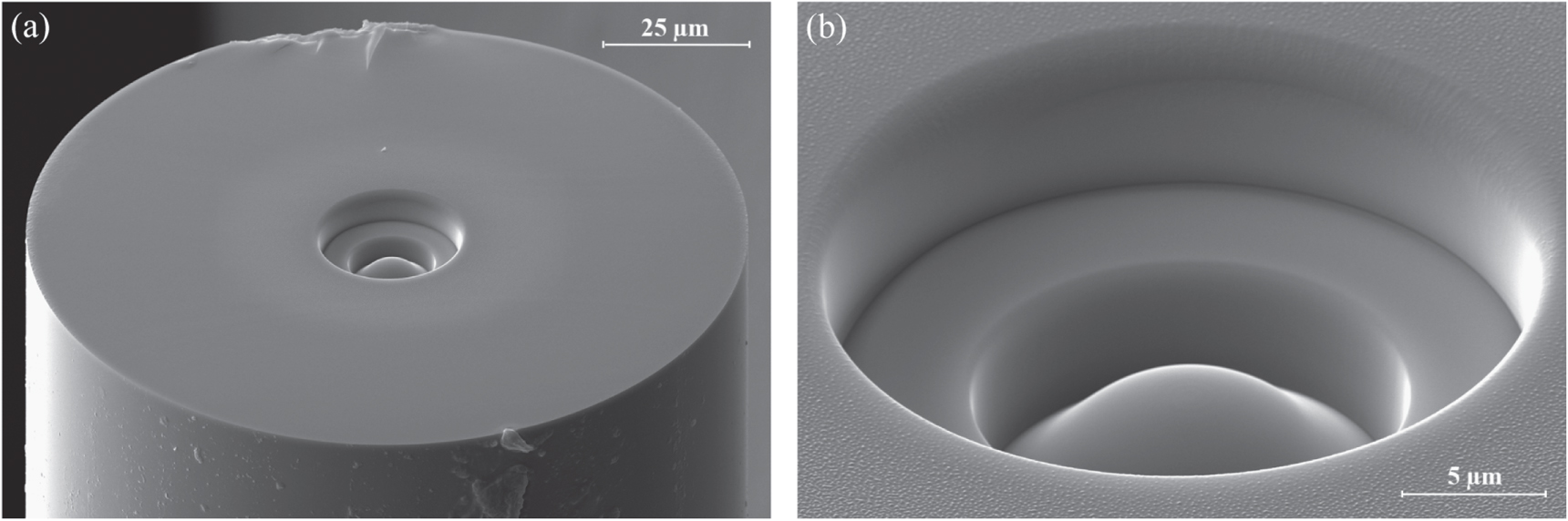
The embedded parabolic lens was fabricated by micromachining an SMF-28e optical fiber using the FIB milling technique carried out using an FEI Helios NanoLab 650 Dual Beam (FIB/SEM) system. The lens was engraved into the cleaved (90° cleave angle) endfacet of the fiber by first milling out a cylindrical section with a diameter of 25 μm and depth of 6.5 μm using 30 keV accelerated  ions with a probe current of 2.5 nA. Subsequently, a grayscale pattern associated with different ion beam exposure dwell times was used to define the parabolic lens into the bottom facet of the cylindrical section, with a diameter of 15 μm and height of 5 μm. The grayscale circular pattern (which determines the dwell time) is minimum at the center and increases radially with a parabolic variation to its maximum value at the edge of the lens. When performing 3D nanofabrication by FIB, redeposition should be taken into consideration [25]. An optimization process (that involved a parametric trial of values) was used to determine the maximum dwell time, volume per dose, and probe current to be 4 μs, 0.15 μm3 nC−1, and 0.23 nA, respectively. These values were found to minimize redeposition and ensure high resolution fabrication of the 3D parabolic lens structure. The typical fabrication time for these parameters is ∼2 h. Reducing the probe current any further would increase the fabrication time without any substantial improvement in the quality of the fabricated lens. It is important to note that the FIB milling depth was controlled through periodic measurements during the milling procedure. SEM images of the fabricated lens are shown in figures 2(a), (b).
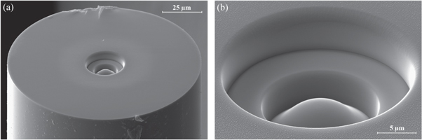
Figure 2. SEM images of a 5 μm-high parabolic lens embedded 6.5 μm below the endfacet of an optical fiber (angled view with a 52° tilt): (a) optical fiber showing the parabolic lens defined in the center; (b) magnified view of the embedded parabolic lens. The fiber facet-lens clearance distance corresponds to the working distance of the parabolic lens.
Download figure:
Standard image High-resolution image3. Numerical simulations and optical characterization
The 3D FDTD method was used to numerically calculate the working distance and spot size as a function of the height of the lens (with a fixed lens diameter of 15 μm). The working distance is herein defined as the distance between the topmost surface of the lens and the location of its maximum intensity along the propagation axis, while the spot size is defined in the beam cross-section as the distance between the positions where the intensity of the Gaussian beam at the working distance drops to 1/e2 of its peak value. The optical properties of an SMF-28e single-mode fiber were used in numerical computations. The refractive index of the fiber core and cladding are taken as nc = 1.4678 and ncl = 1.4625, respectively. The diameter of the core was  . The fundamental mode (linearly polarized) at a wavelength of
  is launched inside the fiber. A non-uniform simulation mesh was used, with 34 mesh cells per wavelength (inside the current material of index n). This corresponds to a resolution around
  . The diameter (D) of the parabolic lens was fixed at
  , which is larger than the supported mode size of the fiber (
 ).
).
The results of the 3D FDTD numerical simulations are shown in figures 3(a), (b). Figure 3(a) shows that, as the lens height varies from 1 to 14 μm, the spot size decays from 5.8 to 1.8 μm. Within the same range of lens heights, the working distance varies from 20 to 1.6 μm, as shown in figure 3(b). Since a spot size of  is optimal for coupling into our input test waveguide (in this work, defined as an inverted taper in silicon, with a cross-section of
  at the edge) [26], we use the curve of figure 3(a) to determine the corresponding lens height of
  (indicated by the red circle in the figure), and then use that lens height to find the adequate working distance of
  , from figure 3(b) (also indicated by the red circle in the figure).
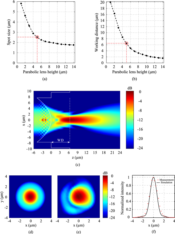
Figure 3. Simulation and characterization results: (a), (b) parabolic lens optical properties (spot size and working distance, respectively), calculated numerically using the 3D FDTD method, as a function of the lens height; (c)–(f) focusing performance of the parabolic lens at 1550 nm—(c) FDTD computed intensity distribution of the beam in the xz plane, (d) FDTD computed intensity distribution of the beam cross-section at the focal plane for the 5 μm-high parabolic lens, (e) measured confocal image, and (f) measured and simulated line profiles along the x axis, with a measured spot size of 2.6 μm.
Download figure:
Standard image High-resolution imageA similar procedure can be used to estimate the working distance and spot size for any other waveguide cross-section requiring a lens spot size different than  . As a result, an embedding depth of
  was selected for the fabricated lens, in accordance with the numerical simulations. The normalized intensity distribution along the xz plane for the selected lens (height of
  ) is shown in figure 3(c). The FDTD calculations return a conversion loss of about
  (between the guided mode inside the optical fiber and the focused beam at the working distance). To validate our results, the simulated beam intensity distribution at the working distance of the designed lens (height of
  ) (see figure 3(d)) was compared with the measured intensity distribution of the fabricated lens (figure 3(e)). The optical characterization was performed through high-resolution confocal measurements at
  , using a high numerical aperture tapered lensed fiber as the scanning probe. The probe has a measured spot size of
  and a working distance of
  . It is worth noting that, from figure 3(f), the spot size of the fabricated lens seems slightly larger than that of the numerical estimate (
 versus
  ). However, this is due to the convolution of the measured intensity profile with the response of the fiber used for the confocal measurement. Upon deconvolution, the spot size of the fabricated lens is estimated to be about
  , which is in good agreement with the numerical prediction. The deconvolution is done assuming that both intensity distributions have a Gaussian-like shape.
4. Fiber-to-waveguide coupling performance
To further evaluate the performance of our embedded structure, we used the fabricated lens to couple light into different test devices (straight waveguide and add-drop microring resonator filter) fabricated on a silicon chip, with the output light collected by a commercial tapered lensed fiber (illustrated in figure 4). The straight waveguide is used to compare the lateral alignment performance between the embedded parabolic lens and the commercial lensed fiber, while the add-drop microring resonator is chosen to demonstrate broadband coupling operation over the whole C-band. The coupling performance (insertion loss, lateral alignment, and longitudinal alignment) of the embedded parabolic lens (with spot size of  ) was benchmarked against a Nanonics lensed fiber (with a measured spot size of
  ), alternating both lenses as input. It is important to note that, during the experiment with both the straight waveguide and the microring resonator add-drop filter, the output fiber was always kept the same (commercial lensed fiber). Light from a tunable laser source (1 mW power) was linearly polarized (transverse electric polarization) using a polarization controller in an edge-coupled optical characterization setup. For coupling into the straight waveguide (figure 4(a)), the longitudinal alignment challenge of the embedded lens is eliminated by directly touching the fiber endfacet on the edge of the photonic chip. On the other hand, the conventional lensed fiber still requires longitudinal alignment in order to assure that we are operating at the right working distance (which maximizes the coupling). In order to analyze the effect of the lateral alignment on the coupling, we conduct cross-section power transmission scans for both input fibers, for a wavelength of
  (center of the C-band).
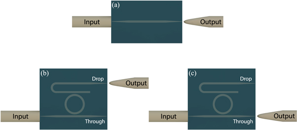
Figure 4. Illustration of the fiber-to-chip coupling experiments: (a) photonic chip consisting of a straight test waveguide; (b), (c) photonic chip consisting of an add-drop microring resonator filter, when the output fiber is at the drop port and through port, respectively. During the experiments, the input fiber is switched between the fabricated embedded lens and the commercial lensed fiber, while the output fiber is always kept the same (commercial lensed fiber).
Download figure:
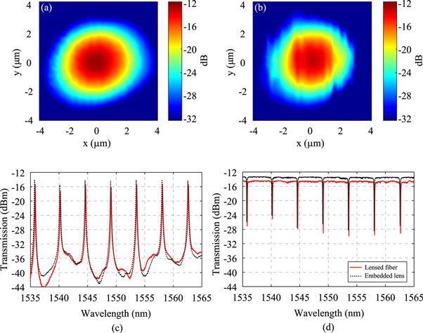
Standard image High-resolution imageThe cross-section power transmission scans (with the straight test waveguide) for both lenses are shown in figures 5(a), (b). For obtaining the results shown in figures 5(a), (b), the respective input lens is placed on a three-axis piezo-controlled stage. The lens was then moved in the lateral direction with increments  . Results show that the lateral alignment effect on the coupling performance for the embedded parabolic lens is comparable (
 higher power transmission) to that of the commercial lensed fiber. It is worth nothing that the lateral alignment of the embedded fiber is always performed before bringing it in physical contact with the edge of the photonic chip. In the particular case of the results of figure 5(a), the lateral scan is performed at a small distance away from the edge, in order to prevent damaging the chip.
Figure 5. Fiber-to-chip coupling performance evaluation: (a), (b) power transmission lateral scan for coupling into the straight waveguide at 1550 nm, when the input is (a) the embedded parabolic lens, and (b) the commercial lensed fiber; (c), (d) power transmission in the C-band of the add-drop microring resonator filter (with both input lenses) for the drop and through ports, respectively.
Download figure:
Standard image High-resolution image
In the setup with the microring resonator add-drop filter (figures 4(b), (c)), we look at the transmission spectra at both the drop and through ports (figures 5(c), (d), respectively), for wavelengths in the C-band. Once again, the longitudinal alignment of the embedded parabolic lens is completely eliminated by touching the fiber endfacet to the edge of the photonic chip, while the commercial lensed fiber longitudinal alignment is still needed in order to maximize the coupling. In both cases, the lateral alignment is still required. It is important to note that the lateral tolerance for both lenses is similar, as both lenses produce output beams with similar spot sizes. While the insertion loss and lateral alignment requirements for both lenses are comparable, the significant advantage of the embedded parabolic lens is the intrinsic longitudinal alignment. From the results, the coupling performance of the embedded lens was about 1–1.5 dB higher than the commercial lensed fiber (which we still consider comparable). In both experiments (straight waveguide and microring), the slightly lower coupling of the latter lens can be attributed to a combination of factors: (i) small experimental longitudinal misalignment, (ii) slightly different spot size, and (iii) non-uniformity of the lens surface. Nevertheless, these results show that, by completely eliminating the longitudinal alignment, we can achieve comparable coupling performance with the fabricated embedded lens. The by default longitudinal alignment of the embedded structure largely simplifies any required packaging procedure. It is worth noting that this longitudinal alignment also ensures (i) a more precise axial angular alignment, (ii) an additional protection against the accumulation of micro-particles and possible contaminants present in the air, and (iii) mechanical protection of both the lens and the endfacet of the waveguides on the photonic chip. Although the FIB fabrication process is repeatable with high accuracy, small dimensional variations in the embedded clearance height and/or in the parabolic lens height may still result in a small coupling loss.
5. Conclusions
This study presents a compact design for fiber-to-waveguide coupling with a parabolic lens engraved beneath the endfacet of an SMF-28e single-mode fiber. The FIB milling technique was used for the fabrication process, which structurally positioned the tip of the lens at a distance from the endfacet precisely corresponding to its working distance. FDTD numerical simulations were used to determine the optimal lens dimensions for a specific desired spot size and corresponding working distance. Optical characterization of the fabricated lens showed that the embedded design is comparable to the commercial lensed fiber in terms of coupling performance (insertion loss and lateral alignment). However, the longitudinal alignment procedure is eliminated for the embedded lens, since the facet-lens clearance distance is equal to the working distance of the lens. In addition, the angular alignment is facilitated, and the embedded lens structure offers additional mechanical and environmental protection for the lens and chip endfacets. The proposed embedded lens, in conjunction with traditional v-grooves, would allow a complete passive plug-and-play alignment packaging solution.
Acknowledgments
The authors thank Ayoola Brimmo for useful discussions and comments on the manuscript.