

Abstract
Attempts to improve the efficiency of kesterite solar cells by changing the intrinsic stoichiometry have not helped to boost the device efficiency beyond the current record of 12.6%. In this light, the addition of extrinsic elements to the Cu2ZnSn(S,Se)4 matrix in various quantities has emerged as a popular topic aiming to ameliorate electronic properties of the solar cell absorbers. This article reviews extrinsic doping and alloying concepts for kesterite absorbers with the focus on those that do not alter the parent zinc-blende derived kesterite structure. The latest state-of-the-art of possible extrinsic elements is presented in the order of groups of the periodic table. The highest reported solar cell efficiencies for each extrinsic dopant are tabulated at the end. Several dopants like alkali elements and substitutional alloying with Ag, Cd or Ge have been shown to improve the device performance of kesterite solar cells as compared to the nominally undoped references, although it is often difficult to differentiate between pure electronic effects and other possible influences such as changes in the crystallization path, deviations in matrix composition and presence of alkali dopants coming from the substrates. The review is concluded with a suggestion to intensify efforts for identifying intrinsic defects that negatively affect electronic properties of the kesterite absorbers, and, if identified, to test extrinsic strategies that may compensate these defects. Characterization techniques must be developed and widely used to reliably access semiconductor absorber metrics such as the quasi-Fermi level splitting, defect concentration and their energetic position, and carrier lifetime in order to assist in search for effective doping/alloying strategies.
Export citation and abstract BibTeX RIS

Original content from this work may be used under the terms of the Creative Commons Attribution 3.0 licence. Any further distribution of this work must maintain attribution to the author(s) and the title of the work, journal citation and DOI.
1. Introduction
Kesterite materials—Cu2ZnSnS4 (CZTS), Cu2ZnSnSe4 (CZTSe), Cu2ZnSn(S,Se)4 (CZTSSe) are multinary compounds that can be synthesized in different off-stoichiometric compositions and therefore offer rich possibilities for defect engineering. According to the compositional classification of Lafond et al [1] that was further extended by Gurieva et al [2], up to 12 compositional-type materials can be distinguished, each of them corresponding to different cationic distribution giving rise to most probable secondary phases and intrinsic point defects. The highest efficiency solar cells are obtained, regardless of the kesterite absorber synthesis method, for Cu-poor, Sn-stoichiometric and Zn-rich compositions located around the so-called 'A' compositional line. The record 12.6%-efficient [3] (or 12.7% by improving emitter [4]) CZTSSe solar cell demonstrated by the IBM group in 2014 had a targeted cation composition of Cu/(Zn + Sn) = 0.8 and Zn/Sn = 1.1 and did not include any intentional doping, although the presence of small quantities of alkali elements stemming from the soda-lime glass (SLG) substrate could not be excluded.
From the numerous combinatorial studies performed since the pioneering report of Katagiri in 2005 [5], it became clear that just by changing the absorber stoichiometry it was not possible to further advance the device performance. Thus, addition of extrinsic elements to the kesterite matrix in various quantities has emerged as a popular topic aiming to ameliorate electronic properties of the kesterite absorbers. This trend has also been inspired by the related CIGS and CdTe technologies, where the use of extrinsic species to passivate intrinsic defects and provide shallow dopants was combined with the bandgap engineering through substitutional doping (alloying) to boost the solar cell efficiencies beyond 22%.
This article aims to review extrinsic doping and alloying concepts for the kesterite absorbers, although in most (all) cases, a combination of the intrinsic and extrinsic defects will determine the final absorber properties. The review is limited to the extrinsic elements that do not alter the parent zinc-blende derived crystal structure of kesterites where all atoms have tetrahedral coordination.
1.1. Intrinsic doping
Before reviewing extrinsic elements, it is necessary to recall electronic properties of the non-intentionally doped kesterites, which have been summarized in several reviews [6, 7]. For the samples without secondary phases, numerous native lattice defects exist including Cu, Zn, Sn or S(Se) vacancies, (VCu , VZn , VSn and VS or VSe), interstitials (Cui, Zni, Sni and S(Se)i), as well as antisites (CuZn, ZnCu , ZnSn , SnZn , etc). Besides these, the donor and acceptor defects may also compensate and attract each other, forming defect clusters (VCu + ZnCu, 2CuZn + SnZn, ZnSn + 2ZnCu).
CZTS, CZTSe and CZTSSe samples have been widely found to show the p-type (hole mediated) conductivity intrinsically, while n-type samples have not been reported. The p-type conductivity is attributed to a high population of shallow acceptor-like defects such as Cu vacancies (VCu) and CuZn antisites, whose density depends on the Cu/(Zn + Sn) and Zn/Sn ratio. Despite the certainty of the p-type character, the reported hole concentrations from different experiments vary significantly, spanning a range from 1.2 × 10¹⁵ to 3.1 ×1020 cm−3 [6]. Three factors may contribute to the significant variation in the carrier concentration numbers including the presence of secondary phases (e.g. Cu2(S,Se) or Zn(S,Se)), deviations in the cationic ratios of Cu/(Zn + Sn) and Zn/Sn, uncertainties of different measurement techniques and often unintended doping by elements such as Na from the glass substrate.
The doping concentration is typically deduced from capacitance–voltage (C–V) measurements of complete solar cell devices, where the acceptor concentration NA can be calculated from the Mott–Schottky plots assuming an n+p-type heterojunction. The obtained NA values, however, can be affected by several non-idealities such as an inhomogeneous doping profile and contributions from deep defects [8, 9]. The C–V sweep of the 12.6% device resulted in the concentration NA ∼ 2 × 1016 cm–3 at zero bias [3]. The drive level capacitance profiling (DLCP) of the same sample, which should be sensitive only to bulk defects, yielded somewhat lower drive level densities of < 7 × 1015 cm−3. Similar values have been frequently reported and can be used as reference points when reviewing the doping densities induced by extrinsic dopants in the following sections.
Another important semiconductor metric is the minority carrier lifetime that influences the carrier diffusion length and eventually limits the solar cell efficiency. Time-resolved photoluminescence (TRPL) is frequently employed to compare different kesterite absorbers whereby the measured PL decay time on the order of 1...10 ns is often associated with the minority carrier lifetime of the material. However, the reported lifetime values should be treated with precautions. It has been analyzed by Hages et al [10] that the PL decay times in kesterite materials are strongly influenced by minority carrier trapping, surface effects and energetic relaxation, and therefore do not correspond to the effective minority carrier lifetimes. With this in mind, the present article does not contain detailed discussions on reported PL time decays but suggests a need to develop more precise techniques for accessing minority carrier lifetime.
1.2. Extrinsic elements in this review
Figure 1 illustrates the extrinsic elements covered in this review. Depending on the concentration of the impurity element in the kesterite matrix, two cases can be distinguished: doping and alloying. These namings are not strict scientific terms (e.g. 'alloying' is often reserved for metallic alloys only whereas doping usually refers to a change in charge carrier density or type by introducing acceptor or donor states) but both terms have been widely adopted by the kesterite community. The doping elements are marked in blue, and the elements that can form substitutional alloying are shown in orange. For some elements, e.g. Li or Ge, both doping and alloying are considered.

Figure 1. Doping and alloying elements covered in this article.
Download figure:
Standard image High-resolution imageThe purpose of doping is to change electronic, electrical, charge transport and interface properties without changing the crystal structure and altering the optical properties of the host material. In contrary, alloying is referred to an isoelectronic cation substitution to introduce ionic size mismatch, which can be particularly interesting for band engineering of the absorber. In this article, the term alloying is used if the concentration of extrinsic element can exceed 1 mol. % without changing the parent kesterite structure. Both doping and alloying effect can also be combined. For instance, both doping and alloying strategies have been crucial to reach very high efficiencies in CIGS cells, with the use of alkali elements for doping and alloying with Ga for band grading [11].
Extrinsic dopants can be divided into isoelectronic (i.e. with oxidation states matching to the replaced matrix element) and non-isoelectronic ones (e.g. Group III elements). There have been also other elements reported to replace Zn for Be, Ca [12, 13], Sr [14] or Ba [15, 16] and Sn for Ti, Zr, or Hf [17], but these will not be covered in this review as some of them, e.g. Ba, lead to the change of the kesterite crystal structure. When comparing ionic radii of the matrix and doping elements, crystal (ionic) radii for the tetrahedral coordination are taken from Shannon's tables [18], also other radii scales can also be used.
2. Group I elements
2.1. Hydrogen (H)
Hydrogen has been widely accepted as an effective passivation element for Si. In recent advanced hydrogenation technology, the photon-modulated charge state of hydrogen leads together with the heat treatment to an effective passivation of defects [19]. Similar to Si, in most semiconductors (e.g. GaAs, GAP, InP, and ZnSe) hydrogen impurities, being an amphoteric center, do not produce free carriers, yet hydrogen does dope chalcopyrite [20]. Hydrogen has been experimentally demonstrated to cause p-to-n conductivity-type conversion in CuInSe2 through ion implantation [21]. This was further confirmed by first principle calculations [20] shown in figure 2. The calculations show that the effect of hydrogen in nonstoichiometric chalcopyrite (containing VCu and/or IIICu + 2VCu) depends on the interplay between passivation of acceptor-like defects (i.e. (VCu + H)0, hydrogen resides next to copper vacancy) and n-type doping (i.e. pairing of H+ with (IIICu + 2VCu)0).

Figure 2. The LDA-corrected formation energies of Hi, HCu, (VCu + H), and (InCu + 2VCu + H) in CuInSe2 as a function of the Fermi energy EF for Cu-poor, In-rich, and Se-rich conditions. Two different hydrogen sources are considered: atomic H (left scale) or molecular H2 (right scale). The zero of EF is set to the valence-band maximum. +, 0, −denote the charge states. The transition energies are marked by filled circles. Reprinted with permission from [20]. Reprinted (figure) with permission from [20], Copyright (2003) American Physical Society.
Download figure:
Standard image High-resolution imageRecently, Hao et al reported the potential passivation role of hydrogen in pure sulfide kesterite [22]. Hydrogen was introduced into the surface region of kesterite through the atomic layer deposition (ALD) of Al2O3 on kesterite (see figure 3). Though no Al was detected by XPS, the open circuit voltage (VOC) of completed kesterite devices was improved by about 70 mV. Additionally, their Kelvin probe force microscopy (KPFM) measurements revealed the passivation effect from hydrogen, where the contact potential difference of kesterite with incorporated hydrogen from ALD had a significantly different profile from that of the reference. The ALD Al2O3-treated samples exhibited a much smoother contact potential difference (CPD) profile (less CPD variation between grain boundary and grain interior) and much narrower CPD distribution than the kesterite reference. It was speculated that the hydrogen atom could bond with sulfur anions having dangling bonds at the grain boundaries. To clarify the effect of hydrogen in terms of its location in the kesterite lattice, detailed first principle calculations are required.

Figure 3. (a) Elastic Recoil Detection Analysis (ERDA) of the CZTS device with 0, 3 and 5 cycles of ALD-Al2O3, (b) Open circuit voltage of the CZTS devices with different cycles of ALD-Al2O3 on absorber layer. (c) Contact potential difference distribution of kesterite reference, reference + NH4OH etching, and kesterite-3cycles of ALD-Al2O3 + NH4OH etching. Reprinted with permission from [22]. (2018) John Wiley & Sons. (© 2018 WILEY‐VCH Verlag GmbH & Co. KGaA, Weinheim).
Download figure:
Standard image High-resolution image2.2. Lithium (Li)
The ionic radius of Li+ (0.73 Å) is very close to that of Cu+ (0.74 Å), and thus has the highest probability to be incorporated into the lattice of kesterite phase and affect the photovoltaic properties compared to heavier alkali elements. Surprisingly, the studies on Li doping/alloying on CZTS are quite recent. In 2015, Xin et al [23] first reported Li doping in dimethyl sulfoxide (DMSO) precursor solution processed CZTSSe absorber by adding the Li salts directly into the solution. A dramatic change in the electronic property of the CZTSSe upon Li doping was found although the Li concentration in the final film was very low (Li/Cu = 3.9 × 10⁻⁵). The conductivity of the doped film was improved by one order of magnitude and the electrical potential at grain boundaries was reversal to the non-doped one (figure 4) which results in an upward band bending and reduces recombination by repelling minority carriers from the detrimental defect rich grain boundaries. The performance of CZTSSe solar cells was improved by more than 30% to an active-area efficiency of 11.8%.
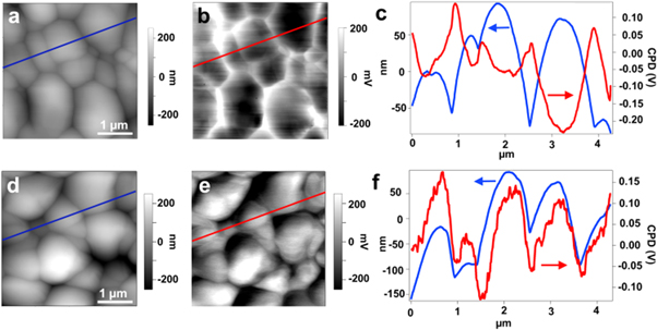
Figure 4. AFM topography images (a), (d), Scanning Kevin probe microscopy (SKPM) potential maps (b), (e) and. plots of the topography and potential linescans (c), (f) (a)–(c) of CZTSSe films without (a)–(c) and with Li-doping (d)–(f). Reproduced from [23] with permission of The Royal Society of Chemistry.
Download figure:
Standard image High-resolution imageYang et al [24] demonstrated that Li incorporates into the lattice of CZTSSe and tunes the band gap of LixCu2−xZnSn(S,Se)4 without significant effect on carrier concentration and crystal growth [25] when films were selenized on quartz substrates. Later, they reported [26] that only traces of Li (Li/Cu = 3.4 × 10⁻⁴) were left in the final CZTSSe film when the films were fabricated on SLG substrates. A Li/Na exchange mechanism was proposed for the observed phenomenon. The Li alloying and band gap tuning are also achieved by Lafond et al [25] from a ceramic synthesis route. Cabas-Vidani et al [27] confirmed the lithium alloying in the kesterite thin films (LixCu1−x)2ZnSn(S,Se)4 in the range x = 0 to 0.12 as measured by inductively coupled plasma mass spectrometry (ICP-MS), and a widening of the bandgap from 1.05 to 1.18 eV was observed. Morphology improvement and apparent carrier concentration increase from 3 × 1015 cm−3 to 5 × 1016 cm−3 was observed when increasing x from 0 up to 0.07, and a corresponding device had an active area efficiency of 12.2%. In a comprehensive study on the effects of all alkali elements in CZTSSe, Haass et al [28] found that Li is the most favorable among all alkalis, it improves the crystallization and it requires a comparatively high Sn/(Cu + Zn + Sn) content for the maximum device efficiency. The apparent carrier concentration estimated from C-V measurements varied in a broad range 1015...1018 cm−3 when changing (decreasing) the Sn content yet keeping the same Li content, indicating that the intrinsic doping rather prevails. A champion device with 11.5% efficiency (12.3% active area) was achieved using a 'high' Li concentration of 0.75 at% at an optimized Sn content.
Although the results and the explanation on the effect of Li doping/alloying differ and even contrast to each other, partially due to variation in material preparation conditions and matrix composition, some conclusions can be drawn based on the available reports [23–32]: (1) Li alloys with CZTS and widens the band gap of (LixCu1−x)2ZnSn(S,Se)4 [24, 25, 27]; (2) incorporation of Li to kesterite is sensitive to Na so that Li alloying is more easily achieved without Na, in the ceramic route [25] or on quartz substrate, or using a blocking layer to prevent Na diffusion from SLG [24, 27]. The presence of Na diffused from SLG greatly reduces the Li doping concentration [23, 26]; (3) Li doping/alloying improves photovoltaic performance regardless the doping concentration, however, the mechanism on how Li doping/alloying improves device performance remains unclear.
2.3. Sodium (Na)
Since the early 1990's, it is known that Na leads to significant improvements on CIGS solar cells [33]. For kesterite solar cells, the effects of Na were thoroughly investigated [34–37] and it has been shown that Na diffusion from SLG has similar positive effects on absorber morphology and device properties in kesterite devices [37, 38]. Na treatment increases grain size and improves the overall absorber layer morphology, increases doping concentration and was shown to yield improved opto-electronic properties of the absorber layer. The increased grain size is attributed to the capability of Na to form low-temperature Na2Sex liquid phases [37] that act as a fluxing agent and facilitate grain growth. The improvements of opto-electronic properties are associated with the passivation of defects at grain boundaries and interfaces, which are the predominant locations for Na inside the absorber layer [30]. Atom probe tomography (APT) measurements revealed that the sodium concentration in the grain interior is only about 20% of what is measured by ICP-MS in the absorber layer, which supports the assumption that sodium is primarily segregated at the grain boundaries and absorber surface [39].
NaCl treatment of solution-processed kesterite solar cells was investigated by Sutter-Fella and Werner [37, 40], who showed that a tailored addition of Na improves grain growth and optoelectronic properties, especially open-circuit voltage VOC and fill-factor FF. However, only a fraction of the added sodium is eventually incorporated into the processed absorber layer, e.g. adding nominally 3.33 at% NaCl resulted in only 0.18 at% in the processed absorber layer as determined by ICP-MS measurements [28]. An 11.2%-efficient CZTSSe solar cell is fabricated using NaCl treatment (figure 5) and the device features a VOC - deficit (defined as Eg/e − VOC) of only 0.57 V, which is amongst the lowest for kesterite solar cells [41]. The reduced VOC - deficit is attributed to a low diode saturation current and ideality factor, which are signatures of the semiconductor material with a low concentration of recombination centers. Even a higher efficiency of 11.6% was obtained for a Na-doped CZTSe absorber grown by thermal co-evaporation [42], proving the effectiveness of the Na doping.
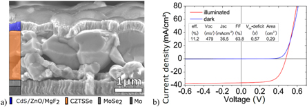
Figure 5. (a) SEM cross section exhibiting large grained morphology and (b) dark and illuminated current density-voltage (J-V) measurement of the 11.2% efficient solution processed kesterite solar cell treated with NaCl. Reprinted with permission from [41]. John Wiley & Sons. (© 2015 WILEY-VCH Verlag GmbH & Co. KGaA, Weinheim).
Download figure:
Standard image High-resolution image2.4. Potassium (K)
Based on its chemistry, K could be located on the Cu positions within the kesterite lattice, however, previous studies about the localization of potassium in chalcogenide absorber layers by APT revealed that potassium is segregating at the grain boundaries [43, 44]. Due to the large size of 1.51 Å of the K + ion and thus a high substitution energy of 1.53 eV, alloying of potassium within the kesterite lattice is unlikely [30]. Potassium addition can enhance the (112) preferred orientation and reduce ZnS secondary phases in solution-processed CZTS absorber layers [45]. For solar cell devices, a reduction in the series resistance was observed upon potassium addition [45] whereas the carrier concentration could be increased for potassium as compared to untreated samples [32, 46]. Potassium is a potent agent to promote grain growth during the absorber layer synthesis.
Potassium treatment of kesterite solar cells can be conducted using two main approaches: the potassium-fluoride post deposition treatment (KF-PDT) [47] and the bulk treatment [48]. KF-PDT of solution-processed kesterite solar cells with various KF thicknesses exhibits a decrease in short-circuit current density JSC, FF and efficiency with increasing KF thickness, which originates from a severe blocking of the photocurrent (figure 6(a)). The CdS buffer layer growth is not affected by KF-PDT, but the buffer layer exhibits a photoconductivity effect in external quantum efficiency (EQE) measurements. Although KF-PDT improves the VOC, it is evident that the surface chemistry does not yield a beneficial interface layer and thus, no performance improvements can be observed [47].

Figure 6. (a) J-V curves of KF-PDT treated solution processed kesterite solar cells that exhibit increased blocking of the JSC with thicker KF layer (0 nm–60 nm). Reprinted from [47], Copyright (2017), with permission from Elsevier. (b) Increase of the apparent carrier concentration as determined by C-V measurements on bulk treated solution processed kesterite solar cells. Copyright © 2018, Author(s). Reproduced from [48]. CC BY 4.0.
Download figure:
Standard image High-resolution imageThe K bulk treatment of kesterite solar cells leads to an enhanced grain growth and improved photovoltaic (PV) properties resulting in devices close to 10% conversion efficiency. K is an effective fluxing agent and additionally suppresses incorporation of Na from the soda lime glass. Incorporation of high concentrations of K also reduces the loss of Sn, which results in a change of order/disorder of the Cu/Zn sub-lattice and thereby additionally widens the bandgap and increases the tetragonal distortion [48]. Potassium doping increases the carrier concentration as derived from C-V measurements shown in figure 6(b). Higher nominal K concentrations require an adjustment of the Sn content in the absorber layer in order to avoid formation of Sn(S,Se)2 secondary phase and thus deterioration of the device performance.
2.5. Rubidium (Rb) & caesium (Cs)
Rubidium and caesium are alkali elements with ionic radii of 1.66 Å and 1.81 Å, respectively, which is significantly larger than Cu with 0.74 Å. XRD measurements on Rb and Cs treated CZTSSe absorber layers indicated that Rb and even more so Cs are not replacing CZTSSe atoms in the kesterite lattice [32]. The impact of Rb and Cs on kesterite absorbers and respective device performance was studied several times [28, 29, 32]. Equivalent to the lighter alkali metals, Rb and Cs can form alkali poly-selenide liquid phases at comparably low temperatures. These liquid phases act as a fluxing agent during the selenization process and improve grain size and the overall absorber layer morphology. However, a too high concentration leads to the fragmentation of the absorber layer and a dense but small-grained morphology with a high density of grain boundaries (figure 7). Rb and Cs treated samples exhibit a large-grain morphology for 'low' nominal alkali concentration, whereas a 'high' alkali content results in a small-grain morphology. The final device efficiencies are correlated with the absorber layer morphology, and the highest efficiency of 8.8 and 9.1% were obtained for Rb and Cs, respectively, for 'low' concentration of ca. 0.15 at% (relative to all elements, as measured by ICP-MS) [28]. It is not clear how much of Rb and Cs are located inside the kesterite grains so it is assumed that most of them reside at grain boundaries.
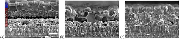
Figure 7. SEM cross sections of full devices including a window layer with no alkali treatment, (a) Rb treatment for 'low' and (b) 'high' alkali concentrations. © 2017 The Authors. Published by WILEY‐VCH Verlag GmbH & Co. KGaA, Weinheim. Reproduced from [28]. CC BY 4.0.
Download figure:
Standard image High-resolution image2.6. Comparison of alkali elements
Several studies comparing different alkali elements and their effects on kesterite properties and device performance have been published [29, 31, 32, 49]. However, no consistent experimental results have been obtained concerning the impact of alkali treatments on the device properties and performance. A study by Haass et al [28] revealed that each alkali element requires a different absorber composition to achieve the highest PV performance (figure 8(a)). From Li to Cs the nominal Sn concentration (Sn/Cu + Zn + Sn) required for best device performance should be reduced by more than 20% (relative).
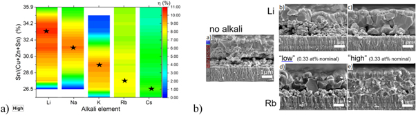
Figure 8. (a) Device efficiency as a function of the nominal Sn content and the alkali elements. The color code resembles the efficiency up to 11% and the stars indicate the Sn content yielding highest efficiency for a given alkali element. (b) SEM cross sections of the full devices visualize the impact of no alkali, Li and Rb (both 'low' and 'high' concentration) treatment on the absorber layer morphology. © 2017 The Authors. Published by WILEY‐VCH Verlag GmbH & Co. KGaA, Weinheim. Reproduced from [28]. CC BY 4.0.
Download figure:
Standard image High-resolution imageThe alkali concentration yielding the best devices for Li (11.1% efficiency), Na (10.0%) and K (10.0%) is 10 times higher compared to optimum alkali concentration for Rb (8.8%) and Cs (9.1%). ICP-MS measurements show that the alkali content in the kesterite layer is proportional to the nominal input, however, light dopants like Li tend to be lost during the processing steps (in the case of spin-coated precursor solutions). As the alkali elements are preferably located along the grain boundaries [50, 51], the overall amount measured by ICP-MS, which does not discriminate between alkali elements inside grains or at the grain boundaries, is expected to be higher for samples with a higher density of grain boundaries.
The morphology for each alkali element and concentration indicates that the lighter alkali elements require a higher concentration to reach a similar improvement in morphology as compared to the heavier alkali elements. This could be due to lower melting points for alkali-poly-selenide phases of heavier alkali species as compared to lighter ones [52–56]. Because of the lower melting points the heavier alkali elements act more efficiently as a fluxing agent and, hence, lower concentrations are required to achieve similar grain size improvements.
The PV parameters correlate with the changes in morphology with best devices exhibiting large grains throughout the whole absorber layer with a low density of grain boundaries (figure 8(b)). The formation of Sn(S,Se)2 secondary phase is increased for the heavier alkali elements and for 'high' concentrations. As revealed by EQE and C-V measurements the apparent carrier concentration varies by three orders of magnitude depending on the Sn content, except for high Rb and Cs content where a constant kesterite composition and therefore constant apparent carrier concentration is observed. A ranking of best device performances employing alkali treatment resulted in the order of Li > Na > K > Rb > Cs based on the statistics of more than 700 individual cells.
TRPL measurements of numerous alkali-containing devices yielded PL decay times in the range 1...8 ns but no correlation between PL decay time and efficiency, or decay time and alkali ionic radii could be detected [57]. That is in line with the observations of Hages et al [10], who conclude that the minority carrier trapping can severely alter (extend) measured PL transient times.
2.7. Silver (Ag)
One of the most explored methods to improve the efficiency of CZTS solar cell is partial substitution of Cu by Ag. The increase in VOC on both CZTS or CZTSe is evident in most of the reported studies [58–62]. This strategy was theoretically proposed as an effective method to reduce the concentration of CuZn antisite pairs [63, 64]. The substantially higher crystal radius of Ag+ (1.14 Å) compared to Cu+ (0.74 Å) contributes to the higher formation energy of antisite defects and Ag-related defect complexes such as AgZn + ZnAg and 2AgSn + SnZn in Ag2ZnSnS4 (AZTS) based on theoretical calculations [18, 65–67] (figure 9(a)). The lower valence band edge in AZTS (by 0.74 eV) also plays an important role in decreasing the amount of antisite defects [65]. However, it also increases the formation energy of the other acceptor defects which makes the intrinsically n-type AZTS difficult to be doped p-type. Besides the higher formation energy, the Ag- and Zn- related defects form shallow defects and consequently their defect cluster creates smaller band edge shifting compared to CZTS (see figure 9(b)). In the case of partial Ag substitution, low level (<6% Ag) Ag substitution is expected to suppress Cu-Zn disorder only under Cu-rich and constrained Cu-poor conditions (presence of ZnS, SnS, and Cu-deficient phases with Zn- and Sn-rich condition); meanwhile, at a high level (>6% Ag) Ag substitution, the disorder suppression is more effective because higher formation energy of antisite defects [68].

Figure 9. (a) The calculated formation energy change as a function of the elemental chemical potentials (growth conditions) for low-energy defects and defect complexes in Ag2ZnSnS4; (b) the band edge shift caused by the low-energy defect complexes. The GGA/DFT gap is corrected to the experimental value of 2.01 eV. The band edge shift is calculated assuming one defect complex in a 64-atom supercell. Reprinted with permission from [65]. John Wiley & Sons. (© 2016 WILEY‐VCH Verlag GmbH & Co. KGaA, Weinheim).
Download figure:
Standard image High-resolution imageThere are several experimental studies for (Cu,Ag)2ZnSn(S,Se)4 (CAZTSSe). (Cu1-xAgx)2ZnSnS4 (CAZTS) and (Cu1-xAgx)2ZnSnSe4 (CAZTSe) crystal powders with 0 ≤ x ≤ 1.0 have been reported to have tetragonal kesterite structure based on Rietveld refinement analysis of XRD and bandgap from 1.5 to 2.01 eV for CAZTS and from 1.0 to 1.34 eV for CAZTSe [69]. Recently, another study using neutron and x-ray diffraction suggests that CAZTSe with x = 0.17 and 0.46 crystallize in the stannite type structure and thus suppress Cu/Zn disorder while the end members of the solid solution are reported to crystallize in the kesterite structure [70]. In terms of optoelectronic properties, Gershon et al reported reduction in band tailing from CZTSe to AZTSe based on the reduction of the band tailing parameter (γ) extracted from EQE with a value of ≈18 meV which is half of the one for CZTSe (≈33 meV) [71]. In addition, there is a change of majority carriers from p-type (for CZTSe) to n-type (for AZTSe) which is accompanied by a significant decrease in carrier concentration and increase in Hall mobility (see figure 10). They also first demonstrated a reduction in the VOC deficit (Eg/e − VOC) from about 660 to 580 mV and device performance improvement from 9% to 10.2% efficiency for the 10% Ag substituted CZTSe using a co-evaporation process [58]. Similar results for CAZTSe is also obtained through nanoparticle ink synthesis which achieved device improvement up to 7.2% for CAZTSe at 5% Ag substitution due to improved grain growth, improved minority carrier lifetime, reduced defect formation, and reduced potential fluctuations [60].

Figure 10. (a) Carrier density and (b) majority carrier mobility as a function of Ag/(Ag + Cu) in CAZTSe. Reprinted with permission from [58]. John Wiley & Sons. (© 2016 WILEY‐VCH Verlag GmbH & Co. KGaA, Weinheim).
Download figure:
Standard image High-resolution imageFor sulfur-based CAZTS, Wong et al reported the first solar cell device improvement from 4.9% to 7.2% based on molecular method using metal salts precursor [59]. The power conversion efficiency for pure sulfide kesterite with Ag substitution was further improved to 8.3%, with the suppression of non-radiative defects as the main reason for this improvement [72]. The incorporation of Ag (<7 mol% of Ag/(Ag + Cu)) improved the grain size, increased the depletion width, decreased the charge carrier density, and improved the PL decay time from 1.9 ns for non-intentionally doped CZTS to 3.6 ns for 5 mol% Ag-doped [59, 72].
Similar results are also obtained for CAZTS (Ag/(Ag + Cu) of ca. 0.02) deposited by spray pyrolysis, where the use of an Ag-incorporated film improved the band alignment at the CdS–CZTS interface [73]. In that case the conduction band-offset at the absorber-buffer interface estimated from x-ray photoelectron spectroscopy and EQE measurements was reduced from −0.25 eV for the CdS-CZTS down to -0.17 eV for the CdS-CAZTS heterointerface [73].
Following these positive results, several synthesis strategies were explored to improve the Ag-substituted CZTSSe. Qi et al obtained the highest solar cell efficiency of 10.36% for CAZTSSe at 3% Ag substitution using a solution-based method [57]. They observed a reduction of the VOC deficit from 727 mV (CZTSSe without Ag) to 601 mV (CAZTSe with 3 mol% Ag).
Another strategy of using Ag is by engineering the interface band bending and defect elimination, by placing a higher Ag content CAZTSSe at the back and front interface to create V-shape Ag-graded film [7, 62, 65]. The highest efficiency of 11.2% with a 110 mV VOC enhancement was achieved due to the improvement of the distance between Fermi levels and conduction bands and decrease in CuZn defects at the interface [61]. The energetic difference between the Fermi level and conduction band of the Ag-graded CdS/CAZTSSe heterojunction was estimated from ultraviolet photoelectron spectroscopy and PL measurements to be 100 mV smaller than that of the CdS/CZTSSe heterojunction [61]. To conclude, Ag substitution has shown encouraging results in tackling VOC limitation in CZTS solar cell based on the experimental evidence of reduced band tailing parameter (γ), improved photoluminescence decay time, and better band level alignment at the interface.
3. Group II elements
3.1. Magnesium (Mg)
It was suggested that the substitution of Cu or Zn by other elements such as Mg could suppress the antisite defects CuZn and/or ZnCu formation that limit kesterite solar cells performance [13]. Several studies about the Mg incorporation into kesterite have been published, but the observed effects of Mg are contradictory. For instance, Cu2MgSnS4 thin films grown by ultrasonic co-spray pyrolysis showed p-type conductivity and band-gap energy of 1.76 eV [74]. In contrary, n-type conductivity was estimated for (Cu2-xMgx)ZnSnSe4 bulk materials with x = 0.1–0.4, which was attributed to the formation of the donor-type MgCu antisite defects [75]. The formation of stable Cu2MgSn(S,Se)4 was calculated based on the density functional theory [13], whereas a complete phase separation was predicted by [64].
Regarding solar cells with Mg incorporation, Cu2Zn1-xMgxSn(S,Se)4 absorber layers with variable Mg concentration x = 0...1 were deposited using the solution approach [76]. For heavy Mg alloying with x = 0.55...1 the phase separation of Cu2SnSe3, MgSe2, MgSe and SnSe2 occurs in agreement with literature predictions [64], whereas a lower Mg concentration of x = 0.04 resulted in the kesterite phase. An apparent carrier concentration of 1 × 1016 cm−3 was measured for Mg-doped kesterite solar cell device, confirming the p-type conductivity. Raman spectroscopy indicated that structural defects can be reduced in Mg-containing absorbers as compared to the dopant-free reference samples, resulting in the highest device efficiency of 7.2% for a Mg-doped cell measured in [76].
3.2. Cadmium (Cd)
Cd alloying of kesterite (CZCTS) was proposed to reduce the impact of CuZn and ZnCu antisite defects. The formation of large population of CuZn and ZnCu antisite defects is mainly due to the close cation sizes and chemical electronic properties of Cu+ and Zn2+ in kesterite system [77]. Cd is in the same group with Zn and is expected to substitute Zn in the host lattice. As the ionic radius of Cd2+ (0.92 Å) is larger than that of Cu+ and Zn2+ (both 0.74 Å), Cd is expected to increase the formation energy of CuCd and CdCu antisites defects, thereby suppressing the disorder and band tailing issues in kesterite system. In addition to the change in the defects system, replacing Zn by Cd can also facilitate the grain growth and suppress the secondary phase formation [78, 79]. Therefore, Cd alloying in kesterite has drawn considerable attention. According to the density functional theory (DFT) calculation, the role of Cd alloying depends on the Cd content in the system [68]. Low level of Cd substitution can alleviate the disorder in the Cu-Zn sublattice because of the increased formation energy of antisite defects, whilst high level of Cd substitution will be detrimental due to the transformation from the kesterite to stannite structure.
Wong et al reported significant device performance improvement by finely tuning the Zn/Cd ratio in CZTS using sol-gel method (figure 11(a)) [78]. The grain sizes of Cd alloyed CZTS increase substantially as the Cd/(Cd + Zn) ratio increases from 0 to 40%, but stop increasing from Cd concentration over 50%. Furthermore, phase transition from kesterite to stannite is revealed when Cd/(Cd + Zn) > 0.6, which agrees with the theoretical calculation results [68] and experimental study [80]. In addition, Wong et al also showed the suppression of ZnS secondary phases and the change of carrier density and related depletion region width due to the Cd alloying. With the optimized amount of Cd alloying, efficiency is significantly improved from 5.3% to 9.24% by controlling the Cd substitution at 40%.
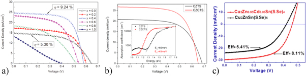
Figure 11. (a) J-V characteristics of Cu2Zn1-xCdxSnS4 thin film solar cells (x = 0–1.0). Reprinted with permission from [78]. John Wiley & Sons. (© 2015 WILEY‐VCH Verlag GmbH & Co. KGaA, Weinheim). (b) J-V curves of Cu2ZnSnS4 and champion Cu2Zn0.6Cd0.4SnS4 devices. The inset present the absorption coefficient obtained from PDS measurement. The Urbach energy (EUrbach) can be extracted from the inverse of the slop of the linear part below the band gap energy. Reprinted with permission from [79]. Copyright (2017) American Chemical Society. (c) J-V curves of Cu2ZnSn(S,Se)4 and Cu2Zn0.95Cd0.05Sn(S,Se)4 devices. Reprinted with permission from [81]. Copyright (2016) American Chemical Society.
Download figure:
Standard image High-resolution imageSimilar results were also observed by Hao et al [79], where the reported efficiency was further boosted to 11.5% by fixing the Cd substitution to 40% based on vacuum-based sputter method (figure 11(b)). Their work also showed the enlarged grain size and changed secondary phases with Cd-alloying. The band tailing problem in their work is studied by Urbach tail energy (EUrbach) model which is characterized by photothermal deflection spectroscopy (PDS). The lower EUrbach of CZCTS compared to CZTS indicates the reduced band tailing which is correlated to the decreased disorder resulting from Cu-Zn antisite defects. Additionally, the Cd alloying can also increase the minority carrier lifetime. As a result, the VOC -deficit reduced by more than 100 mV after Cd substitution [79].
It is well known that the Se-containing kesterite solar cells present less VOC deficit than that of pure sulfide [82, 83], which could possibly be attributed to the higher formation energy of Cu-Zn antisite defects in selenide kesterite [84]. In this case, the amount of Cd substitution can be controlled in a lower amount to obtain fewer antisite defects. Wu et al reported that the device performance of CZTSSe solar cell is improved from 5.41% to 8.11% by introducing only 5% Cd substitution in a solution method (figure 11(c)) [81]. The role of Cd alloying in promoting grain growth and changing charge density and depletion region width is also observed in this research. By controlling the Cd/(Cd + Zn) at 0.13, Sun et al achieved a CZTSSe solar cell with efficiency over 11% [85]. The Cd was incorporated by selenizing chemical bath deposited CdS on top of the sputtered quaternary CZTS precursors. Besides the grain size and carrier concentration change as reported previously, the trap energy level is estimated to be decreased after Cd alloying.
So far, CdS has been generally adopted as the buffer material for Cd-alloyed kesterite. For pure sulfide kesterite CZTS, ZnxCd1-xS was showed as a potential buffer option [86]. Upon heat treatment of CZTS/CdS heterojunction, ZnxCd1-xS/Cu2ZnxCd1-xSnS4 heterointerface is formed as a result of elemental inter-diffusion, where slight Cd diffuses into the CZTS surface and Zn diffuses into CdS [86]. Hao et al reported that these elemental inter-diffusion at heterojunction facilitates the formation of a more favorable band alignment of ZnxCd1-xS/Cu2ZnxCd1-xSnS4, resulting in the suppression of the heterojunction interface recombination, which promotes the efficiency of pure sulfide CZTS to over 11% [86].
4. Group III
4.1. Indium (In) and gallium (Ga)
The crystal structure of kesterites is generally derived from the wurtzite crystal structure of ZnSe in the increasing series of complexity from ZnSe–CuInSe2–Cu2ZnSnSe4 in the attempt to avoid the scarce materials In and Ga. However, the chalcopyrite ancestors of the kesterites based on Cu(In,Ga)Se2 still outperform solar cells with kesterite absorbers by far. Despite the limitation in indium abundancy it is therefore interesting to evaluate mixtures in the CuInSe2-Cu2ZnSnSe4 system and put their behavior in relation.
In recent experiments, Giraldo et al have processed CZTSe thin film absorbers by a sequential sputter and reactive annealing process [87] and studied the impact on performance of depositing small amounts of In (0–10 nm, corresponding to a maximum of up to nominal 2.6 × 10¹⁰ at cm−3) onto the metallic precursor stacks prior to selenization. The efficiency of solar cell devices was slightly decreased, mainly by a small drop in FF, suggesting that CZTSe can tolerate incorporation of small amounts of In into the crystal structure, but devices did not particularly benefit from it.
Powders along the complete compositional range from Cu2ZnSnSe4 to 2 CuInSe2 were synthesized by Schorr et al [88]. For these CuInx[Zn0.5Sn0.5]1-xSe2 materials a miscibility gap in the region 0.4 < x < 0.8 was found with a chalcopyrite crystal structure on the In-rich side of the gap and a kesterite structure on the (Zn,Sn)-rich side. Simultaneous Rietveld refinement of X-ray and neutron diffraction data revealed that mixing small amounts of Cu2ZnSnSe4 into CuInSe2 leads to a random distribution of In, Zn and Sn atoms exclusively on the 4b position of the chalcopyrite structure, while mixing small amounts of CuInSe2 into CZTSe influences all three cation sites in the kesterite structure.
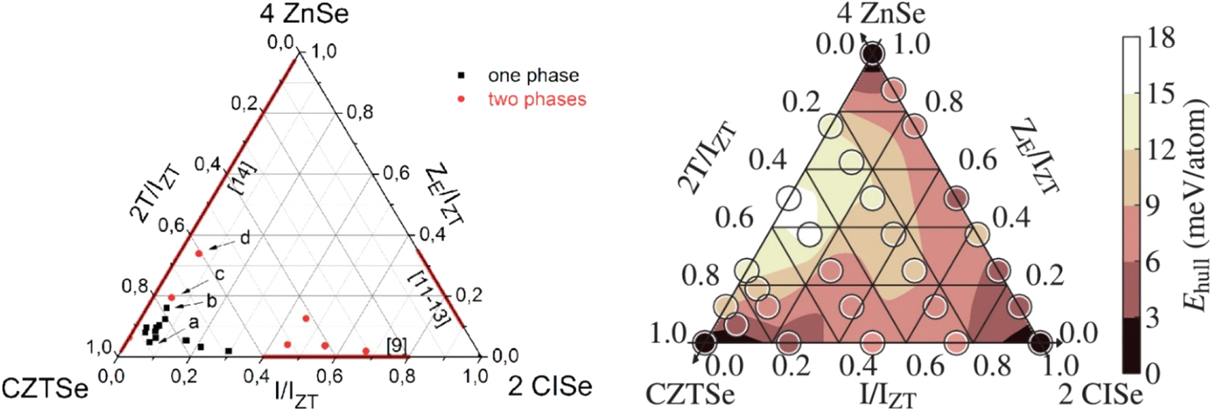
Hartnauer et al were able to reproduce the reported miscibility gap with thin films prepared by co-evaporation [90]. Here, off-stoichiometric Cu-poor Zn-rich films with typical values of [Cu]/([Zn] + [Sn]) (CZT) and [Zn]/[Sn] (ZT) ratios of 0.7–0.8 and 1.3, respectively, were used. In this work, slightly increased efficiencies due to higher short circuit current densities were found for absorbers with small amounts of In, ([In]/([In] + [Zn] + [Sn]) (IIZT) ratios of 0.07) were obtained. In pure, In-free and Zn rich co-evaporated CZTSe thin films with these ZT ratios, the presence of ZnSe secondary phases is commonly observed [90]. Interestingly, the addition of small amounts of In very effectively suppressed the segregation of this ZnSe secondary phase. In additional experiments, the absence of ZnSe segregation in the presence of moderate amounts of In was confirmed with XRD and Raman spectroscopy for absorbers with even higher ZT ratios of up to 1.83 [89]. The determined single and multi-phase regions within the 4 ZnSe- 2 CuInSe2–CZTSe phase triangle at room temperature are summarized in figure 12, where stable compositions with single phase materials are marked with a black circle and compositions showing phase separation with a red circle. On the three sides of the triangle, regions with miscibility gaps according to literature data for the three pseudo-binary compositional variations between 4ZnSe–2CuInSe2, 2CuInSe2–CZTSe and CZTSe–4ZnSe are marked by red lines. The formation energies calculated with DFT support the experimental data and predict an enhanced stability for Zn-rich kesterites if small amounts of In are mixed into the CZTSe [89]. In figure 12, the thermodynamic stability as a result of these DFT calculations is given by EHull, the distance to the convex hull of stability, in a color-coded presentation for various points of the phase triangle. The smaller the EHull (darker color), the more stable is the corresponding compound. According to these data, the introduction of small amounts of In into the CZTSe structure helps to accommodate larger amounts of Zn excess in the crystal structure and prevents the segregation of ZnSe secondary phases. Similar effects were found for the case of Ga [91].

Figure 12. (left) Experimentally determined pseudo-ternary phase diagram of the CZTSe–CISe–ZnSe system for Cu-poor and Zn-rich CZTISe alloys. IZT = [In] + ([Zn]-[Sn])/2 + 2[Sn] and ZE = ([Zn]-[Sn])/2. Red lines on the edges: miscibility gaps between the two phases at the corners as determined in the literature. Black squares: in situ XRD confirmed single phased alloys. Red circles: phase-separated alloys. (right) Calculated Ehull (circles) and their interpolation (color map). Copyright © 2016, Author(s). Reproduced by [89]. CC BY 4.0.
Download figure:
Standard image High-resolution imageIn summary, In and Ga can be incorporated into the kesterite crystal structure in moderate amounts, without harming solar cell performance. In particular, the addition of In or Ga extends the potential of the kesterite structure to accommodate Zn excess without ZnSe segregation. For higher molar ratios of e.g. [2 CuInSe2]/[CZTSe] > 0.4 , phase separation is expected [92]. On the other hand, in the extreme case of completely Sn-free Cu-In-Zn-Se samples (upper-right edge of the phase triangle in figure 12) a broad solid-solution range of compounds with stoichiometries within the Cu(In,Ga)ZnSe3-ZnSe pseudo-binary is found [93]. These alternative Sn-free, non-kesterite compounds exhibit a cubic zinc-blende structure and offer a tunable band gap from 1.1 eV (CuInZnSe3) to 2.6 eV (ZnSe), rendering them suitable for photovoltaic applications [94].
5. Group IV
5.1. Silicon (Si)
At first glance, silicon is a very interesting element for alloying with the kesterite structure. Its abundance in the earth crust is by far higher than the other kesterite elements (282 000 ppm [95] or 28%) and the oxidation state +4 is very stable. Thus, it could be incorporated at the Sn-sites of the kesterite lattice and even prevent the instability that is related to the volatility of Sn and its tendency to be reduced to the +2 oxidation state [96]. Additionally, a band gap range of up to 2.4 eV [97] should be accessible for the Cu2Zn(SixSn1-x)Se4 alloy.
However, Cu2ZnSiSe4 has the wurtzstannite structure [98, 99] and there is a considerable size mismatch between Sn and Si [97]. Although first-principles calculations predicted miscibility in a wide compositional range [97], this could not be verified experimentally. In an evaporation-based study it was found, that Si does not intermix with the kesterite lattice [100]. Only the Sn-free Cu2ZnSiSe4 could be formed, but the obtained photocurrent of complete devices was very low.
For Cu2Zn(SixSn1-x)S4 there is at least one report from Hamdi et al using a ceramic route that could form alloys up to x = 0.5 with a band gap of 1.7 eV that is ideal for an application in tandem solar cells [101]. However, no working solar cell devices have been demonstrated so far.
In addition to alloying it is worth to mention, that Si was also used in smaller quantities as a dopant for CZTSe absorbers and working solar cells were fabricated, but the efficiency was lower than for the reference and gradually decreases with the amount of Si [102].
In summary, Si can be incorporated into the kesterite lattice by substituting Sn. However, due to the high formation energy, the compounds are very challenging to synthesize. The solar cell efficiency clearly decreased with Si as a dopant and no working solar cells could be fabricated for the Cu2Zn(SixSn1-x)(SySe4-y) alloys.
5.2. Germanium (Ge)
Germanium (Ge) is probably one of the most suitable and interesting group IV elements for adding into the kesterite structure, in particular at the Sn-sites. Considering the most stable oxidation states of these two elements, +4 is more likely to occur with Ge than with Sn [103], thus avoiding presence of potentially harmful +2 oxidation states [104]. Additionally, a bandgap range from 1.0 to 2.25 eV is possible with the Cu2Zn(Sn1-xGex)(S1-y,Sey)4 alloy [97, 105–107]. Several works can be found on the Ge addition in the kesterite host, from doping levels to alloying, including partial and total substitution of Sn, and some of them are here presented.
Regarding doping strategies, Giraldo et al reported the beneficial effect of Ge as dopant in CZTSe [108], observing a large efficiency improvement for very small quantities of Ge (<0.5% relative to Sn), followed by additional studies further exploring the origin/mechanisms involved in this approach [109–112]. Firstly, a strong impact on the morphology and grain size has been observed, frequently obtaining large grains [108, 112]. This was related to the formation of Ge-Se liquid phases (at ∼380 °C) during the reactive annealing, acting as crystallization flux. Other beneficial effects of Ge have been reported, including interaction with Na with effect on the carriers concentration [111], modification of the reaction pathways minimizing Sn-Se phases formation (avoiding to a large extent the Sn loss and secondary phases formation) [112], passivation of detrimental grain boundaries related to high recombination [110], annihilation or minimization of Sn-related deep defects [113]. Through the optimization of doping strategies, by adding Ge nanolayers at the bottom and on top of metallic precursors, Ge doping has contributed to considerably reduce the VOC deficit to <0.57 V thus achieving a record efficiency of 11.8% [112].
On the other hand, alloying approaches have been also investigated recently. As in the case of doping, Ge alloying of kesterite has immediately demonstrated a great potential, with device efficiencies ranging from 6.8 to 12.3% [114–122]. Among them, it is interesting to note that the best efficiency was achieved with a relative Ge content of 39% (i.e. (Ge/(Ge + Sn) = 0.39), through the optimization of a thermal annealing containing GeSe2 [117, 119] leading to an improvement of the VOC deficit by reducing band tailing, and a reduced carrier recombination at the absorber/buffer interface and/or in the space-charge region. Collord et al studied almost the full range of possible Ge/(Ge + Sn) compositional ratios (from 0 to 90%) by preparing a continuously graded sample with combinatorial mixing of Ge and Sn containing inks [118], and achieved an 11% efficiency solar cell with an optimized 25% Ge substitution (x = 0.25) with Eg ∼ 1.2 eV), leading to a remarkable reduction of the VOC deficit. Thus, the full range of Ge substitution has been investigated to some extent, including the pure Ge compound in recent reports, demonstrating that the CZGSe exhibits also kesterite structure [123]. Among the most relevant pure Ge kesterite results, Schnabel et al reported efficiencies exceeding 5% for a sulfo-selenide CZGSSe (Eg ∼ 1.5 eV) solar cell [124], while for the selenide CZGSe (Eg ∼ 1.4 eV) compound, Sahayaraj et al published a 5.5% efficiency device with a remarkable VOC of 744 mV [125]. Intriguingly, the Ge based kesterite showed less electrical losses from band tailing/electrostatic potential fluctuations compared to Ge free devices [125, 126]. However, the main limiting factors were linked to a high series resistance, leading to imperfect current collection and a high interface recombination [127]. Trying to address these issues, a detailed optimization of the CdS chemical bath deposition has allowed achieving a record efficiency of 7.6% for a CZGSe (Eg ∼ 1.36 eV) absorber [128].
6. Group V
6.1. Antimony (Sb)
In a large study assessing over 200 solar cells, Tiwari et al concluded that Sb and Na co-doping substantially improve the efficiency of Cu2ZnSnS4 (CZTS) prepared by thermolysis of molecular precursors as exemplified in figure 13(a) [129]. The introduction of Sb as a dopant was inspired by the positive effects on grain growth previously demonstrated in CIGS [130]. In the case of CZTS, Sb was also observed to act as a recrystallization flux leading to more effective grain growth and compact films as a result of a decrease in the enthalpy of I-4 phase formation [129]. Sb doping showed an overall improvement in key CZTS device metrics such as VOC and fill factor, which comes as a result of a complex interplay of remediation of elemental disorder and improvement of band alignment. Figure 13(b) illustrates the decrease of the isotropic thermal parameter in Sn and Cu sites (as obtained by XRD structure refinement) upon Sb and Na doping, respectively, suggesting a significant decrease in disorder at these sites [129]. The effect of Sb on Sn disorder can be simply rationalized by their similar ionic radii (Sb, Z = 51 to Sn, Z = 50). Zhang et al showed by DFT SbSn exhibits smaller lattice relaxations and has lower formation energy than native CZTS defects [131]. It should be mentioned that CuSn and ZnSn antisite domain boundaries have been experimentally observed by atomic resolution transmission electron microscopy in CZTS crystallites [132]. Furthermore, DFT supercell calculations by Chen et al concluded that such antisites give rise to mid-gap traps which could be highly detrimental to device performance [6].

Figure 13. Effect of Sb and Na:Sb co-doping on CZTS bulk structure, surface electronic landscape and device performance: (a) J-V characteristics of devices under dark and standard AM1.5 G illumination (100 mW cm−2), (b) relative change in isotropic thermal parameters of the 2a (Cu & Zn) and 2b (Cu & Sn) sites in I-4 phase, and (c) distribution of local effective work-function (LEWF) over 16 μm2 with respect to effective CdS work-function. Figures (a) and (b), copyright © 2016 American Chemical Society. Reproduced from [129]. CC BY 4.0. While (c) is reprinted with permission from [133]. Copyright (2018) American Chemical Society.
Download figure:
Standard image High-resolution imageSb doping has also a strong effect on the surface electronic landscape of CZTS, as recently revealed by Tiwari et al using high-resolution energy-filtered photoelectron emission microscopy [133]. Figure 13(c) shows a substantial narrowing of the spatial distribution of effective work-function upon Sb and Na:Sb co-doping, which is another indication of a decreased elemental disorder. Sb (group V) generates donor states, which leads to a decrease of the overall work function, while Na co-doping result in a substantial work-function increase. Tiwari and co-workers also observed a grading of Sb content with a maximum concentration at the Mo/CZTS boundary of 0.069 ± 0.007 wt%, while Na co-doping led to 2.5 times lower Sb content [133]. Figure 13(c) also depicts how these trends can affect the CZTS/CdS barrier heights, which have shown a close correlation with recombination activation energies estimated by the temperature dependence of VOC in devices [133]. Interestingly, this approximation to barrier heights enable estimating CZTSSe/CdS conduction band offsets in the range of 0.3 to 0.4 eV [134], which is consistent with values proposed in the literature [135]. However, quantitative analysis of band-offsets remains a highly challenging issue in view of elemental intermixing generated in high-quality junctions as exemplified by the elegant work by Bär et al [136].
7. Group VII-B and VIII-B
7.1. Manganese (Mn)
Among transition metal candidates, Mn is one of the promising elements to replace Zn. Electron configuration in Mn is quite stable at oxidation state +2, because of the nature of half-filled 3d5-orbitals, instead of partially filled orbital in Fe, Ni or Co according to Pauli exclusion principles [137]. Furthermore, the cation radii mismatch in the 4-fold coordination between Mn2+ (0.80 Å) and Cu+ (0.74 Å) is the largest compared to Zn2+ (0.74 Å), Fe2+ (0.77 Å), Co2+ (0.72 Å), and Ni2+ (0.69 Å) [18]. Based on DFT calculations, Cu2MnSnS4 (CMTS) should be thermodynamically stable in the stannite phase with I-42m space group symmetry [12] (see figure 14). In addition, Mn also has a higher relative abundance than Zn [138].
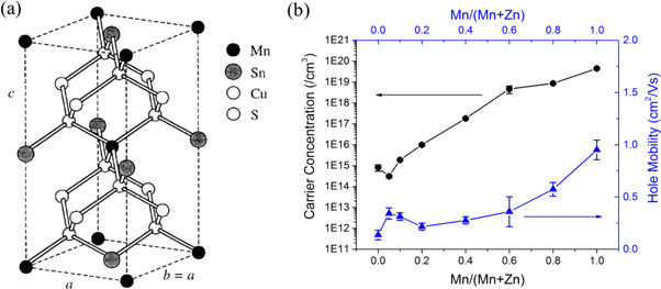
Figure 14. (a) Crystal structure of Cu2MnSnS4. Reprinted (figure) with permission from [139], copyright (1997) by the American Physical Society; (b) carrier density as a function of Mn/(Mn + Zn) in CMZTSSe. Reproduced from (2017) with permission of The Royal Society of Chemistry.
Download figure:
Standard image High-resolution imageMost of the early studies of CMTS focused on investigating its magnetic, optical and electrical properties [139, 141, 142]. In terms of solar cell application, CMTS thin film is considered as absorber layer due to its similarly high absorption coefficient (>104 cm−1) [142]. The direct band-gap of CMTS was calculated to be 1.52 eV which coincides with the measured 1.42–1.59 eV[143]. From reversible annealing treatments it was also concluded that just like CZTS disorder also occurs in CMTS.
Several studies have reported the photovoltaic performance of CMTSSe both for vacuum and non-vacuum based, even though the power conversion efficiency is generally rather poor (<1%) [144–148]. A highest conversion efficiency is 0.83% for CMTS solar cell with the ratio of Cu/(Mn + Sn) ≈0.8 and Mn/Sn ≈1.1 synthesized through two-step thermal evaporation, while the record is 0.33% for CMTSSe by sol-gel technique [149]. One possible reason for the poor performance is due to the high carrier concentration (∼1019 cm−3) [145].
In terms of partial substitution, Cu2MnxZn1-xSnS4 (CMZTS) and Cu2MnxZn1-xSn(S,Se)4 (CMZTSSe) have been fabricated by different synthesis methods and shown improvement at low Mn substitution [150–153]. The highest solar cell efficiency is achieved at 5.7% for 15% Mn in CMZTS [150], and 8.9% for 5% Mn in CMZTSSe [151]. The enhancement is attributed to the improved grain growth, better interface between absorber and buffer, and a change in majority defects from CuZn to VCu defects for CMZTSSe [150, 151]. As the amount of Mn substitution increases, the carrier concentration increased significantly (figure 14), and the radiative recombination is quenched, resulting in poor photovoltaic performance for samples with high Mn content [140].
7.2. Iron (Fe)
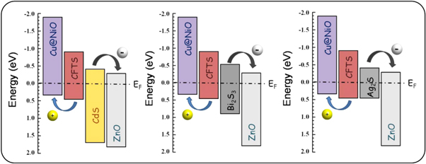
As a matter of fact, a natural mineral kesterite has formula Cu2(Zn,Fe)SnS4 [154] with an approximate content of Fe/(Fe + Zn) = 0.25. The quaternary chalcogenide Cu2FeSnS4 (CFTS) is commonly studied for its stability and the abundance and non-toxic nature of Fe. Unlike CZTS, CFTS is more stable in stannite crystal structure (ST) with an I-42m space group which shows less cationic disorder from the kesterite structure [155]. CFTS thin films have been fabricated by various methods, such as solvothermal [142], hot injection method [141], molecular method [156], spray pyrolysis [157], and mostly focused on its magnetic properties. Even though CFTS exhibit a band gap between 1–1.5 eV and high absorption coefficient (104 cm−1) in the visible spectrum range [158], there are not many reported CFTS photovoltaic devices in literature. Efficiency of 0.07% is achieved with glass/Mo/CFTS/CdS/i-ZnO/AZO by using RF magnetron sputtering to deposit the absorber [159]. A. J. Pal group managed to synthesize CFTS with SILAR method and achieved solar cell efficiency of 2.95% by replacing the CdS buffer layer with the Bi2S3 buffer [160], which exhibits a more favorable band alignment at the interface as measured by scanning tunneling spectroscopy (STS) (figure 15). As pure CFTS has a high conductivity, it is also used as counter electrode in DSSC solar cell [157, 161]. Some usage in photoelectrochemical cells (PEC) [162] and n-type absorber in hybrid organic solar cell [163] have also been reported.
Figure 15. Schematic energy level diagram of CFTS/CdS, CFTS/Bi2S3, and CFTS/Ag2S heterojunctions. The line at 0 V represents the Fermi energy after contact. Reprinted from [160]. Copyright (2017), with permission from Elsevier.
Download figure:
Standard image High-resolution image
As for the Fe alloying in CZTS, both of Fe2+ (0.66 Å) and Zn2+ (0.64 Å) have similar ionic radii, which enables a solid solubility in the Cu2ZnxFe1−xSnS4 (CZFTS) [18]. There are few studies about CZFTS thin film properties which shows transformation from kesterite to stannite and increase in band gap (ranging from 1.35 eV to 1.7 eV) as the amount of Fe increases [156, 164–166]. However, a combinatorial study using spray coating showed a strong detrimental effect on quasi-Fermi level splitting (QLFS) in Cu2ZnxFe1−xSn(S,Se)4 even at low concentrations of Fe [167]. So a possible positive role of Fe doping is doubtful as transition metals with a partially filled d-orbitals (Fe, Cr, Co) can introduce deep defect states within CZTSSe bandgap similarly to what is observed in CIGS absorbers [168, 169].
7.3. Nickel (Ni)
Another transition metal that can substitute for Zn is Ni since the ionic radius 0.69 Å for Ni2+ is close to 0.74 Å for Zn2+ [18]. Theoretical studies reported that the substitution of Ni for Zn in CZTS compound can potentially enhance electrical conductivity and reduce the optical band gap [155]. However, the defects complex in Cu2NiSnS4 (CNTS) is predicted to yield localized in-gap states based on first principles density functional theory calculations [12].
Nevertheless, CNTS has been synthesized through various synthesis method such as hot-injection, solvothermal and hydrothermal to obtain nanoparticle CNTS [142, 170–174]. CNTS has an energy band gap of 1.5 ∼ 1.6 eV similar to CZTS and a high optical absorption coefficient of ∼106 cm−1 [142, 170–174]. CNTS exhibits the zincblende crystal structure while a complementary theoretical calculation predicts the P 2c polytype as the most thermodynamically stable phase [175]. Two solar cell architectures with CNTS have been reported: a device architecture glass/Mo/CNTS/CdS/Al-ZnO/Al yielded 0.09% efficiency [175] whereas another structure utilizing ZnS coated on ZnO nanorods in the ITO/ZnO-nanorods/ZnS/CNTS/Au architecture yielded 2.71% [176]. It is not certain if the PV effect can be attributed to the CNTS absorber because comparable efficiencies were also obtained for Cu2FeSnS4 and Cu2CoSnS4 layers in the identical device structure.
8. Conclusions
8.1. What we learnt
The highest efficiency devices featuring extrinsic doping elements are summarized in tables 1 and 2, restricted to the one highest efficiency value per element (total area measurement whenever available). Without repeating dopant-specific results described in the previous sections, the following general observations can be deduced:
- 1.Several dopants have been reported to improve the performance of kesterite solar cells as compared to the nominally undoped reference devices. It is often difficult to differentiate between pure electronic effects of the dopant and other possible influences such as changes in the crystallization path leading to a different morphology, deviations in matrix composition, presence of alkali dopants coming from the substrates or atmosphere, etc.
- 2.Alkali dopants (Li, Na, K and to some extent Cs/Rb) have been proven to increase acceptor concentrations as well as to improve the morphology of the polycrystalline kesterite absorbers enabling more efficient devices. For the highest efficiency both matrix element composition and alkali dopant concentration must be carefully selected.
- 3.Alloying strategies by the isoelectronic substitution of Cu with Ag, Zn with Cd, or Sn with Ge do change the absorber bandgap as predicted within the solid solution ranges, can suppress the formation of secondary phases, and can partially reduce the disorder of the cation sub-lattice.
- 4.None of the reported doping or alloying strategies has succeeded in beating the record efficiency of the nominally 'undoped' device with 12.6% efficiency (which may contain Na-doping stemming from the glass substrate). This indicates that rather intrinsic defects are prevailing in kesterites, thus governing opto-electronic properties of the kesterite absorbers and providing an extraordinary tolerance against extrinsic doping.
Table 1. Compilation of the highest efficiency kesterite solar cells, which include extrinsic doping elements with concentration <1 mol%.
| Material | Doping element | Eg (eV) | Voc (mV) | Eff (%, total area) | References |
|---|---|---|---|---|---|
| CZTSSe | nominally undopeda | 1.13 | 513 | 12.6 | [3] |
| CZTSSe | Li | 1.04 | 449 | 11.5 | [28] |
| CZTSe | Na | 1.0 | 423 | 11.6 | [42] |
| CZTSe | K | 1.02 | 432 | 9.7 | [48] |
| CZTSSe | Rb | 0.96 | 419 | 8.8 | [28] |
| CZTSSe | Cs | 0.97 | 439 | 9.1 | [28] |
| CZTSe | In | 1.02 | 423 | 7.8 | [87] |
| CZTSe | Ge | 1.04 | 463 | 11.8b | [112] |
aUnintentional Na doping from the glass substrate cannot be excluded. bActive (illuminated area) measurement.
Table 2. Compilation of the highest efficiency kesterite solar cells which include extrinsic alloying elements with >1 mol%.
| Material | Alloying element | Eg (eV) | VOC (mV) | Eff. (%, total area) | References |
|---|---|---|---|---|---|
| ACZTSSe | Ag/(Ag + Cu) = 3% | 1.07 | 448 | 10.4 | [61] |
| CMZTSSe | Mg/(Mg + Zn) = 4% | 1.01 | 419 | 7.2 | [76] |
| CZCTS | Cd/(Cd + Zn) = 40% | 1.38 | 650 | 11.5 | [79] |
| CZTGSe | Ge/(Ge + Sn) = 22% | 1.11 | 527 | 12.3 | [119] |
| CMZTS | Mn/(Mn + Zn) = 5% | 1.055 | 418 | 8.9 | [151] |
8.2. What we need to learn
- 1.Research efforts to identify intrinsic defect(s) negatively affecting the minority carrier lifetime and diffusion length of the kesterite absorbers should be intensified. For instance, a recent theoretical study has suggested that the sulfur vacancy VS that is stabilized by the presence of Sn2+ can act as a non-radiative site [104, 177]. This should be verified experimentally, and if confirmed, efforts can be targeted to test doping/alloying strategies that compensate these defects and stabilize the normal-valence oxidation state of Sn4+.
- 2.When claiming the effectiveness of doping/alloying elements, high-efficiency reference (non-intentionally doped and/or alkali-doped) baseline samples with efficiencies > 8%–10% should preferably be used, otherwise the observed 'improvement' effect may erroneously be caused by a non-optimized baseline process.
- 3.Characterization techniques must be developed and widely used to reliably access important semiconductor absorber metrics such as the QFLS, defect concentration and their energetic position, carrier lifetime and diffusion length. This is important since common techniques such as TRPL do not yield reliable data on the minority carrier lifetime because some artefacts such as carrier trapping can affect measured PL decay times[10]. This will help to rapidly assess the optoelectronic properties of new compounds, thus assisting in search for new and effective doping/alloying strategies.
Acknowledgments
Y E R and S G H acknowledge the H2020 Programme under project STARCELL (H2020-NMBP-03-2016-720907 and SERI contract 16.0165). S G and M P acknowledge the H2020 Programme under the projects STARCELL (H2020-NMBP-03-2016-720907) and INFINITE-CELL (H2020-MSCA-RISE-2017-777968), the Spanish Ministry of Science, Innovation and Universities under the project WINCOST (ENE2016-80788-C5-1-R), and the Government of Spain for the FPI fellowship (BES-2014-068533) and the Ramon y Cajal fellowship (RYC-2017-23758). D T and D J F are indebted to the UK Engineering and Physical Sciences Research Council (EPSRC) for funding via the PVTEAM Programme (EP/L017792/1) and to the support from the Helmholtz Zentrum für Materialien und Energie Berlin, and also acknowledge the support of the colleagues and facilities acquired under various EPSRC grants including for microscopy and Brunel NanoESCA facilities at the University of Bristol (EP/K035746/1, EP/K035746/1, EP/M000605/1). X H acknowledges the Australian Research Council under project LP150100911 and ARENA (Australian Renewable Energy Agency) under project 1-USO028 and RND006. M K-K acknowledges financial support via the Estonian Ministry of Education and Research funding project IUT19-28 and the European Union Regional Development Fund, Project TK141.