
Abstract
Atomic and close-to-atomic scale manufacturing (ACSM) represents techniques for manufacturing high-end products in various fields, including future-generation computing, communication, energy, and medical devices and materials. In this paper, the theoretical boundary between ACSM and classical manufacturing is identified after a thorough discussion of quantum mechanics and their effects on manufacturing. The physical origins of atomic interactions and energy beams-matter interactions are revealed from the point view of quantum mechanics. The mechanisms that dominate several key ACSM processes are introduced, and a current numerical study on these processes is reviewed. A comparison of current ACSM processes is performed in terms of dominant interactions, representative processes, resolution and modelling methods. Future fundamental research is proposed for establishing new approaches for modelling ACSM, material selection or preparation and control of manufacturing tools and environments. This paper is by no means comprehensive but provides a starting point for further systematic investigation of ACSM fundamentals to support and accelerate its industrial scale implementation in the near future.
Export citation and abstract BibTeX RIS

Original content from this work may be used under the terms of the Creative Commons Attribution 3.0 license. Any further distribution of this work must maintain attribution to the author(s) and the title of the work, journal citation and DOI.
Abbreviations
| ACSM | atomic and close-to-atomic scale manufacturing |
| EUVL | extreme ultraviolet lithography |
| IC | integrated circuit |
| AFM | atomic force microscope |
| STM | scanning tunnelling microscope |
| DFT | density functional theory |
| SPM | scanning probe microscope |
| LJ | Lennard-Jones |
| MD | molecular dynamics |
| LDA | local density approximation |
| GGA | generalised gradient approximation |
| DFTB | density functional based tight binding |
| TD-DFT | time-dependent density functional theory |
| HDL | hydrogen depassivation lithography |
| KMC | kinetic Monte Carlo |
| ALE | atomic layer etching |
| ALD | atomic layer deposition |
| PE-ALD | plasma-enhanced atomic layer deposition |
| DNQ | diazonaphthoquinone |
| FEBE | focused electron beam etching |
| FEBD | focused electron beam deposition |
| SEM | scanning electron microscope |
| STEM | scanning transmission electron microscope |
| FIB | focused ion beam |
| NNPs | neural network potentials |
| GAP-RSS | Gaussian approximation potential-driven random structure searching |
| SNAP | spectral neighbour analysis potential |
Nomenclature

| wave function |
| n | principal quantum number |
| l | angular quantum number |
| ml | magnetic quantum number |

| spin angular momentum |
| r | position vector |
| t | time |
| i | imaginary unity |

| reduced Planck's constant |

| Hamiltonian operator |
| λ | de Broglie wavelength |
| h | Planck's constants |
| m | mass |
| v | velocity |
| U | interaction energy |

| equilibrium separation, van der Waals radius |
| r | interparticle distance |

| depth of the potential well |
| E | energy |
| V | Coulomb potential |
| p | momentum |

| scalar potential |
| A | vector potential |
| e | electron charge |
| m0 | the rest mass of the electron |
| M | mass of the atom |
| θ | scattering angle during the interaction |
| x1, x2 | positions of two electrons |
| wee , vext | soft-Coulomb potential |
| T | kinetic energy of the target atom |

| scatter angle in the centre of mass coordinate system |
1. Introduction
ACSM [1, 2] aims not only to achieve atomic-level manufacturing precision and functional feature size, but also to realise material removal, migration, or addition at the atomic or close-to-atomic scale. Therefore, ACSM opens a new era in manufacturing engineering as one of three manufacturing paradigms, namely, Manufacturing III [1]. ACSM research involves studying the fundamental mechanism, process and equipment development, and validation for cost-effective manufacturing of future-generation computing, communication, energy, and medical devices with atomic or close-to-atomic scale feature size and durable stability.
The small structures enabled by ACSM endow materials with special features resulting from quantum, electromagnetic, and thermal effects. Thus, ACSM can potentially be applied to multiple fields. First, ACSM will provide manufacturing solutions for future-generation quantum, phonics or DNA chips that cannot be offered by EUVL which is currently used for the mass production of 5 nm IC chips. This is because EUVL is soon reaching its physical limit and will not be able to handle the higher structural complexity required by future-generation chips with functional features at atomic or close-to-atomic scale. These chips are predicted to replace IC chips in the next 50 years as IC chips will experience significant difficulties in building interconnections and reducing the current leaks when they are required for further miniaturisation [3]. Second, ACSM is required for the manufacturing of single-electron transistors to realise single-electron transferability [4]. Although single-atom transistors can be fabricated in a laboratory, achieving atomic manufacturing precision and stability are still the main problems for their mass production. Two-dimensional materials such as graphene and MoS2 are excellent substrates that enable transistors to sustain stability; however, a sophisticated manufacturing method is still required to modify the strong covalent bonds and form and stabilise the expected patterns. Furthermore, new devices, such as quantum bits [5], spin-based logic devices [6], atomically binary gates [7], and single-atom memory [8], that have emerged in the past decades will also certainly boost the demand for ACSM.
Despite the practical benefits brought by ACSM, the challenges of realising ACSM are enormous, particularly when using traditional manufacturing tools. One fundamental difference from traditional manufacturing is that ACSM is governed by quantum theory, rather than classical theory. The uncertainty feature of quantum mechanics has caused two main challenges, i.e. deterministic manufacturing and product stability. First, atomic-scale resolution requires manufacturing tools to achieve effective control over atoms or atom clusters. The interactions that dominate this process are quantum mechanics. The phenomena of the interactions are uncertain in nature; as a result, ACSM can be difficult to perform and is subject to uncertainty. Second, even when atomic-scale structures are successfully fabricated, maintaining their stability is an enormous challenge. Atoms that construct atomic-scale patterns are usually accompanied by a very low atom diffusion barrier. The self-diffusion processes can easily damage structural integrity and compromise functions. In the manufacturing of single-atom transistors, atomic-scale patterns on semiconductors could decompose and migrate on the surface, like water droplets on a hot plate.
Despite these challenges, considerable efforts and investments have been devoted to atomic-scale manufacturing, and some promising progress has been made recently. Fang et al [9] reviewed experimental studies of several manufacturing methods, such as high energy beam machining, AFM nanomachining, macromolecular self-assembly, STM tip-based atom transformation, which have promising atomic and atomic-scale processing capability. Xie et al [10–12] investigated the material removal mechanism in atomic or close-to-atomic scale machining processes through molecular simulation. However, there is still no systematic analysis of the ACSM fundamentals to identify the intrinsic problems preventing its realisation; thus, this existing research gap inspired the present study.
In this paper, section 2 will introduce quantum mechanics to reveal the governing mechanics of ACSM and the difference between ACSM and traditional manufacturing. Sections 3 and 4 will classify and systematically analyse the fundamental atomic or energy beam-matter interactions that underpin ACSM. These sections will also introduce the quantum mechanical descriptions of these interactions. The manufacturing mechanisms of major ACSM processes will be revealed further in section 5 to manifest how these interatomic or energy beam-matter interactions affect manufacturing results. The relevant simulation methods applied to study the ACSM mechanism will also be reviewed to reflect state-of-the-art development. Section 6 will compare several promising ACSM processes and thoroughly discuss their features and current statuses, while the future development of ACSM will be envisaged in section 7.
2. Quantum mechanics in ACSM
This section will reveal the governing mechanics of ACSM, and it will first identify the boundary between traditional manufacturing and ACSM. Then, several quantum mechanical concepts will be briefly illustrated to qualitatively describe the atomic model, interactions, and quantum mechanical effects on ACSM.
2.1. Fundamental differences between ACSM and traditional manufacturing
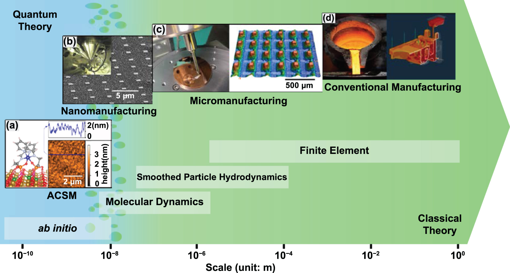
To determine the difference between ACSM and traditional manufacturing, the impact of quantum mechanical principles on the manufacturing processes must be evaluated, which includes statistical physics and quantum-based uncertainty phenomena. If the quantum effects are neglectable, the process belongs to classical manufacturing, which is governed by classical (mechanical/physical/chemical) theory. If not, it is an ACSM process, which is governed by quantum theory. However, quantum theory and classical theory are completely different in nature. The transition from one to another is neither like a boundary nor a smooth gradience [13]. Figure 1 summarises the manufacturing systems, modelling methods, and dominant theories across the length scales, and it shows that ACSM is governed by quantum theory, while micromanufacturing and conventional manufacturing are governed by classical theory. In nanomanufacturing, when the length scale is below 10 nm, quantum effects start to become more apparent [14]. When the de Broglie wavelength is larger than the system scale or inter-particle distances, quantum theory becomes dominant. Such a nanomanufacturing system is then governed by quantum theory [1].
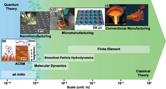
Figure 1. A length scale map of manufacturing systems, modelling methods, and dominant theories. (a) ACSM. Reproduced from [15]. CC BY 4.0. (b) Nanomanufacturing. (c) Micromanufacturing. Reproduced from [16]. CC BY 4.0. (d) Conventional manufacturing.
Download figure:
Standard image High-resolution imageClassical theory is used to describe conventional manufacturing because quantum theory normally leads to the same analytical results as classical theory, while classical theory is more intuitive and easier to understand as no quantum mechanical descriptions are involved. Dominated by classical theory, traditional manufacturing processes are often deterministic, and products are in good consistency. But in the case of ACSM, both manufactured patterns and manufacturing tools are at atomic or close-to-atomic scale, the phenomena related to quantum mechanics become apparent and are impossible to explain by classical theory unless through modification of basic quantum mechanics. Therefore, ACSM will show uncertainty features and lead to unexpected results and weak product stability, and the explanation of the phenomenon must be based on quantum mechanics.
2.2. Quantum mechanical model for atoms
Atomic modelling is the first step to discover the manufacturing mechanism taking place at atomic scale. For a single atom, the location of the electron is expressed in terms of a probability distribution. It is determined by a wave function  which describes the probability of finding an electron in an atom. The wave function is also called atomic orbitals. Depending on the type of atoms, atomic orbitals can look like a sphere, dumbbell, or clover, etc. However, each orbital has its own specialty by a unique set of quantum numbers, i.e. principal quantum number
  , angular quantum number
  , and magnetic quantum number
  . As a fermion, the electron also has a spin angular momentum of
  or
or  in a given direction, which determines two consequences under quantum mechanics. First, each orbital can only have two electrons, one has
  and the other has
  , also called Pauli repulsion. In addition, electrons will first fill orbitals with the same spin before they form pairs, named Hund's rules.
In quantum mechanics, the vector of state  is not directly related to any properties that are based on classical mechanics but is a complex function of selected state variables as coordinates and time, which can be described as
  . For instance, in solid bodies, the value
 represents the electron probability density in a certain position at a certain time. To describe the evolution of the wave function over time, the Schrödinger equation can be used and the general equation can be expressed as [17]:
where  is the imaginary unity, and
  is the reduced Planck's constant;
  is the Hamiltonian operator and represents the system's total energy, including kinetic and potential energy; it is also a Hermitian operator and its eigenvalues are real. The role of
  in equation (1) is like the force in Newton's second law because it is determined by the physical system. The precise solution of the Schrödinger equation only exists for very simple models, like a hydrogen atom. But for many other multi-electron systems, the interactions between electrons need to be added into the equation, which makes the equation impossible to solve.
2.3. Quantum mechanical effects in ACSM
The closely related wave-particle duality and uncertainty principle are two typical manifestations of quantum mechanical effects. They will compromise the accuracy of ACSM processes and leads to unexpected results. This will be explained as follows:
Firstly, quantum mechanics considered all particles as a wave, with a de Broglie wavelength of  , which can be described as:
where  is Planck's constant,
  is the mass, and
  is the velocity of the particle [18]. A simple calculation can prove that all room temperature atoms' motion can normally be described by classical physics, but electrons are often accompanied by unneglectable wavelengths because of their small mass. Therefore, the wave-particle duality plays an important role in energy beam-based ASCM processes. For example, in electron beam-based ACSM process, when an electron beam is accelerated with a voltage of 200 volts, the de Broglie wavelength of the electron is 0.87 Å. While dwelling on a graphene surface, the wavelength is more than one-third of the graphene lattice constant, which will cause more diffraction than imagining electrons as linear motion particles. To achieve ACSM, it is essential to focus the particle beam and shorten its de Broglie wavelength as much as possible, which can reduce the particle beam-matter interaction region and achieve deterministic control of an atom without disturbing other atoms around it. According to equation (2), a smaller de Broglie wavelength requires high momentum particles, i.e. particles with high accelerating voltage and large mass, which explains why particle beam-based lithographic processes prefer high acceleration voltages and large-mass particles.
Secondly, the Heisenberg uncertainty principle states that the position and the momentum of an object cannot be measured exactly, which determines the uncertainty nature of quantum mechanics. Interactions in terms of covalent bonding, Pauli exclusion and van der Waals forces, with quantum mechanics in origin will result in uncertain results in ACSM processes. The prediction of actual results under these interactions would be very difficult because these interactions are fundamentally determined by electron wave functions, which are related to the probability distribution. Here, a DFT-based first-principles method incorporating a number of approximations is commonly used to describe these interactions. Based on an initial set of trial wave functions, such calculations can use an iterative process to determine the self-consistent electron wave function that produces the system's minimum energy. Since force is a derivative of energy, this calculation also yields the force acting on each atom. In ACSM, this method is usually used to determine the lattice and electronic structures of a system with the lowest energy as well as the interaction energies and forces. For example, Sugimoto et al [19] used first-principles methods to study the mechanism for atom manipulation on semiconductors. Results demonstrated that the atomic-scale positioning of the AFM tip will modify the energy landscapes for adatom movement and the underlying mechanism is the relaxation of the tip and bond formation with the adatom [19].
3. Interatomic interactions
As reviewed in [9], ACSM techniques with true atomic patterning ability may include SPM tip-based, chemical self-limitation, light-based, and particle beam-based processes, where interatomic and energy beam-matter interactions underpin these processes. For all of these, with or without external energy sources, the interactions among atoms and between the energy beam and matters are the most important factors that affect the patterning accuracy in ACSM, particularly for the SPM tip-based atom manipulation and chemical self-limiting processes, where the interatomic interaction is the key factor that determines processing results.
Between atoms, the repulsive interaction mainly arises from Pauli repulsion; the attractive interaction can be divided into intermolecular (nonbonding) interactions (including ion-dipole and ion-induced dipole interactions, van der Waals interactions of dipole-dipole, dipole-induced dipole, and induced dipole-induced dipole), and intramolecular (bonding) interactions (including ionic, covalent and metallic bonding interactions). Their energies are shown in figure 2. In ACSM, these interactions may play important roles in generating atomic or close-to-atomic scale patterns, and their quantum mechanical effects require a proper description. Therefore, section 3 will qualitatively introduce the interactions between atoms and their descriptions in quantum mechanical terms.
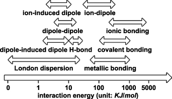
Figure 2. Comparison of the magnitude of different bonding mechanisms that bind atoms together. Data based on [20].
Download figure:
Standard image High-resolution image3.1. Pauli repulsion
It is easy to understand that there are repulsive forces between two approaching atoms. For hydrogen molecules, the Coulomb force is the main source of repulsion, but this is a special case. For other atoms, the repulsive interaction is mainly caused by Pauli repulsion, which is a quantum mechanical phenomenon with no classical analogy. To explain Pauli repulsion, imagine two helium atoms are approaching each other until their electron orbitals start to overlap. Since the  shells of two helium atoms are already occupied by two electrons, the overlapping will confuse the energy states and lead to the emergence of two electrons with the same four quantum numbers in the same orbital. This state violates the Pauli exclusion principle, so electrons will divert to higher energy states to satisfy the rules [21]. This process will cause a repulsive interaction. With the decrease of interatom distance, the repulsive 'force' ramps more quickly than the Coulomb force, which will dominate the source of repulsion in most circumstances.
3.2. Covalent bonding
Covalent bonds connect two atoms by sharing a pair or pairs of electrons. Due to the formation of a full electron shell, the energy of a shared state is lower than that of the separate atoms. Covalent bonds form in different types for different atoms, such as sigma bonds, pi bonds, polar bonds, and complex hybridisations. In diamond, sp3 hybridisation forms a very stable structure between carbon atoms with a binding energy of 7.3 eV [22]. When two atoms are identical or have similar electron affinities, the electron pair is shared equally as in the molecules of hydrogen, nitrogen, and oxygen. However, if one atom shows a higher electronegativity than the other, the electron pairs will be closer to the more electronegative one and form a polar covalent bond. The polar covalent bond will give the molecule a polarised charge distribution, making it possible to form weak bonds with other polar molecules. Examples can be seen in the water, sulphide, hydrogen chloride, etc. It is worthwhile to note that the above description only covers the general features of covalent bonds, a full explanation of covalent bonds must be based on the quantum mechanical description of electron pairs with the Schrödinger equation.
3.3. Ionic bonding
Ionic bonds form when complete electron transfer occurs between atoms, resulting in oppositely charged ions. According to the octet rule, metal atoms intend to lose their outermost electrons, while nonmetal atoms tend to accept them, both with the aim of achieving the noble gas configuration. When they meet, electrons will transfer from the metal atoms to the nonmetal ones. This results in the formation of ions, which will be bound together by electrostatic attraction. Since electrostatic attraction is isotropic, one ion can form multiple ionic bonds, which makes them very difficult to break. This explains the high hardness and melting points of ionic materials.
3.4. Metallic bonding
Metallic bonding theory argues that metals are a mixture of valence electrons, and metal cations which consist of nuclei and electrons in the inner shell. In metal, one atom can contact many other atoms and thus share the valence electrons of nearby atoms through contact. The nearby atoms will again share electrons with their nearby atoms. Thus, all valence electrons in whole metallic solid will be shared by all metal cations. Because only two electrons are allowed in an orbital, electrons will move freely among a large number of orbitals in metal. Since metallic bonds are isotropic, electron gases will attract metal cations as close as possible, leading to a close-packed crystal structure. The properties of metals, including conductivity, thermal resistance, and strength, are all related to the nature of metallic bonding interactions.
3.5. Ion-dipole and ion-induced dipole forces
In addition to van der Waals forces, ion-dipole and ion-induced dipole forces are two important intermolecular interactions. Because ions carry a stronger charge compared to dipole moments, ion-dipole and ion-induced dipole interactions can have stronger interaction energies than dipole-dipole and dipole-induced dipole interactions, as shown in figure 2.
Through electrostatic interactions, ions form non-bonding interactions with dipoles or induced dipoles. When a polar molecule is placed near an ion, their positions and orientations will be rearranged until the ion is next to the oppositely charged end of the dipole when the electrostatic attraction is at its maximum. As the dipoles are only slightly charged, the strength of the ion-dipole interactions is usually less than that of ionic bonding interactions. When an ion is placed near a non-polar molecule, the charge of the ion can temporarily induce an uneven distribution of electrons on the molecule. This temporary dipole could attract the ion and form a weak ion-induced dipole interaction.
3.6. Van der Waals forces
Van der Waals force is a distance-dependent interaction among atoms. Compared with chemical bonds in solid, van der Waals forces are weak interactions, which explains why gas hydrogen must be extremely cooled to become liquid or solid. Van der Waals forces are normally regarded as interactions that originate from the uneven or temporarily uneven distribution of electrons. Based on different types of involved particles, van der Waals forces include interactions of dipole-dipole, dipole-induced dipole, and induced dipole-induced dipole [23]. Coulomb's law can describe the first two interactions, which arise from electrostatic forces among polarised particles. Interactions between dipoles are normally weak, but when two dipoles, such as Oδ −Hδ +, Nδ −Hδ + and Fδ −Hδ +, meet, stronger interactions can be formed, which can explain the H-bonds in some materials. The induced dipole-induced dipole interactions, also called London forces, which dominate the attractions between nonpolar molecules, has a different mechanism. In fact, London forces will not exist if atoms are perfectly spherically symmetrical. However, Heisenberg uncertainty principles determine the uncertainty of electron distribution. In a short period, the charge distribution of atoms could be polar and induce the electrostatic attraction between atoms, which implies the quantum mechanical nature of London forces.
The patterning scale of ACSM indicates that van der Waals forces has considerable influence on the fabricated patterns [24, 25], particularly for 2D materials, such as graphene, MoS2, YBr3, etc, when van der Waals forces dominate the interlayer interactions. Due to the great potential of 2D materials in electronic devices, van der Waals interactions have attracted more attention in manufacturing processes.
3.7. Descriptions of interactions among atoms
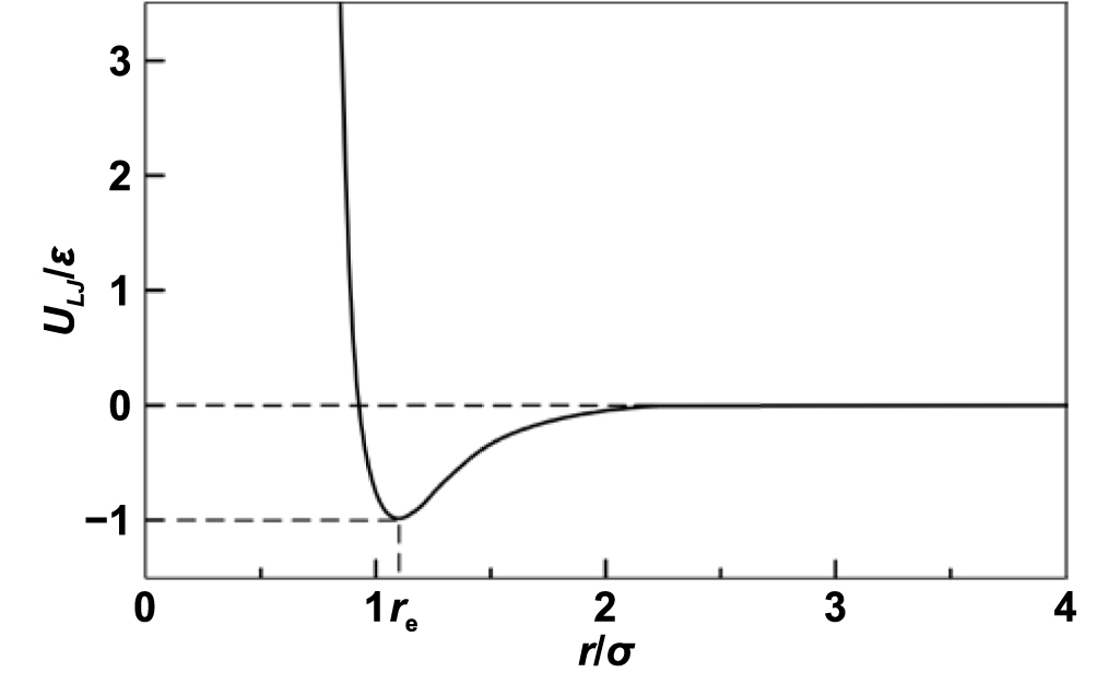
Classical physics uses Newton's second law to establish the relationship between force, position, and time. The state of a particle is governed by causality, i.e. given a certain condition, the state of a particle is predictable. The interaction between atoms can be described by potential functions, an example of LJ potential is shown in figure 3. The curve expresses the function of interaction potential to the distance of two neutral or nonpolar molecules. Considering van der Waals forces and the repulsion caused by the Pauli repulsion [26] and Coulomb force, an intermolecular pair LJ potential [27] is given as:

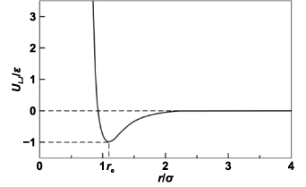
Figure 3. Interparticle interaction energy (ULJ) as a function of interparticle distance (r).
Download figure:
Standard image High-resolution imageIn the equation,  is the equilibrium separation, where
  . Here,
  is also called van der Waals radius. The minimum energy
  is at a distance of
  .
.
To describe the interactions in an atomic-scale system, various potential functions can be selected depending on the nature of atoms. The parameters in the potential functions are normally derived from quantum chemistry calculations and corrected by experiments to describe the real interactions among atoms as closely as possible. MD simulation based on these potential functions has been widely used in the theoretical manufacturing studies with scales from several nanometres to micrometres. However, this method normally fails to accurately describe the interactions in an ACSM system where the quantum mechanical effects of covalent bonding, Pauli repulsion, and electronic transfer are more pronounced. Therefore, a quantum mechanics-based method is required to describe the interactions in ACSM processes.
Quantum mechanics-based first-principles (or ab initio) methods can accurately describe the interactions for atomic-scale systems by calculating the electronic structure at every time step [28]. In principle, the basic method is to solve the Schrödinger equations for nuclei and electrons in the whole system. To describe the interactions among particles, the first-principles simulation usually applies a simpler form of the Schrödinger equation, which is the time-independent equation, the expression is given as [17]:

where E is the energy of the system. However, an intact system normally includes very complex interparticle interactions, which is impossible to solve. The calculation is usually based on a series of approximations, of which DFT is the most popular one used in computational physics, quantum chemistry, and materials science. DFT uses the functional, which is a real-valued function on functions, to determine the electronic energy and considers that the electron wave functions, which yield the lowest total energy of the system, are the correct ones [29]. The Hamiltonians in DFT contain the electrons, electron-electron interactions, electron-ion interactions, and electron exchange and correlation energies. In general, the exact functionals of electron exchange and correlation are unknown, but there are approximation methods to assist this calculation, including LDA, GGA, meta-GGA, hybrid functionals, etc. Following the approximations, the DFT method can obtain the electronic structure of an atomic-scale system that yields the lowest energy.
Between first-principles methods and classical empirical methods, there is an intermediate DFTB method, which is a semi-empirical method that is not as accurate as a first-principles method but can significantly reduce the computational cost. In the DFTB method, energy is still calculated by solving the Schrödinger equation for electrons, but the Hamiltonian matrix is not calculated by first-principles methods but parametrised by DFT calculations or experimental results. Compared with the DFT calculation, the DFTB method reduces the computational cost by orders of magnitude, while preserves the quantum mechanical nature of chemical bonding, thus allows the calculation for a relatively large system.
4. Energy beam-matter interactions
Fang et al [9] reviewed various ACSM processes, of which photon, electron and ion energy beams are popular manufacturing tools. Thus, this section examines the interactions between these energy beams and matters. Many other energy sources, such as thermal and magnetic, have potential applications in ACSM, particularly when they can be atomically applied to a system. However, to the best of the authors' knowledge, these sources are usually not taken as direct manufacturing tools but help to improve manufacturing capability. Examples can be found in thermal assisted SPM tip-based nanofabrication [30], thermal ALD [31], or magnetic field assisted machining [32].
Compared with pure mechanical tools, energy beams, such as photon, electron or ion beams, can deliver a larger density of energy to physically and/or chemically interact with material surfaces, opening the possibility for processing strong bonding materials with high efficiency. The relevant ACSM processes include photolithography, electron beam lithography, electron beam-induced modification or deposition and ion beam lithography. Due to the weak penetration and scattering features of these energy beams, the energy beam-matter interactions usually exist among a limited number of atoms or in several surface layers where atomic-scale effects become critical. Therefore, quantum mechanics plays a role in the interaction between the energy beam and substrate atoms in energy beam-based ACSM processes.
4.1. Photo-matter interactions
Photo-matter interactions can lead to observable changes in both light and matter, either matter induces changes to light, such as phonon emission, absorption, or scattering, or light induces changes to matter, such as photochemistry, thermal effect, ionisation, momentum transfer, etc. In fact, changes in both light and matter occur simultaneously which complicates the processes.
Photo-matter interaction can be divided into absorption, transmission, and reflection. For non-transparent materials, light only interacts with a few layers of atoms on the surface. The absorption in these layers, thus, dominates the photo-matter interaction.
Because of the electromagnetic feature of light, photo-matter interactions at the atomic or electronic scale are recognised as resonant interaction between oscillating electromagnetic fields and charged particles (normally electrons in atoms). To describe the time-dependent features in this process, a TD-DFT is required to provide an unbiased view of photo-matter interactions. For example, the state of an electron in a hydrogen atom can be described by the Schrödinger equation. Under the Coulomb interaction of the nucleus, the Hamiltonian is expressed as:
where  is the Coulomb potential, m and
  are the mass and momentum of the electron [33]. If the electron meets a light beam, the interaction between electron and electromagnetic field needs to be added to the Hamiltonian. The electromagnetic field can be described by scalar potential
  and vector potential
  , then the equation is shown as:
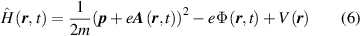
as time evolves, the wave function will change and the electron will escape from its eigenstate of the atom [33]. Under the interaction with light, if the electron is in the bound state, then the electron may just be excited and return to the eigenstate after releasing energy; if the electron is in the continuous state, then the atom is ionised. Therefore, through solving the time-dependent Schrödinger equation, the probability that an atom is excited or ionised can be calculated. However, no analytical solution exists for this equation. Even with the help of a high-performance computer, numerical solutions could be calculated but only for some simple systems.
4.2. Particle beam-matter interactions
4.2.1. Electron-matter interactions.
When an electron beam dwells on a material surface, transmitted electrons may behave differently and lead to various changes in the material. Instead of interacting with nuclei or electrons, some electrons will pass through without energy loss. These electrons are named un-scattered electrons. Scattered electrons can be categorised into two types: elastic scattering electrons and inelastic scattering electrons.
Elastic scattering electrons will interact with an atom without energy loss in total but may transfer energy and momentum to nuclei or electrons. If an electron beam impinges on an electron in an atom, the elastic scattering will create a secondary electron and ionise the atom; if on the nucleus, the momentum delivered may cause knock-on damage when electrons are accelerated by a high voltage. The energy delivered to an atom can be given as:
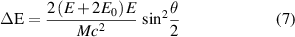
where E is the kinetic energy of the electron,  ,
,  is the rest mass of the electron, M is the mass of the atom,
  is the scattering angle during the interaction [34]. When
  is larger than the knock-on threshold, the atom will be moved out of its lattice site.
Inelastic scattering happens more often, the process can cause energy loss while passing through the substrate with the emission of x-rays, cathodoluminescence, secondary electrons, Auger electrons and visible light; at the same time the energy delivered may change the matter with the excitation (one of its electrons goes to an excited orbital) or ionisation (one of its electrons leaves the atom and becomes the secondary electron) of the atom. If the excitation or ionisation occurs on the bonding atoms, then the chemical bonds will be broken and lead to structural change.
Fundamentally, the description of inelastic scattering is rather complicated, the results depend on the energy of the incident electrons and the properties of materials. To describe the exact inelastic scattering, the time-dependent Schrödinger equation is required [35]. For a simple two-body 1D electron-hydrogen system, the expression is as follow:
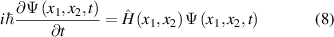
where  are the positions of two electrons [35]. The Hamiltonian of a two-electron system is expressed as:
The Coulomb interactions between electrons and between electron and hydrogen nucleus (at  ) [36] are described by soft-Coulomb interactions:
Through the numerical solution, the real inelastic scattering will be better understood and energy transfer can be calculated.
4.2.2. Ion-matter interactions.
As a beam of incident ions bombards the surface of a solid sample, complex physical phenomena occur at, above, and below the solid surface. Among these, the ion-solid scattering process is the most pronounced interaction. Fundamentally, there are two kinds of scattering processes, including the elastic scattering process where incident ions collide with atomic nuclei and transfer part of their kinetic energy to the target atoms, and the inelastic scattering process where incident ions interact with the electrons surrounding an atomic nucleus. These scattering processes have different by-products, leading to different applications.
For elastic scattering, kinetic energy and momentum are conserved during the collision process. The energy transferred from the incident ion to the target particle can be described as:
where  and
and  are the masses of the incident ion and the target particle, respectively; E and T are the kinetic energies of the incident ion and the target atom;
  is the scatter angle in the centre of mass coordinate system [37]. The relationship between the energy transfer ratio and mass ratio of the binary collision system is shown in figure 4. It indicates that the main parameters that govern the energy transfer rate from the incident ion to the target particle depend on the mass ratio of the incident ion to the target particle (
 ) and the scattering angle. For surface atoms with a T greater than the surface binding energy, they will receive enough energy from the incident ions and escape from the sample surface, resulting in a void (or a structure that accumulates a lot of voids).

Figure 4. Kinetic energy transfer rate from the incident ions to the target particles in an elastic scattering process.
Download figure:
Standard image High-resolution imageWhen an ion beam interacts with electrons in an atom, the kinetic energy could be transferred to electrons through elastic scattering or converted to other energies and absorbed by electrons or nuclei by inelastic scattering. Both processes will cause excitation and ionisation to incident and target atoms. After excitation, surface atoms can emit electrons, x-rays, and photons [38]. The inelastic process is more complicated compared with that in the electron-matter interaction because of the multiple particles and multi-step reactions involved.
5. Fundamental mechanism studies in ACSM
This section reveals the manufacturing mechanisms of major potential ACSM methods and explains how the key interatomic or energy beam matter interactions reviewed in sections 3 and 4 influence the achievement of atomic-scale precision in ACSM. The modelling methods currently used to unveil the fundamental manufacturing mechanisms will also be reviewed in this section.
5.1. SPM tip-based processes
In 1990, IBM first realised atom manipulation using a STM [39]. Since then, SPM tip-based manufacturing processes have been extensively studied. Nowadays, both STM- and AFM-based experiments have proven their atomic-scale manipulation or removal capabilities [40–43]. Their operational mechanisms will be discussed as follows.
5.1.1. STM tip-based manipulation.
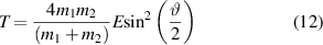
The first atomic manipulation was conducted by an STM to form the logo of 'IBM' with Xe atoms on a Ni surface [39]. After that, manipulation experiments for Ag [44], Co [45], Pt [46], CO [47], H [48], and B10H14 [49] were also accomplished in the experiment. The manipulation experiments include lateral manipulation and vertical manipulation, as shown in figures 5(a) and (b). In lateral manipulation, the adatoms can be manipulated in pulling, sliding, or pushing manners [50]. Through adjusting the tip-sample distance and tunnelling current, the lateral 'pulling' can be realised by the following procedure: (a) the conductive tip will be placed at a close distance to surfaces, so the van der Waals forces will attract the adatom to the tip; (b) when a tip is scanning the sample surface, the adatom will be pulled along the tip-scanning direction, but still bound to the surface; (c) when the adatom arrives at the desired position, the tip is retracted to a higher position and the adatom is left on the surface.
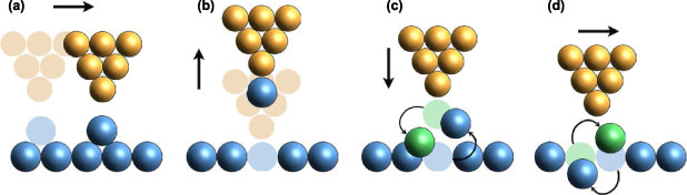
Figure 5. Schematics of SPM tip-based atom manipulation processes. (a) Vertical manipulation, (b) lateral manipulation, (c) vertical interchange, (d) lateral interchange.
Download figure:
Standard image High-resolution imageWith the help of tip-sample bias, STM can also be used in vertical atom manipulation (figure 5(b)). During the process, the adatom must overcome the energy barrier that allows the transfer from the sample surface to STM tip. As the tip gets closer to the adatom, the energy barrier will approach zero. Under the action of tunnelling current, the adatom can obtain energy from tunnelling electrons and transfer from sample surface to the tip. When the tip is lifted from the surface, the adatom will follow the tip and be pulled up. If a reverse voltage is applied, the adatom on the tip can also be transferred back to the surface when the tip-surface distance is small enough. Through this mechanism, vertical manipulation has been accomplished for Xe [51], CO [47], H [48] atoms.
In particular, the STM tip-based desorption of H-passivated Si (100)-2 × 1 [52] is also named HDL, which is one of the popular methods of atomic precision manufacturing. When the tunnelling current passes through the tip-sample gap, the Si-H covalent bonds break due to the interaction with electrons, then the hydrogen atoms escape from the surface. Through the scanning of the tip, the hydrogen atoms are thus removed from the surface site by site [53]. The position and degree of desorption can be parametrically controlled over tip scanning and tunnelling current, which opens the possibility for automation.
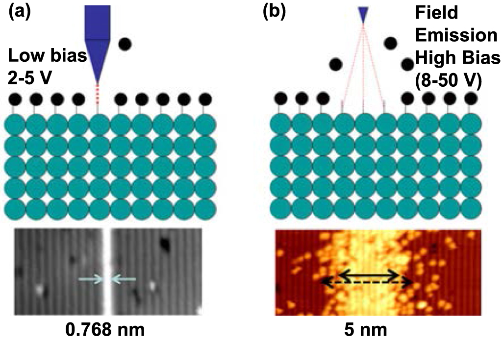
To conclude, the mechanisms of atom manipulation or removal using STM tips are as follows. For lateral manipulation, purely mechanical interactions, such as Pauli exclusion and van der Waals forces, dominate the process. For vertical manipulation, the tunnelling current provides the energy to induce manipulation. For the HDL process, the desorption of H atoms can occur in two different mechanisms under different tip-sample bias: field emission and vibrational excitation [48], corresponding to two operation modes of HDL, as shown in figure 6 [53]. One mechanism is the field emission mode under which the bias voltage normally exceeds ∼7 V. During this process, electrons will be field emitted from the tip to the sample. Because the energy of the incident electrons is higher than desorption threshold energy, the interaction will expose H atoms on the surface. In field emission mode, the tip is usually at a higher position and the exposure will occur within a large surface area, the resolution is thus limited to 5 nm [54]. Another is the atomically precise mode, which makes HDL an atomically precise manufacturing technique. It was experimentally shown that desorption occurs even when the electrons' energy is below the threshold (with a bias less than ∼5 V [53]), but the desorption rate is significantly decreased and strongly dependent on the current, which indicates multiple electrons are involved in the desorption [48]. Persson [55] has demonstrated that the atom transfer is driven by a multiple vibrational excitation mechanism with energy coming from tunnelling electrons.
Figure 6. Schematic of two modes for HDL processes. (a) atomically precise mode HDL, (b) field emission mode HDL. Reprinted with permission from [61]. Copyright (2018), American Vacuum Society.
Download figure:
Standard image High-resolution imageThe quantum mechanics-based first-principles calculation is a reliable method to describe the nuclear-nuclear, electron-electron, and electron-nuclear interactions in the atom manipulation ensemble. In previous studies, first-principles methods have been used to assist the STM tip-based manipulation with the accurate description of the relaxed atomic structures, interaction energy, the energy barriers for atom transfer, etc. These results contribute to the understanding of the process mechanisms and provide instructions on the experimental protocols. Kobayashi et al [56] studied the vertical manipulation of a single Na atom between an STM tip and a surface, the results of which indicated the tip-surface bias causes different effects on positive and negative surfaces. Quaade et al [57] studied the single-atom switch on silicon with the first-principles methods; the results showed that the electronic excitation of a localised surface resonance could explain the principal effects of controlling the switch and a higher transfer rate at a higher temperature. Nguyen et al [58] used the first-principles method to study the diffusion barrier of the Se vacancy on PdSe2, which was lower than the vacancies on MoS2 and TiO2. Xie et al [59] employed both semiempirical and first-principles simulations to study the manipulation mechanisms of a Cu adatom on a Cu (111) surface, the influence of tip height and tip structures were summarised in the results. Liu et al [60] studied the STM atom manipulation on YBr3, and the simulation determined the possibility of inserting Ti adatom into atomic pores and the energy barriers for vertical and lateral movements.
5.1.2. AFM tip-based manipulation.
Compared with STM tip-based manipulation, the AFM tip-based methods can work for more materials, including semiconductors, metals, and insulators. In 2003, Oyabu's group conducted the first atom manipulation experiment using the AFM [62] by vertically removing and depositing a Si atom on a Si (111)-(7 × 7) surface [62]. When an AFM tip indents on the sample, the interaction can remove one atom out of its equilibrium position or deposit one atom back to an existing vacancy at the surface. Later, AFM tip-based atom manipulation was also implemented in lateral directions with pulling and pushing manners [63]. Furthermore, the atom interchange mechanism was observed in the AFM tip-based manipulation experiment. The strongly bound atoms between the tip and sample may interchange both vertically [64] and laterally [65], as shown in figures 5(c) and (d). This mechanism differs from other mechanisms previously reported. Phenomenologically, atomic interchanges occur due to a reduction in diffusion barriers caused by tip-sample interactions.
Without the tunnelling current, AFM tip-based manipulation is governed by short-range interactions. Depending on the materials of tool and sample, the dominant interactions may include Pauli repulsion, ionic, covalent, and metallic bonding interactions. The quantum nature of these interactions suggests that the process needs to be described with the first-principles methods. The related simulation studies have been conducted to investigate the relaxation, interatomic interactions, energy barriers for atom transfer or interchange, minimum energy path, etc [19, 28]. Sugimoto et al [19] used the fireball code to unveil the vacancy-mediated lateral manipulation of adatoms on Si (111)-7 × 7 surface. It was found that the bonds between the adatom and the surface atoms were weakened under the tip-sample interaction. The effects reduced the barriers of atom diffusion between adjacent sites. This method was also used to explain the vertical atom interchange between the tip and Sn/Si (111)- (√3×√3) R30° surface [64], the key atomistic processes involved and the energy barriers for the manipulations were studied. Enkhtaivan et al [28] studied the tip relaxation in lateral atom manipulation. The findings indicated that the underlying physics and chemistry were the structural relaxation of the tip apex and the formation of the bonds with the diffusing adatom. Bamidele et al [66] used a combination of first-principles methods and KMC algorithm to study the dynamics and statistics for 'super'-Cu atoms on the p (2 × 1) Cu (110) :O surface. A novel mechanism that combines the atomic jump and surface diffusion was revealed.
5.2. Chemical self-limiting processes
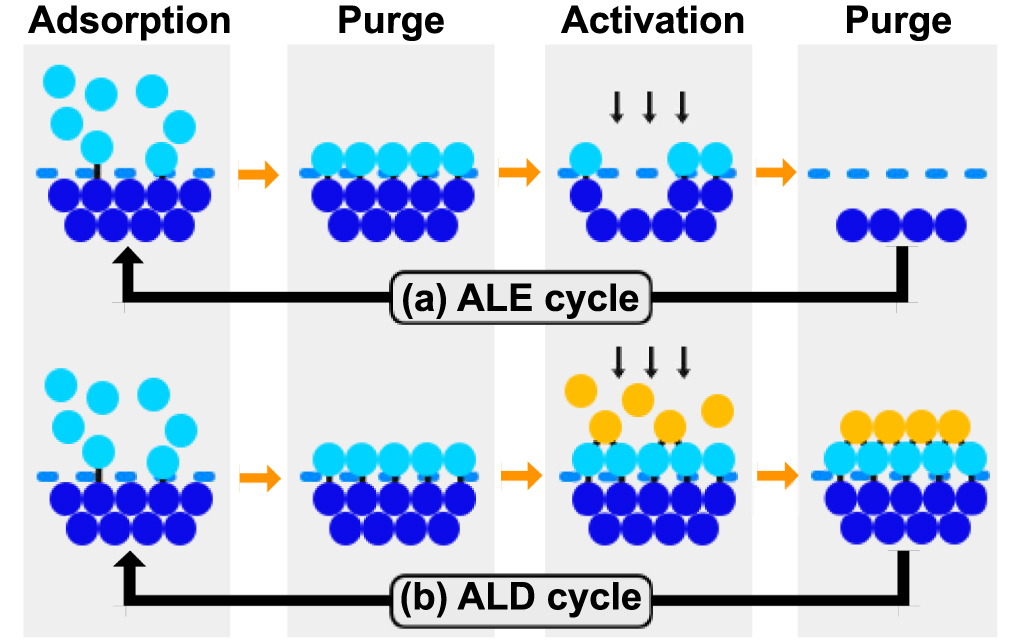
ALE and ALD are two promising techniques in the semiconductor industry, the atomic layer removal and deposition abilities are assured by materials' chemical self-limiting features.
5.2.1. ALE.
The ALE process consists of two reaction steps in each cycle, as shown in figure 7(a): the first reaction modifies the surface layer into easy-to-etch materials through the adsorption of precursors, and the second removes the reaction layer through energy species, typically a beam of low energy ions [67]. The purge processes separate these two steps to remove extra precursors and byproducts. In this process, the uppermost interlayer chemical bonds are weakened by the chemical reactions in the first process and completely broken by ionic bombardment in the second.
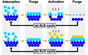
Figure 7. An illustration of self-limiting processes. (a) one cycle of an ALE process, (b) one cycle of an ALD process.
Download figure:
Standard image High-resolution imageObviously, chemical bonding plays an important role in the ALE process. To give a better understanding of the bond forming and breaking, first-principles methods have been used to evaluate the reactivity and desorption energy in ALE processes. Konh et al [68] used the DFT methods to calculate the energy required to remove Co atoms from Co (100) surfaces, the effect of surface defects on etching was also evaluated. Kim et al [69] studied the energies for Cl adsorption and Ar+-ion desorption on MoS2 to unveil the mechanism of its ALE process. Longo et al [70] studied ALE processes on an organic polymer surface using oxygen pulses. The results proved the self-limiting nature of ALE, and the fact that the formation of C–O–C bridge bonds leads to structural change.
5.2.2. ALD.
Similar to ALE, the ALD process normally involves four processes, as shown in figure 7(b). The main difference from ALE lies in the third step which introduces another type of precursor and forms a single layer of compound on the surface. As for the energy source, ALD can use thermal energy or plasma to enhance the reaction process. The PE-ALD can activate the chemical reaction even at a lower temperature with better film properties, which made PE-ALD a versatile method for nanofabrication in emerging applications [71]. In addition, the selective techniques provide a new method of ALD. Modifying the chemical properties of the surface can control the adsorption of precursors on the selected region. The selective strategies promote the formation of desired films on a surface while simultaneously avoiding deposition in adjacent regions, which is considered a 'chemical patterning' processes [72]. The selective techniques will not only eliminate the edge placement errors in semiconductor nanomanufacturing, but also bring us closer to the long-held dream of fabricating materials in a bottom-up fashion using atoms as building blocks [73–75].
The atomic-layer resolution of the ALD process relies on the chemical bonding interaction that binds the precursors and surface atoms. The chemical feature of the precursor is the key factor, the essential requirements include the volatility, reaction, self-decomposition, reactivity with substrate, dissolution, purity, etc [76]. The first-principles method has been used in previous research to study the reactivity of surface structures [77]. The purpose of the simulation mainly aims to unveil the reaction energies, atomic structures, diffusion barriers, etc [78–80]. The simulation results can contribute to the design of precursors, evaluation of reaction rates and input parameters. Furthermore, the ALD process is relative to the feature and reactor scale and normally requires multiscale modelling approaches [81]. A combined method of first-principles and Monte Carlo could address the stochastic nature, which makes it more suitable to simulate the collaborative and kinetic behaviours of the ALD process [82–84]. The results are expected to provide better control over the reactions and further optimisation of processing parameters.
5.3. Light-based processes
Photolithography is a sophisticated technique in industry and its recent advance has promoted the commercialisation of the 5 nm process. As summarised in section 4, the interaction of light and electrons in molecules is the basic mechanism of the photolithography process. Just as electrons occupy atomic orbitals in atoms, electrons in orbitals occupy molecular orbitals. When one or more photons are absorbed, an electron can transfer from one orbital to another, resulting in different outcomes depending on the atom or molecule to which the electron belongs. When an atom is excited by absorbing a photon, the electron that was activated to the high-energy orbital will normally jump back to the original orbital to sustain the ground state. However, there could be various consequences after an electron in a molecule is excited. For instance, the chemical bond will break if the electron moves from a bonding molecule orbital to an antibonding orbital. The broken bonds will leave the dangling bonds with a high chemical reactivity and induce other chemical reactions. Eventually, if the process breaks down large molecules into smaller fragments and increases their solubility, the mechanism represents positive resist lithography; if the process leads to the creation of bonds between chains and form more complex molecules, the process is called polymerising and dominates the negative resist photography.
The photochemical reaction for positive resist is illustrated in this section to describe the mechanisms of photolithography. Positive resist normally consists of three materials: a base resin, inhibitor, and volatile solvents. The inhibitor, which is a sensitive compound to light with a certain range of wavelengths, serves to impede the dissolution of resists. When exposed to light, the inhibitor will decompose due to the photochemical reaction and the process will create soluble byproducts and leave behind patterns after dissolving. For example, DNQ can absorb ultraviolet light with wavelengths from approximately 300 nm to 450 nm. The absorption bands can be assigned to n-π* (S0–S1) and π-π* (S1–S2) transitions in the DNQ molecule. The DNQ decomposes through Wolff rearrangement to form a ketene [85]. In the presence of water, the decomposition product forms an indanecarboxylic acid, which is base-soluble, as shown in figure 8. After dissolution, regions of the resist film that were unexposed to light will remain on the surface.
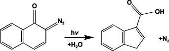
Figure 8. Photolysis of a DNQ molecule. Reprinted with permission from [85]. Copyright (1992) American Chemical Society.
Download figure:
Standard image High-resolution imageClassical photolithography is based on photochemical reactions, which has contributed to the miniaturisation of IC chips, but the theoretical limit makes it difficult to achieve atomic-scale patterns. One restriction is on the sensitivity of the photoresists. Classical photolithography normally uses resist materials that are very sensitive to laser dose, which makes the reaction region equal to or larger than the laser spot size. But a recent study [86] proposed another light-based lithographic method, where the chemical reaction is induced by the laser thermal effect, with the potential to further reduce feature size. The process utilises an inorganic resist with a higher reaction threshold for laser energy. The reaction only occurs at the centre area where the laser energy density is near the maximum, which makes the feature size equal to or much smaller than the laser spot size. Similarly, through the photothermal effect, laser beams can also be taken as an alternative to STM for H-depassivation processes [87]. An ultraviolet laser can selectively heat silicon to a temperature so depassivation can occur while maintaining a good order of atoms on the surface. Compared with SPM tip-based method, the light-based process can greatly enhance the depassivation throughput. The workflow has been experimentally demonstrated [87].
As photolithography steps into atomic or close-to-atomic scale, the atomic-scale effects of light-induced reactions become more critical. Therefore, a reliable physical and mathematical modelling method is necessary to optimise this technique. The TD-DFT has emerged in the study of the laser-induced interactions and effects, this method combines the advantages of DFT and time-dependent formalism as introduced in section 4, allowing the accurate determination of absorption spectra, photochemical reactions and excitations [88]. Waterland et al [89] calculated materials' excitation energies and transition moments in the vacuum ultraviolet. The results could assist in searching materials for photolithography at a certain wavelength range. Palma et al [90] used the TD-DFT method to explain the mechanisms of C-Br scission and C-C coupling processes in the photolithographic process of graphene nanoarchitectures. Ando [91] predicted the refractive index dispersion of fluoro-compounds using the TD-DFT methods. The results identified some materials with high refractive indices and good transparency.
5.4. Particle beam-based processes
5.4.1. Focused electron beam-based processes.
The aberration-corrected electron beam has reduced the electron beam spot to 0.1 nm3 [92], which makes the electron beam a candidate tool for ACSM processes. Like photolithography, the electron beam can also create patterns by inducing the chemical reaction on polymers. Through the interaction between electron beams and molecules, electrons in the bonds can be excited through inelastic scattering, thus breaking the bonds and changing the structure of the substrate. The electron-polymer interactions in electron beam lithography may lead to two results: the polymer chains may break down to small fragments or break off the side groups and link to other chains to form larger molecules. Normally, both reactions happen together but one of these will be the dominant process and determines the result. If irradiation causes a break in the main polymer chain so that it can be dissolved, the polymer is a positive resist. If irradiation links the chains and forms a network, making it insoluble, the polymer is a negative resist.
The inelastic scattering electron can also be applied in precursors to induce etching or deposition, a process known as FEBE or FEBD, as shown in figure 9. In these methods, precursors are introduced near the substrate and absorbed on the surface. When the compound of precursors and surface atoms is exposed to a thin electron beam, normally by SEM or STEM, the electron induced reaction will occur at the interaction region. In the FEBE process, the reaction will convert surface atoms into volatile compounds thus removing the surface atoms. In the FEBD process, the reaction will produce nonvolatile dissociation products and form the deposition. With the digital scanning of small diameter beam and proper selection of precursors and substrates, nanometre-scale structures can be created [93, 94].
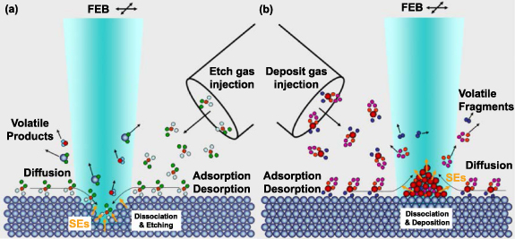
Figure 9. Schematics of (a) FEBE and (b) FEBD processes. Reprinted with permission from [95]. Copyright (2008), American Vacuum Society.
Download figure:
Standard image High-resolution imageFor 2D materials, electron beams have been used to create atomic patterns or manipulate atomic defects [96]. The mechanism is through delivering high energy to the target atom and induces the atom displacement. When the energy delivered is higher than the displacement threshold, the atom can be ejected from its lattice site and form knock-on damage. Besides, the defect atoms in 2D materials are weakly bound to substrate atoms and can be manipulated to its nearby site using a thin electron beam [97]. The underlying mechanism is that the energy delivered is higher than the atom diffusion threshold.
5.4.2. FIB-based processes.
With the development of low-temperature ion sources, current research reveals that it is able to produce ion beams with sub-nanometre spot size and a maximum current of several nanoamps [98–100]. Focused helium ion beam thus becomes a potential lithography tool for ACSM processes [101]. The helium ion source consists of a single crystal metal that is fabricated in a needle shape. The end of the needle terminates in only several atoms (up to seven atoms) [102]. Such a unique configuration enables the helium ion beam with ultra-fine spot size. In fact, the de Broglie wavelength of helium ions is smaller than electrons with the same energy (e.g. at 10 keV, the de Broglie wavelength for a helium ion and an electron is 0.1 pm and 10 pm, respectively), which indicates that helium ion beam has a higher spatial resolution than electron beam. Among all known elements, helium has the smallest atomic radius (∼1/5 of a gallium ion), which makes it easier to pass through the sample, resulting in a deeper implantation depth. The advantage is also obvious; the small atomic radius makes helium ions very difficult to be scattered near the surface, leading to a high lateral resolution, which makes it an ideal tool for imaging and nanofabrication of very thin materials (2D materials). It has been experimentally demonstrated that helium ion beam lithography can fabricate nano lines less than 10 nm width with a 20 nm pitch [103]. Due to its high spatial resolution at the surface, helium ion beams have been used in the nanofabrication of 2D materials, such as graphene [104] and MoS2 [105], etc, achieving nanometre and sub-nanometre scale structures, the mechanism is as shown in figure 10.

Figure 10. Schematic of defects created by helium ion sputtering on single-layer MoS2 on graphene/SiC. The defects include sulphur vacancies, a molybdenum vacancy, and defects in the graphene layer. Reprinted with permission from [106]. Copyright (2020) American Chemical Society.
Download figure:
Standard image High-resolution imageIn addition to subtractive manufacturing, FIB can also be used for additive manufacturing at micro- and nano-scales. FIB induced deposition, also known as ion beam assisted chemical vapour deposition, is another feature that is used extensively in FIB applications. Selected materials may be deposited onto a target surface by the introduction of appropriate gasses into the system. The deposition process was first reported by Gamo et al [107] who studied the process for the deposition of Al from Al (CH)3 and W from WF6. This technique provides the ability to deposit functional materials onto almost any solid substrate with nanometric spatial resolution. Unlike the ion sputtering process which is mainly based on elastic scattering between the ions and target atoms, the deposition process is induced by the electrons generated in inelastic scattering. These secondary electrons will break the chemical bonds of the precursor gas molecules, separated into different components: some of which remain volatile, others are deposited onto the surface. Tight beam control is critical to a successful FIB-assisted deposition since the precursor gas can easily be depleted and then cause the net deposition rate to be negative, resulting in net material removal. In order to maintain a constant positive deposition rate, the beam cannot stay at the same time point for a long time—it must move to another location and then come back to the same point to give the surrounding precursor gas enough time to replenish the depletion.
5.4.3. Simulation study.
First-principles methods have been used to simulate the particle beam-based manufacturing processes to reveal the mechanisms of particle-matter interactions. The threshold displacement energies for semiconductors were calculated in several studies [108–110], which were used to evaluate the defects generation under the interaction of particle beams [111]. The defect formations under the particle beam-matter interaction were described by either first-principles or DFTB simulation, which were used to determine the irritation and defect features of the materials [112–114]. The electronic stopping mechanisms for certain materials were investigated by a TD-DFT method, which was used to evaluate the electronic stopping power [115–117] and electronic excitations [118, 119]. Besides, the combination of TD-DFT and classical MD methods offered a simultaneous dynamic simulation of electrons and ions, which provided an unbiased insight into the interaction between particle beam and target atoms [120].
6. Discussions
6.1. Comparison
Table 1 shows the comparison of the discussed ACSM techniques above. SPM tip-based processes have a real atomic-scale patterning ability with angstrom-level control over the atomically sharp tips. The ALE and ALD methods rely on chemical, self-limiting characteristics to obtain the atomic layer resolution. The patterning resolutions for energy beam-based methods are currently around several nanometres when the energy beam-matter interaction region is well controlled; particularly, the STEM-based electron beam is a special tool that can manipulate atoms like SPM tip-based methods and realise the atom manipulation. For AFM tip-based processes, ALE and ALD, the key mechanisms that determine the atomic-scale patterning ability are the atomic interactions, such as chemical bonding, van der Waals forces, and Pauli repulsion. For the STM tip-based method, the dominant interactions also involve the interaction between the atoms and tunnelling current. The interatomic interactions still play important roles for the energy beam-based processes, but the energy beam-matter interaction would directly determine the patterning ability.
Table 1. Comparison of ACSM techniques.
| Items | Patterning scale | Dominant interactions | Modelling methods |
|---|---|---|---|
| STM tip-based methods | Atomic | Chemical bonding, van der Waals forces, Pauli repulsion, electronic excitations | DFT, DFTB |
| AFM tip-based methods | Atomic | Chemical bonding | DFT, DFTB, KMC |
| ALE, ALD | Atomic | Chemical bonding | DFT, DFTB, KMC |
| Photolithography | Nanometrics | Photochemical reaction, photothermal effect | TD-DFT |
| Particle beam-based lithography | Nanometrics (atomic for STEM based manipulation) | Excitation, ionisation, knock-on damage | DFT, TD-DFT, KMC |
As manufacturing approaches atomic and close-to-atomic scale, physical difficulties become more critical in comparison with the problems met in nanofabrication. A reliable physical and mathematical modelling method is thus in demand to address these difficulties. To reveal the underlying mechanisms of ACSM processes, we need to resort to the quantum mechanics-based first-principles method which provides a more reliable description the ACSM processes than the classical Newtonian mechanics-based methods. As reviewed in previous sections, the DFT/DFTB and TD-DFT methods are represented tools contributing to the mechanism study and process optimisation for different ACSM processes. Through descriptions of atomic structures, interaction energy, minimum energy path, and the possibility for atom transfer, the DFT/DFTB methods can reveal the underlying mechanisms of SPM tip-based processes, chemical self-limiting processes, and interatomic interactions for energy beam-based processes. The TD-DFT methods can describe the time-dependent features of light-matter and particle beam-matter interactions and provide an unbiased insight into light absorption, photochemical reactions, light excitations for light-based processes, and the electronic stopping and excitations for particle beam-based processes.
The development in the first-principles simulation has not only made significant contributions to the understanding of atomic-scale interactions in ACSM processes but also assisted in materials selection, phenomena prediction, experimental protocol, etc. However, due to the limitation of current computational apparatuses, the first-principles methods, even for DFTB, are restricted to the number of atoms and time scale that can be employed in the simulation. As a result, this limitation has hampered their applications. For the TD-DFT method, the calculation gives a comprehensive description of the electronic and optical excitations, which means it is rather time-consuming. The simulation for all of the possible excitations of the atomic transfer during an energy beam-based process is still out of reach. To conduct the simulation with larger scales in volume and time, the KMC approaches are more suitable but require a reliable parameterisation.
6.2. Discussions and future fundamental research focus for ACSM
In ACSM, determinism can be improved by increasing the patterning resolution as this enables control of a small number of atoms without disturbing other surrounding atoms. As previously mentioned, the SPM tip-based process relies on the atomic control over the sharp tip to manipulate atoms, while energy beam-based lithographic processes use thin energy beams to create close-to-atomic scale patterns by exposing resists, knocking out atoms, inducing etching or deposition. The interactions for energy beam-based methods are more complicated than using mechanical means, but in general, the purpose is to convert the spatial distribution of energy into the spatial distribution of atomic modifications in substrates, such as atomic defects, solubility change, atom deposition, etc. Energy beams and processed substrate materials can interact in different ways as mentioned above, but the attainable lateral resolution at a manufacturing zone depends on the feature size of the interaction region, where different reactions or knock-on damages may occur. Therefore, for both SPM tip-based and energy beam-based methods, minimising the interaction region is very important to enhance the resolution and determinism of ACSM processes.
When atomic or close-to-atomic scale patterns are manufactured, some measures are required to sustain their stability so that the manufactured structures will maintain their functionality. The stability of the structures could be related to the material's physical properties, the surface lattice structure, the processing history, and environmental effects. However, fundamentally, the two important determinants of stability are surface chemical reactivity and the structural properties related to lattice structure and atomic interactions. To provide long-term cyclic stability, the atomic or close-to-atomic scale structures must be specially designed or modified to consider the aforementioned factors. For example, in a study of the enhanced chemical stability of Ag overgrowth on Au nanobipyramids, Zhu et al [121] found that the existence of Au could reduce the electronic density and the chemical reactivity of nanostructures. Yu et al [122] found that the P confined in a carbon-porous structure could adapt the volume change upon sodiation/desodiation, which could be attributed to the design of stable nanoscale structures. Mowbray et al [123] proposed a substitutional doping method to stabilise TiO2 nanostructures. The increased stability was found to be attributed to the structural similarity to stable bulk rutile TiO2. Kozlovskiy et al [124] found that electronic modifications could induce defects concentration and further change the structural properties and stability.
Simulation studies have been widely conducted to reveal the mechanisms of manufacturing processes that may not be easily discovered in experiments. As previously reviewed, the first-principles and MD methods are both popularly used tools to describe the atomic-scale effects in ACSM processes. A first-principles method can provide reliable descriptions for the atomic interactions, while the accuracy is at the expense of huge computing cost, which limits the simulation system to hundreds of atoms. On the other hand, the empirical function-based MD simulation can model up to millions of atoms by supercomputers, while the high efficiency is a result of a compromise of accuracy. MD methods in particular lack the accuracy to describe the quantum mechanics-based effects. In order to solve these problems and provide an effective and reliable simulation for larger scale systems like ACSM, a number of multiscale approaches have been proposed [125–127]. Among these, the machine learning-based method has a high potential for accurately describing atomic interactions by generating machine learning-based interatomic potentials from first-principles calculations. The machine learning-based potentials, such as NNPs [128], GAP-RSS [129], and SNAP [130], can be automatically constructed by adjusting parameters to fit the reference electronic structure data as closely as possible (the procedure of GAP-RSS is shown in figure 11). Once generated, the potentials can allow an accurate simulation with low computational cost, which suggests their potential application in the simulation of ACSM processes.

Download figure:
Standard image High-resolution image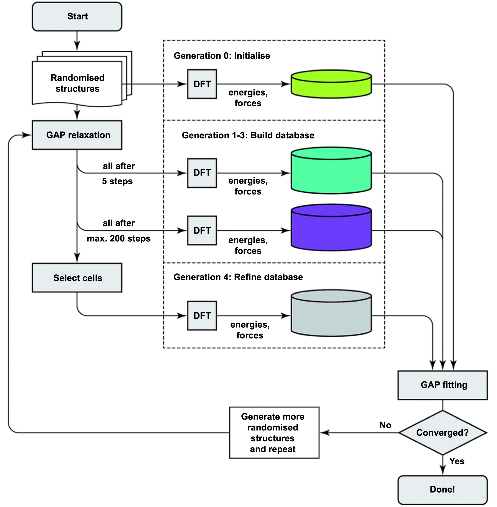
As previously reviewed, several advanced manufacturing processes have the potential to manufacture atomic-scale patterns based on different work principles for various materials, with or without external energy sources. However, ACSM is still in its infancy and enormous challenges exist in its fundamental study to achieve deterministic manufacturing and product stability. To overcome these challenges, future research should focus on the following aspects:
- A time- and cost-effective modelling approach and framework are required to support the development of ACSM. The modelling approach should be capable of providing reasonable fidelity in the simulation of ACSM process while maintaining sufficient computational efficiency. New semi-empirical potential functions or hybrid DFT-KMC modelling approach combined with artificial intelligence approach could provide such a solution.
- An effective approach is required for the selection or preparation of work materials for ACSM. Choosing or preparing suitable work materials will determine the interatomic 'force' and thus improve the probability of forming expected patterns and stabilise atomic-scale patterns. To create atomic-scale patterns, materials need to meet two conditions: (a) materials should respond to the interaction with good sensitivity because ACSM normally delivers small force or energy; (b) materials should be accompanied with relatively stable structures to maintain the atomic-scale patterns, normally with high defect diffusion barriers. Emerging artificial intelligence approaches, such as machine learning, deep learning and expert system, may provide a solution to realise effective selection and design of materials.
- The tool size or beam energy distribution directly determines the size of the interaction region. A cost-effective modelling approach to reveal the relationship between tip size or energy distribution with determinism of ASCM is necessary to control and optimise the size of the manufactured pattern and increase the probability of expected processing results. To realise practical application, research may need to focus on the development of a high-fidelity semi-empirical modelling approach to have a good level of accuracy without losing time efficiency.
- Environmental requirements for ACSM are always crucial; thus, most ACSM processes must operate under cryogenic temperatures and ultra-high vacuums to isolate external disturbances on manufacturing, measurement, and product stability. A fidelity modelling approach to reflect the influence of environment on ACSM will be helpful to overcome environmental restrictions and develop a cost-effective ACSM process that can operate under a 'normal' manufacturing environment. Further development and/or integration of current multi-physics and multi-body dynamics models will be helpful to find a potential solution to mitigate the environmental effects.
7. Concluding remarks
What distinguishes ACSM from nanomanufacturing is not only the smaller pattern with only a few atoms, but also the dominant fundamental mechanism. This paper discussed and summarised the fundamentals of ACSM processes. The atom-atom and energy beam-matter interactions were discussed in detail corresponding to the underlying quantum mechanics. The mechanisms of current available ACSM processes were summarised and the modelling techniques were reviewed to introduce the development in the simulation research. A comparison of existing ACSM processes was made in terms of dominant interactions, resolution, and modelling methods. Despite some success in experimental and theoretical research, challenges still exist in several aspects, including achieving deterministic manufacturing and product stability in ACSM. Based on the fundamental studies reviewed in this paper, future research focuses and potential solutions were proposed including the development of an effective modelling approach and framework, an intelligent material selection or preparation approach, a high-fidelity tool size and energy beam distribution control and optimisation approach and a modelling and mitigation approach for environmental effects on ACSM.
ACSM is still in its infancy. However, a new manufacturing paradigm will eventually arrive with collective effort worldwide in both fundamental and application research. It is envisaged that ACSM will significantly improve living standards due to the wide application of ACSM-enabled products, such as quantum, phonics or DNA chips, single-atom transistors, and spin-based logic devices.
Acknowledgments
The authors would like to thank EPSRC (EP/K018345/1, EP/T024844/1, EP/V055208/1), the National Natural Science Foundation of China (NSFC No. 52035009) and the Royal Society-NSFC international exchange programme (IEC\NSFC\181474) to provide financial support to this research.
Data availability statement
All data are provided in full in the reference section of this paper.