
Abstract
An investigation into the modification of low temperature deposited ZnO thin films by different annealing processes has been undertaken using laser, thermal and rapid thermal annealing of 60 nm ZnO films deposited by high-target-utilization sputtering. Single-pulse laser annealing using a KrF excimer laser (λ = 248 nm) over a range of fluences up to 318 mJ cm−2 demonstrates controlled in-depth modification of internal film microstructure and luminescence properties without the film degradation produced by high temperature thermal and RTA processes. Photoluminescence (PL) properties show that the ratio of defect related deep level emission (DLE, 450–750 nm, 2.76–1.65 eV) to excitonic near band-edge emission (NBE at 381 nm, 3.26 eV) is directly correlated to processing parameters. Thermal and rapid thermal processing results in the evolution of a strong visible orange/red DLE PL (with peaks at 590 nm, 2.10 eV and 670 nm, 1.85 eV) dominated by defects related to excess oxygen. At higher temperatures, the appearance of a green/yellow emission (530 nm, 2.34 eV) indicates a transition of the dominant radiative transfer mechanism. In contrast, laser processing removes defect related DLE and produces films with intense NBE luminescence, correlated to the observed formation of large grains (25–40 nm).
Export citation and abstract BibTeX RIS
1. Introduction
Thin films of ZnO are of interest across a range of optoelectronic and sensor device applications due to ZnO being a wide gap (>3 eV) n-type semiconductor with a high exciton binding energy [1] and a piezoelectric response [2]. Polycrystalline thin films of ZnO are deposited by a variety of physical and chemical vapour methods, with sputtering [1] being a preferred choice for low cost and scalability. However, to achieve the desired thin film properties, particularly for low temperature deposited films, it is critical to control grain microstructure, surface morphology, and internal defects [3]. Techniques that have been previously reported to improve these properties of ZnO thin films include post deposition thermal annealing [4, 5], rapid thermal annealing [6, 7], and laser annealing [8–10]. In this paper we present the results from a comparative study of the effect of all three of these annealing processes on the microstructure, crystallinity and associated intrinsic photoluminescence (PL) properties of low temperature sputter deposited ZnO thin films. The results demonstrate that pulsed laser annealing is a powerful tool for the controlled modification of low temperature deposited thin films. In particular, the work presented here explores the effect of a more comprehensive range of laser processing parameters on low temperature ZnO thin films than previously reported. The results demonstrate that five laser process regimes are achieved for different doses (by varying fluence with single pulse, or multiple pulses at various fluences) ranging from defect control to modification of grain size and texture and finally grain re-growth to produce films with intense excitonic luminescence, but with none of the material loss and additional intrinsic defect formation observed via thermal and rapid thermal annealing. The results are significant for the use of low temperature deposited ZnO thin films, for example in applications with flexible substrates, and also for work on the study of ZnO defect physics and related luminescence.
The PL emission from ZnO thin films in the UV and visible part of the spectrum are closely related to microstructure and defects [11–14]. Two significant emission peaks are typically observed: a strong, narrow UV peak (around 380 nm) due to near band-edge (NBE) excitonic emission, and a broad visible peak (in the range 450 to 750 nm) associated with deep level emissions (DLEs). In undoped ZnO films and nanostructures, the NBE emission is attributed to excitonic recombination and the DLE to a variety of intrinsic defects and defect complexes [15, 16]. Hence, the ratio of NBE to DLE peak intensities can be taken as an indication of the degree of film quality [17], since excitonic emission is highly sensitive to the presence of defects which act as non-radiative recombination centres [11, 12]. The origin of the defect related visible emission due to DLE in undoped ZnO has been attributed to various intrinsic point defects and defect complexes, but the exact origin is still a matter of some debate [18]. For the work presented here, there was no intentional extrinsic doping of the ZnO films, hence the DLE observed is attributed solely to intrinsic defects, and the strong correlation of PL with annealing treatment consequently provides a useful characterization method to investigate the effect of annealing on the defect properties.
Films deposited at low temperature were subjected to three separate annealing processes: (i) thermal anneal in air, (ii) rapid thermal anneal in nitrogen and oxygen, and (iii) laser annealing in air using single-pulse high intensity 248 nm UV KrF excimer irradiation. The results demonstrate that each of the annealing techniques has a significant effect on the polycrystalline structure, the nature and distribution of defects, and the related PL of these films; with pulsed laser annealing demonstrated as a method to control the modification of these properties to a level not previously reported in the literature.
2. Experimental
2.1. Deposition
ZnO thin films were deposited with no intentional substrate heating (max temperature attained being ∼70 °C) using a high-target-utilization sputtering (HiTUS) system (S500, Plasma Quest Ltd). HiTUS utilizes a remote, high density, plasma (1013 ions cm−3) that is generated in a side section adjacent to the deposition chamber. This side section consists of a quartz tube surrounded by a copper antennae coil. The antennae couples RF power into the argon gas at reduced pressure. Electromagnets at the exit of the side section enhance and steer the plasma onto the target. Under these conditions the argon ions have insufficient energy (between 30 and 50 eV) to sputter. The application of a sufficient negative DC bias to the target results in a high current density over the full surface area of the target. This yields high rate, uniform erosion of the target surface. HiTUS has been used to deposit low temperature metal oxides for transparent conducting electrodes [19], light emitting devices [20], surface acoustic wave devices [21] and thin film transistors [22–24].
For this work, films with thicknesses of 60 and 200 nm were deposited onto 100 mm silicon (1 0 0) substrates using a metallic zinc target (99.99% purity) in an argon/oxygen plasma at a rate of ∼50 nm min−1. Oxygen flow was set at 28, 32, 35, 38 and 41 sccm. Silicon substrates were used for this series of experiments, so that all samples could be subjected to each of the three annealing processes, including high temperature annealing. Following deposition of the films, the substrates were subsequently diced to produce samples of 1 cm × 1 cm to investigate the three annealing processes.
2.2. Post deposition annealing
Samples were either thermally annealed (TA) in a convection furnace in air, rapid thermally annealed (RTA) in a controlled environment of nitrogen or oxygen, or laser annealed (LA) in air using a pulsed excimer laser operating at 248 nm.
For thermal annealing, the samples were introduced in the furnace (Carbolite CWF1200) at the start of the ramping up period. The ramp rate was on average 25 °C min−1 and the final temperatures used were 300, 500, 600, 700, 840 and 880 °C with a dwell time of 1 h. However, ablation of the films was observed for temperatures above 700–740 °C. Hence at temperatures >700 °C, the films were put into the furnace when the process temperature was reached, and a separate series of experiments was undertaken to examine the effect of annealing dwell time on the resultant PL.
RTA experiments were carried out using an Annealsys rapid thermal processor/annealer (model AS-One). The samples were annealed in an environment of nitrogen or oxygen, bled into the anneal chamber with a flow rate of 50 sccm at atmospheric pressure. The temperature ramp rate was 20 °C s−1. Various target temperatures (600, 740, 880 and 1000 °C) and dwell times at 1000 °C (1–16 s) were used.
The LA samples were subjected to single-pulse (20 ns) laser irradiation in air using a homogenized 10 mm × 10 mm beam from a Lambda Physik LPX305i excimer laser (λ = 248 nm), at fluences in the range 135–315 mJ cm−2 (±6 mJ cm−2). A series of multiple pulse irradiations were also investigated in this fluence range.
2.3. Post anneal characterization
The films were characterized as a function of applied annealing treatment using PL, x-ray diffraction (XRD) and surface x-ray photoelectron spectroscopy (XPS). PL excitation was performed using a cw-HeCd laser (325 nm) with a circular 5 mm beamspot incident on the film surface. Typical incident beam power for the PL characterization was 9.2 mW cm−2. XRD was performed using an X-Pert Panalytical system operated in Bragg–Brentano configuration. XPS was performed using a Kratos Axis Ultra DLD with a monochromated aluminium x-ray source and delay line detection system.
3. Results and discussion
Surface XPS was used to examine the relative Zn : O ratio in the ZnO films deposited at the different oxygen flow rates. The results as shown in table 1 indicate improved stoichiometry at the higher oxygen flow rates. The extent of variation in Zn : O ratio is significant and may indicate an additional surface effect, but the overall trend is as would be expected with oxygen flow rates. Hence, films deposited at a flow rate of 38 and 41 sccm were used for the bulk of this study. These films have a typical electrical resistivity of 105–109 Ω cm.
Table 1. XPS surface characterization of Zn : O ratio for 60 nm thick films deposited with oxygen flow values shown.
| Oxygen flow rate (sccm) | 28 | 32 | 35 | 38 | 41 |
|---|---|---|---|---|---|
| Zn : O ratio | 1.36 ± 0.13 | 1.23 ± 0.04 | 1.20 ± 0.02 | 1.18 ± 0.06 | 0.94 ± 0.05 |
3.1. Thermal anneal (furnace)
Figure 1 shows the PL recorded at room temperature for samples produced from a 41 sccm wafer annealed for dwell times of up to 2 h at temperatures up to 700 °C. The PL emission is dominated by a broad defect related emission (DLE) in the visible, consistent with the orange/red emission that has been previously attributed to radiative transitions from defect sites associated with excess oxygen [25]. There is a negligible development of the UV NBE even at the higher temperatures, but the DLE increases significantly with increasing annealing temperature and dwell time. Surface XPS indicates that the film surfaces become increasingly oxygen rich with increasing annealing temperature above 700 °C, as shown for 41 sccm films in table 2. The orange/red DLE spectra was fitted with two Gaussian curves using the Peak Fit package with peaks at ∼590 and 670 nm (2.10, 1.85 eV).

Figure 1. PL of ZnO films (deposited at 41 sccm O2 flow) after thermal annealing in air at temperatures up to 700 °C. The main figure shows the effect of dwell time at 700 °C and the inset shows the effect of increasing temperature for a 1 h anneal. In all cases there is an evolution of the orange/red DLE emission.
Download figure:
Standard imageTable 2. XPS surface characterization of Zn : O ratio for 41 sccm thin films, following thermal annealing in air for 1 h at the temperatures shown. (The films annealed at 840 and 880 °C were removed from the furnace when temperature was attained, since they suffered from ablation when annealed for extended periods).
| Annealing condition | As deposit | 300 °C | 500 °C | 700 °C | 840 °C | 880 °C |
|---|---|---|---|---|---|---|
| Zn : O ratio | 0.94 ± 0.05 | 0.99 ± 0.03 | 0.99 ± 0.05 | 0.87 ± 0.16 | 0.84 ± 0.05 | 0.79 ± 0.07 |
Annealing at various dwell times was also carried out and it was found out that the PL emission did not change for periods longer than about 15 min at temperatures lower than 700 °C. At higher temperatures, however, the PL spectra changed significantly with time, with a shift in the dominant emission peak from orange to green. Since progressive loss of material is evidenced at longer anneal periods for high anneal temperatures, we also investigated the evolution of PL with time using samples from a thicker (200 nm) 41 sccm film at high temperature (840 °C). The samples were introduced in the furnace when 840 °C was reached and removed immediately after the end of each anneal period (there was a brief fluctuation of furnace temperature of ∼5 °C due to the loading process). Figure 2 shows the evolution of PL at different anneal times. The distinctive orange/red emission is developed in a very short time (30 s) and starts to decrease in intensity after 2 min. A strong green/yellow emission peaking at 530 nm (2.34 eV) develops after 7 min while after 16 min the orange/red emission is considerably reduced. The green/yellow emission reaches a maximum at 22 min after which it decreases concomitant with a visible degradation of the film. The orange/red emissions (2.10 and 1.85 eV) are usually associated with radiative transitions related to excess oxygen, primarily as interstitial (Oi) defects [26]. Hence the increase in the orange/red DLE with annealing temperature observed here could be an indication of removal of non-radiative defects through annealing, promoting the radiative transfer associated with excess oxygen defects. For the films annealed up to 700 °C, only the orange/red DLE is observed, increasing with temperature and/or dwell time. The subsequent decrease in the orange/red DLE and shift to strong green/yellow emission at the higher temperatures could indicate a change in the nature of the dominant DLE defects. It is possible that the results are indicative of a shift in dominance from Oi defects to VZn, due to the lower energy of formation of VZn defects [27]. Indeed, this transition in observed PL emission peaks at temperatures above 700 °C is consistent with a sharp deviation from surface stoichiometry as indicated by the XPS data in table 2 (however, since this occurs along with significant degradation of the film, the effect is under further investigation). Hence, there is a clear transition in the effect of annealing at temperatures above 700 °C. It is important to note that even after annealing at these high temperatures, there was negligible evidence of an NBE emission.
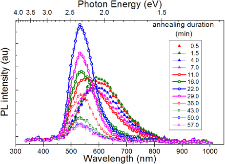
Figure 2. PL of thermal anneal in air (41 sccm sample) at 840 °C versus dwell time, showing transition from orange DLE to green as a function of dwell time. Film degradation occurs for dwell times >22 min.
Download figure:
Standard image3.2. Rapid thermal annealing
Figure 3 shows the evolution of PL at various temperatures between 600 and 1000 °C from 38 sccm samples annealed in nitrogen using RTA. As with the TA samples, there is an evolution of orange/red peak with increase in RTA temperature. With RTA, processing at the higher temperatures results in a transition of the PL to a broad visible emission encompassing both green and orange/red emissions, followed by only the green/yellow emission. RTA at temperatures higher than 800 °C also resulted in the evolution of a pronounced NBE. However, there was significant loss of material at RTA temperatures of ⩾800 °C. The magnitude of NBE observed depends on the final temperature used and the dwell period at the final temperature, but with a stronger dependence on the final temperature. Various dwell times were used at 1000 °C, with the resultant NBE increasing up to Dt = 6 s, along with a degradation of the film surface. At Dt = 16 s, the film has lost most of its material.
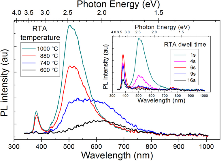
Figure 3. PL following RTA (Dt = 1 s) in nitrogen at temperatures shown (38 sccm sample), illustrating the evolution of the orange DLE peak with temperature followed by a transition to both green and orange emissions, followed by only green and NBE. The inset shows the effect of dwell time on the NBE at 1000 °C.
Download figure:
Standard imageAt 600 °C the orange/red DLE can be deconvoluted using two Gaussian peaks at about 590 nm (2.1 eV) and 670 nm (1.85 eV) respectively, similar to the results from the thermal annealing experiments. However, at temperatures ⩾740 °C a third component with a (green) peak at 505 nm (2.5 eV) is necessary to be added, which is absent in the thermally processed samples and which becomes stronger at higher RTA temperatures. Any further increase in temperature, up to 1000 °C and Dt = 1 s, results in an increase of the broad green/yellow peak and increasing loss of material (again, similar to the effects produced at thermal annealing temperatures >700 °C).
Samples from the same wafer were annealed using similar process sequences in oxygen. For the films annealed in oxygen, only the orange/red peak is evident, as shown in figure 4, which would be consistent with the emission being attributed to defects related to excess oxygen. Hence, the evolution of the green/yellow peak for RTA in nitrogen is likely to be a result of the change in the Zn : O ratio of the films and the balance of resultant intrinsic defects.

Figure 4. PL following RTA (Dt = 1 s) of 38 sccm film in oxygen, showing the dominance of the orange DLE peak even at the higher temperatures.
Download figure:
Standard imageTo investigate this further, the effect of film stoichiometry was examined. Figure 5 shows the PL from samples grown at 41, 35 and 28 sccm of oxygen that were annealed at 880 °C and Dt = 1 s in either nitrogen or oxygen. It is evident that the green/yellow DLE is present for all three samples when processed in nitrogen, but not when processed in oxygen. The intensity of all of the DLE emissions shows a strong dependency on the stoichiometry of the as-deposited sample—with consistently lower intensities for the samples that were deposited at the lower oxygen flow rates.

Figure 5. PL following RTA at 880 °C, Dt = 1 s in oxygen and nitrogen environments, comparing the stoichiometric 41 sccm samples with the non-stoichiometric samples that had been deposited at lower O2 flow rates.
Download figure:
Standard imageA green DLE has previously been attributed to both oxygen vacancies and zinc vacancies. For the results shown here, the lower sccm samples (i.e. with higher Zn : O ratio as per table 1) produce lower intensity DLE peaks in the resultant PL. This would be consistent with a reduced density of Oi defects at lower annealing temperatures, and potentially a lower concentration of VZn defects at the higher annealing temperatures, due to the higher relative concentration of Zn. Annealing in oxygen increases oxygen adsorption which in turn could be incorporated in the ZnO matrix as oxygen interstitials and antisites (with concomitant decrease of oxygen vacancies). The resultant PL indicates activation of these defects when processed in oxygen rich conditions, in a manner similar to that observed for TA films in air. It is known that in polycrystalline ZnO films oxygen adsorption can occur along the grain boundaries with an increase in the grain boundary defect concentration [28]. Hence the lack of NBE exhibited here for films annealed in oxygen is consistent with the effect that would be produced by an increased number of defects acting as non-radiative recombination centres.
3.3. Laser processing
The PL spectra of the as-deposited and LA 60 nm thick 41 sccm ZnO samples are shown in figure 6, for single-pulse processing. Two significant emission peaks are observed: a strong, narrow UV (381 nm) NBE peak and a broad orange/red DLE (440–800 nm). The observed nature of both emission peaks is highly dependent upon laser fluence applied, and five 'process regimes' are apparent for the single-pulse irradiation investigated, as shown in figure 7: (1) as-deposited material shows little emission from either peak; (2) for low fluences (up to 220 mJ cm−2) there is an increase in the intensity of the DLE peak with no significant NBE peak observed; (3) between 220 and 244 mJ cm−2 the DLE peak decreases until it becomes insignificant, while, simultaneously, the NBE peak starts to emerge significantly at 244 mJ cm−2; (4) the NBE peak continues to increase in intensity as the fluence is increased through a 'high' window up to 295 mJ cm−2; (5) finally, at 'very high' fluence of 315 mJ cm−2, there is a dramatic decrease in the NBE, which is associated with material loss. (Note, the small peak at 762 nm in figure 6 is a harmonic artefact of the measurement due to the strong NBE peak at 381 nm).

Figure 6. PL from 41 sccm samples following single-pulse laser annealing at the fluences indicated; the results at low and medium fluences show the development of an orange DLE peak, then reduction of the DLE and evolution of a strong NBE, peak at higher fluences.
Download figure:
Standard image
Figure 7. Normalized peak PL intensity as a function of LA fluence following single-pulse irradiation of 41 sccm samples, showing the five process regimes achievable by selecting fluence.
Download figure:
Standard imageFor the results presented here, the negligible detection of NBE and DLE luminescence in the as-deposited and the low fluence samples is postulated to be due to the dominance of non-radiative recombinations, which are expected to occur mostly in the vicinity of grain boundaries [29]. With increasing laser fluence (process regime 2), the crystallinity of the ZnO film improves, which would lead to a reduction in the density of non-radiative defects, and consequently the DLE becomes detectible, similar to as observed for thermal and RTA processing. At low and medium fluences (up to 256 mJ cm−2) these point defects and defect complexes are reduced, with no DLE observed in samples exposed to fluences higher than 256 mJ cm−2. Interestingly, there is no evidence of the separate green/yellow peak that was observed for the thermal and RTA samples at higher process temperatures. The effect of laser processing (at the higher fluences) is consistent with a reduction of intrinsic defects, which is in contrast to both thermal and RTA processing where generation of new defects is detected in the latter cases.
The effect of single-pulse laser processing as a function of as-deposited film stoichiometry is shown in figure 8, with clear evidence that the intensity of DLE is related to initial oxygen concentration, which is similar to observations for the samples processed by RTA. Figure 9, however, shows no DLE for the laser processed 28 sccm (Zn-rich) sample, but a clear evolution of NBE. This is further indication that the laser processing reduces the effect of non-radiative defects to allow radiative transfers from the excess oxygen defects (for films deposited at O2 > 28 sccm).
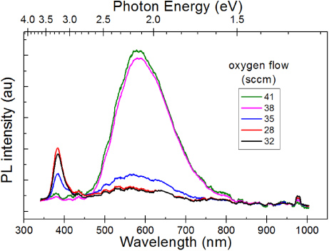
Figure 8. DLE PL of 41, 38, 35, 32 and 28 sccm LA films processed at 235 mJcm−2, showing variation in orange DLE consistent with excess oxygen concentration variation by growth condition.
Download figure:
Standard image
Figure 9. PL from a 28 sccm sample following single-pulse LA at fluences shown. No orange DLE is evident, consistent with lack of excess oxygen related defects.
Download figure:
Standard imageThe evolution of PL was also investigated by using multiple pulses at various laser fluences. At low fluences (<170 mJ cm−2) no PL peak was observed even after 100 pulses. At medium fluences (<260 mJ cm−2) an increase of NBE was observed to an optimum number of pulses related to fluence level used. Hence, laser irradiation is shown to lead to a reduction of defects as a function of total delivered dose, with the rate of defect reduction determined by the fluence used. An example set of results for multiple pulses at 235 mJ cm−2 is shown in figure 10.

Figure 10. PL from 41 sccm samples following multiple pulse LA at medium fluence, 235 mJ cm−2.
Download figure:
Standard image3.4. Structural results
The XRD patterns of selected films are shown in figures 11, 12 and 13 for the three annealing methods used. In all cases, the results indicate c-axis orientation, as indicated by the (0 0 2) peak, with changes in peak intensity and diffraction angles as a function of annealing, indicating changes in crystal structure and resultant film stress. All the films investigated are polycrystalline in nature, with annealing resulting in an increase in (0 0 2) peak height and a shift in 2θ, indicative of a transition from compressive to tensile stress. For example, for the TA samples, figure 11 shows the XRD peak intensity increasing with annealing temperature (up to 840 °C) with concomitant modification of stress from compressive (for the as-deposited film) to increasingly tensile. At the higher temperature of 880 °C, the induced stress increases further, but grain growth does not increase. A similar transition of stress from compressive to tensile followed by increasing grain size (as indicated by the reduced FWHM) is also evidenced for the RTA samples as is shown in figure 12.

Figure 11. XRD patterns from a TA 41 sccm film, showing the effect of annealing at increasing temperatures.
Download figure:
Standard image
Figure 12. XRD patterns from a 38 sccm film following RTA in nitrogen at the temperatures and dwell times indicated.
Download figure:
Standard image
Figure 13. XRD patterns from 41 sccm sample following single-pulse LA at fluences indicated. Inset shows detail of (0 0 2) peak as a function of LA fluence.
Download figure:
Standard imageFor the laser processed films, figure 13 shows that as fluence increases there is minimal grain growth and the films relax to neutral stress with the out of plane lattice constant, c close to the indexed value (2θ = 34.422°, c = 5.207 Å) at around 220 mJ cm−2. There is then a continuous increase of (0 0 2) peak intensity as fluence increases to 270 mJ cm−2 with a change to tensile stress. Between 209 and 220 mJ cm−2 a lateral spread of the (0 0 2) XRD peak and shift towards higher 2θ values indicates the existence of mixed crystallite growth through the film depth. For the films studied, the corresponding lattice constants, as determined by the (0 0 2) peak position, range from c = 5.234 Å to c = 5.158 Å as the internal stress changes from compressive to tensile.
Further confirmation of substantial grain re-growth and improvement of crystallinity with concomitant reduction in defects by laser processing is evidenced from cross-sectional TEM studies. Examples of dark field images for laser processed (single-pulse) samples are shown in figure 14. The as-deposited film, figure 14(a), is polycrystalline with a columnar grain structure, a mid-height grain width variation between 10 and 15 nm, and a high in-grain defect density. In figure 14(b) the low and medium fluences are seen to produce a more disrupted grain morphology with grains of various sizes and forms. The mid-height grain diameter variation is between 10 and 40 nm and the defect content remains reasonably high. Figure 14(c) illustrates the effect that occurs at the high fluences. The resultant coarse grain morphology is characterized by uniform columnar grains with widths between 15 and 25 nm, very thin grain boundaries, and a low defect content. In terms of the effect at the surface, XPS measurements show a Zn : O ratio of 0.9 ± 0.05 across the unprocessed substrates which remains unchanged after laser processing, hence indicative of the dominance of a bulk effect.
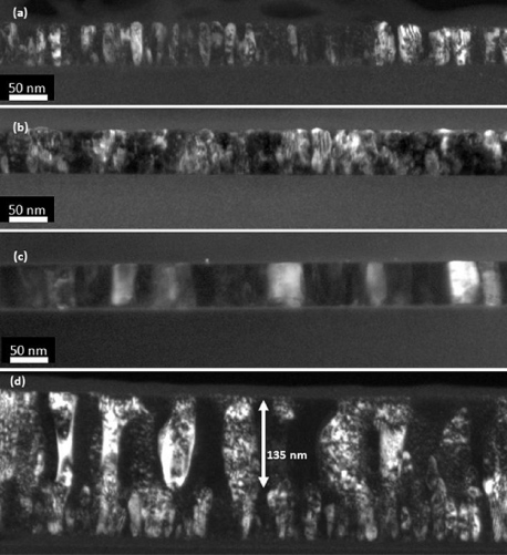
Figure 14. Cross-sectional TEMs of 60 nm thick 41 sccm sample following single-pulse LA; (a) as-deposited, (b) medium fluence, (c) high fluence. (d) shows the effect of high fluence on a 200 nm thick film, with localization of the modification effects to the upper 135 nm.
Download figure:
Standard imageFor the 60 nm thick films, the photonically induced changes in microstructure are uniform through the film thickness. However, for the 200 nm film, which is thicker than the absorption depth of the 248 nm irradiation, there is a clearly defined transition region at 135 nm from the surface below which no significant grain growth has occurred, figure 14(d). This highly localized in-depth modification is an important demonstration of the control possible when using laser irradiation, with the benefit of isolating the processed region from the substrate (or any sensitive underlying interfaces or devices).
4. Summary
In summary, an investigation of the modification of low temperature deposited ZnO thin films by the application of three different annealing processes has been undertaken. The use of thermal processing and rapid thermal processing results in the evolution of a strong visible orange/red PL emission (DLE) that is dominated by defects related to excess oxygen. This is corroborated by the enhancement of the DLE for samples processed in oxygen. At higher temperatures, the appearance of a green/yellow emission indicates a transition of the dominant radiative transfer mechanism from that due to excess oxygen defects for both TA and RTA. However, with the RTA process, higher temperature annealing produces a component of the green/yellow emission at 505 nm, which is not observed in the thermal process. In terms of the nature of the defects related to these green emissions, evidence from the effects produced by annealing samples with different starting stoichiometries points towards the formation of VZn at the higher RTA temperatures, since the samples deposited at lower oxygen flow rates (higher Zn : O ratio), exhibit the weakest DLE. Hence, this is potentially indicative of the dominance of the VZn defect over VO, which would be consistent with the lower formation energy of the zinc vacancy defects. The evolution of a significant NBE following RTA at high temperatures could be attributed to the reduction of defects at grain boundaries, but this occurs along with the transition from orange/red DLE to green/yellow DLE. Furthermore, for both thermal and RTA processing, higher temperatures result in significant film degradation and loss.
The results from the laser processing are more encouraging in terms of demonstrating a technique for controlled in-depth modification of internal film microstructure, defect density, luminescence properties, surface morphology and internal strain/film stress, without the film degradation produced by thermal and RTA processing. The effect of laser dose (by varying fluence with single pulse, or multiple pulses at various fluences) is to modify the internal properties of the film within a clear set of controlled process regimes (as shown in figure 7 for single-pulse irradiation). The resultant DLE/NBE emissions are directly correlated to processing parameters, and there is evidence of in-depth localization of the effect, consistent with the optical absorption properties of the films. This demonstrates a powerful method to investigate the defect physics versus electro-optical properties of this important material, and more significantly, a method that could be applied to films deposited at low temperatures onto thermally sensitive substrates.
Acknowledgments
The authors acknowledge the support provided by the Centre for Advanced Photonics and Electronics (CAPE) through the HiMo Project and the EPSRC through Grants EP/E023614/1 and TS/G001960/1. TEM measurements were performed by Dr Simon Newcomb (Glebe Scientific Ltd). XPS were performed by E Smith at the University of Nottingham via EPSRC grant EP/F019750/1, and we would like to thank David Taylor and Jasbinder Chohan at the University of Nottingham for RTA processing.