
Abstract
Fully transparent indium–tin-oxide/high-k-rare-earth-oxide Eu2O3/F-doped SnO2 devices that show stable bipolar resistance switching have been successfully fabricated. In addition to the transmittance of above 86% for visible light, high resistance ratio, good data retention and initial forming-free resistance switching behaviour were obtained in the transparent memory. The results of high-resolution spectroscopy and x-ray photoelectron spectroscopy analyses combining with the temperature dependence of resistance suggest that metallic Eu filaments are formed in the low-resistance state. Mechanism analysis indicates that the coexistence of oxygen vacancies and metallic Eu in the Eu2O3 films plays an important role in the forming-free resistive switching performance. The switching mechanism was attributed to formation/oxidation of filamentary and oxygen ion migration.
Export citation and abstract BibTeX RIS
1. Introduction
Potential technological advances from visible transparent circuits have aroused extensive interest and motivated various studies [1, 2]. Progress has been made by using wide-bandgap semiconductors or nanowires to construct transparent transistors [3, 4]. For the realization of a fully integrated transparent circuit, high transparency is also desirable in one of the other circuitry elements: the memory unit. Recently, resistance random access memory (RRAM) based on reversible resistive switching (RS) behaviour has attracted considerable interest for the next-generation nonvolatile memory devices [5, 6]. Many candidate materials have been reported for RRAM devices including binary transition-metal oxides (TMOs) [7, 8] and perovskite-type oxides [9, 10]. In the TMO-based RRAM devices, a so-called 'electroforming' process under a high voltage is generally needed for the fresh devices to achieve reversible RS [11]. The electroforming of RRAM is an electroreduction and drift process triggered by an electric field and enhanced by electrical heating [12]. However, this process requires a higher bias and may cause unstable resistance states, which makes RS characteristics very difficult to modulate. Up to now, the underlying mechanism of the forming-free RS behaviour and its relationship to the microstructure of RS materials are not very clear yet. Further investigation on this aspect is still required.
After the demonstration of resistance switching in structure of IrOx/high-kx/W by Prakash et al, improved memory performance using different high-k oxide such as AlOx, GdOx, HfOx and TaOx in IrOx/high-kx/W structures has been reported [13]. Eu2O3 is a well-known rare-earth (RE) metal oxide, having high resistivity, high dielectric constant, large bandgap (4.4 eV) [14], and is widely studied as a promising high-gate dielectric material for future CMOS technology. Up to now, the application of Eu2O3 in fully transparent RRAM has not been addressed in detail.
In this paper, a fully transparent sandwich structure device, indium-doped tin oxide (ITO)/Eu2O3/fluorine-doped tin oxide (FTO), has been deposited by the pulse laser deposition (PLD) technique. In addition, the conduction behaviours of both the low-resistance state (LRS) and high-resistance state (HRS) in the ITO/Eu2O3/FTO structures, together with the underlying mechanism of the forming-free phenomenon, are discussed.
2. Experimental
Eu2O3 thin films of 200 nm thick were deposited on FTO substrates at 300 °C by PLD. The base pressure of the chamber was pumped below 2 × 10⁻⁴ Pa by a molecular pump. During depositing, a KrF excimer laser (λ = 248 nm) with an energy density of 1.2 J cm−2 and a repetition rate of 2 Hz was employed. Subsequently, the wafer was annealed in air for 400 s at 650 °C by rapid thermal annealing. In order to measure the electrical properties of the Eu2O3 films, ITO top electrodes of 200 µm in diameter were deposited at 300 °C by PLD with a metal shadow mask.
The optical transmittance of the sample was measured on a Carry-5000 spectrophotometer in the wavelength range from 200 to 800 nm. X-ray photoelectron spectroscopy (XPS) was employed to determine the chemical bonding state of Eu2O3 thin films. Selected-area electron diffraction (SAED) analysis in transmission electron microscope (TEM) was characterized by high-resolution TEM (FEI, TECNAI G2 F20). The current–voltage characteristics of the ITO/Eu2O3/FTO structure were also measured by Keithley 2400 source meter unit.
3. Results and discussion
To quantitatively evaluate the transparency, the optical transmittance of the TRRAM device was investigated and is indicated in the inset of figure 1(a). The average transmittance of the TRRAM device (eliminating the substrate's contribution) is about 87% in the visible region (400–800 nm in wavelength), indicating an excellent transparency of the RRAM device.

Figure 1. (a) Typical I–V characteristics of ITO/Eu2O3/FTO memory device in semilogarithmic scale. The inset presents the transmittance of ITO/Eu2O3/FTO TRRAM device. (b) The 1st, 50th, 100th, 150th, 200th, 250th and 300th I–V curves of the device are extracted during the total 300 dc sweep cycles.
Download figure:
Standard image High-resolution imageTypical I–V characteristics performed with a 0.3 V s−1 scanning rate are shown in figure 1(a), where the arrows indicate the operations of the RS cycle. The curves exhibit nonlinear and asymmetry characteristic, indicating the device has a bipolar resistance switching behaviour. It was noted that the forming process for activating the RS typically observed in metal oxides based RRAM was not observed in our transparent RRAM. When the positive voltages applied on the ITO electrode exceeds a certain value (∼+5.7 V), the device switches from HRS to LRS. This process is called a SET process. The RESET process of the device can be achieved by sweeping the voltage to a certain negative voltage (∼−7.2 V). Our Eu2O3 films show somewhat higher switching voltages and current than those of TMOs. Kim et al considered that these differences in switching voltage may result from the larger size of the Eu2+ or the Eu3+ ion in the lattice or from the different electronic properties of f electrons and d electrons. [15] Moreover, Sebastian et al reported that the threshold switching voltage increases almost linearly with increasing sample thickness [16]. The thickness of Eu2O3 thin films (∼200 nm) was larger than those of TMOs [7–10]. Therefore, the high switching voltages and current in Eu2O3 films might be related to the properties of Eu ion and the thickness of Eu2O3 films. Further investigations are necessary.
To reveal a degree of I–V characteristic variations during the repeated cycles, 300 consecutive measurements were performed and shown in figure 1(b). The memory cell shows little degradation after 300 cycles, ensuring that the switching between HRS and LRS is highly repeatable and reliable.
In order to understand conduction mechanism of the RS device, the I–V curve is redrawn in a log–log scale. As shown in figures 2(a) and (b), the LRS both in SET and RESET operations show a typical Ohmic current. However, it seems that an entirely different current mechanism is dominated in the HRS. In figure 2(a), first a I ∝ V then a I ∝ V2.73 relationship in the SET operation could be attributed to trap-controlled space-charge-limited conduction (SCLC) [17]. In the RESET operation, the I–V was fitted to Ohmic conduction with a slope of approximately 1 in the low-voltage region (figure 2(b)), and the linear relation was consistent with the Schottky emission model in the high-voltage region (figure 2(c)) [13].

Figure 2. The I–V curves of the ITO/Eu2O3/FTO memory cell plotted in double logarithmic scale of (a) the SET operation and (b) the RESET operation. (c) HRS for the RESET operation at high-voltage regions was consistent with Schottky behaviour.
Download figure:
Standard image High-resolution imageThe dependence of the resistance on the temperature is an effective way to reveal the transport properties and conduction mechanism [18], thus, we test the resistance characteristics of the ITO/Eu2O3/FTO device under various ambient temperatures. Intentionally, before the measurement of resistance the device assembled circuit was driven by a continuous sweeping voltage to first switch on and then terminate at the switching off state. Measuring with 100 mV, the R–Time curves of the LRS from room temperature to 180 °C were obtained and are shown in figure 3(a). The value of the resistance increases gradually as the temperature increases, indicating a typical characteristic of the electronic transport in metals. Figure 3(b) shows the temperature dependence of the LRS resistance, which can be linear-fitted with a positive slope. The temperature dependence of the metallic resistance can be expressed as R(T) = Ro[1 + a(T − To)], where Ro is the resistance at the reference temperature To, and a is the temperature coefficient of resistance. By choosing To as 300 K, a of the Eu2O3 memory device in the LRS can be calculated as 7.44 × 10⁻³ K−1. Figure 3(c) shows the dependence of resistance on measurement time of the HRS at different temperature. The value of the resistance decreases gradually as the temperature increases, which could be ascribed to a typical semiconducting behaviour. Moreover, the RS behaviour of the ITO/Eu2O3/FTO device is still dynamic at 180 °C, demonstrating good memory reliability at elevated temperatures. Furthermore, by employing an Arrhenius plot, the thermal activation energy, Φt, of the ITO/Eu2O3/FTO device in the HRS are calculated. As shown in figure 3(d), the activation energies in the HRS were extracted to be ∼170 meV. The activation energy is smaller than the reported value of the Eu2O3 [19], which implies that the average electronic state of Eu might be changed or its property has been changed by other elements in the material.
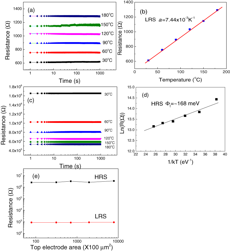
Figure 3. (a) R–Time curves of the LRS at temperatures ranging from room temperature (30 °C) to 180 °C. (b) The temperature dependence of the LRS resistance. The solid line represents the linear fit. (c) R–Time curves of the HRS at temperatures ranging from 30 °C to 180 °C. (d) Arrhenius plot of the resistance temperature data in the HRS. (e) Electrode area dependence of the HRS and LRS. Here, RHRS and RLRS are extracted at 1 V.
Download figure:
Standard image High-resolution imageIn most interface dominated resistance switching, the resistance of ON and OFF states changes inversely with the electrode area due to the lateral conduction at interface [20]. In our case, however, the HRS and LRS resistance is independent of the electrode area, as shown in figure 3(d). Since the oxygen ions are not able to migrate absolutely homogeneously, the resistance is less dependent on the whole area and the conducting region occurs locally. It suggests that the resistance switching in ITO/Eu2O3/FTO devices involves inhomogeneous conducting filaments.
It has been reported that the low electroforming field for the NiO film is associated with the presence of metallic Ni [21]. Teixeira et al [22] reported that the existence of metallic paths across the barrier was essential for the observation of 'forming-free' RS behaviour in MgO-based tunnel junctions. Xu et al [23] demonstrated that the forming-free characteristic in the TiN/ZnO/Pt structure device is attributed to more oxygen vacancies pre-existing in the ZnO film. On the other hand, Cao et al [24] indicated that the forming-free behaviour in the RS film is associated with the deposition process and internal microstructure. To realize the reason for the forming-free RS behaviour in the ITO/Eu2O3/FTO structure, XPS was performed on the Eu2O3 films. Following the trivalent europium ions configuration peak at 1136.7 eV, metallic Eu0 configuration peak at 1133.8 eV was observed clearly [25], which implies the possibility of metal Eu's existence. In figure 4(b), the O 1s signal comprised two peaks: one peak represents the Eu–O bond (located at 529.4 eV) and another peak represents the sub-oxides with Eu (located at 532.0 eV). XPS analyses have shown that the metallic europium and oxygen vacancies pre-exist in the Eu2O3 film. To further clarify the composition of the Eu2O3 films, a high-resolution TEM image and SAED have been employed and are shown in figure 4(c). Metallic Eu can be found to exist in the polycrystalline Eu2O3 films. The ring electron diffraction pattern in the inset of figure 4(c) also indicates that the Eu2O3 films are polycrystalline structure, containing many crystalline grains. A large number of crystal defects pre-existing in the Eu2O3 film during the deposition process could contribute to the formation of the conducting filaments without the electroforming process. It was reported that the electrically formed oxygen-rich interfacial layer at the IrOx/high-kx and W/TaOx interface could improve switching characteristics [13, 26]. The formation of conductive filaments should be attributed to the localized agglomeration of the oxygen vacancies in the Eu2O3 film, by analogy with the metallic europium ion [27], as shown in figure 5. We present a microscopic view for the RS behaviour in the Eu2O3 film based on the model of the filament formation and rupture mechanism. The switching phenomenon is believed to be due to oxygen vacancies and ions through nano-ionic transport and a redox process, and this can be called valance change memory (VCM) [28]. As suggested previously, an intrinsic Schottky barrier exists between the top electrode and the Eu2O3 layer contact while in the insulating state. The Eu2O3 easily creates anion deficiency because the oxygen anions are very active, and can move through the lattice relatively easily. This suggests that oxygen ion movement under external bias leads to the LRS to HRS or HRS to LRS. When the positive sweep voltage increases in a pristine device, the metal (M)–O bonds in high-k oxides break and the generated oxygen ions (O2−) will drift towards the top electrode, leading to a +2 oxygen vacancy, stable charge state, and two electrons to be localized on the nearby Eu atoms (see figure 5(a)). They tend to cluster in certain configurations with lower Vo–Vo interactions [29]. Considering a Eu atom in the proximity of these oxygen vacancies, the charge state of this Eu atom may convert Eu3+ to Eu2+, Eu+ or Eu0. Seo et al reported that the states formed by neutral Eu defects are placed at midgap and play an important role in the RS behaviour by charging or discharging the states [30]. When a sufficient number of O2+ ions are generated, the current suddenly increases because of the formation of a conducting filament and the device enters the SET state, as shown in figure 5(b). The current density through a conducting filament can reach a high value and might be responsible for producing the thermal energy that will activate the migration of oxygen ion at the highest resistive point or at the electrode–filament interface [31]. Under RESET operation, O2− will be repelled away from the top electrode and recombine the oxygen vacancies or oxidize the conducting filament, converting the device into a HRS. Figure 5(c) demonstrates the rupture process of the metallic filament. The recovery of the oxygen coordination of Eu atoms connected in a chain can be considered the rupture of the filament representing the HRS. We suggest that local Joule heating may assist the rupture of filaments to switch the Eu2O3 memory device from the LRS to the HRS.

Figure 4. The XPS characteristics of (a) Eu 3d and (b) O 1s for the Eu2O3 films deposited on FTO substrates. (c) Atomic TEM image of Eu2O3 crystal film. Inset in (c) shows the corresponding electron diffraction SAED pattern.
Download figure:
Standard image High-resolution image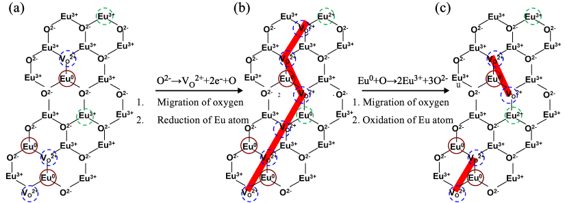
Figure 5. Schematic of the RS mechanism in Eu2O3 thin films for the (a) conduction, (b) formation and (c) rupture of filament.
Download figure:
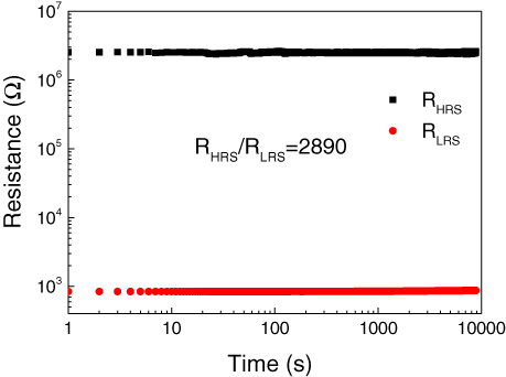
Standard image High-resolution imageIn order to evaluate the potential application in TRRAM, a reading voltage of 300 mV was applied to investigate the retention characteristics of the memory device. As shown in figure 6, the LRS and HRS were stable for more than 104 s, and no obvious degradation was observed during the tests. The statistics retention characteristics of the HRS and LRS at 300 K show a large On/Off ratio up to 2.89 × 10³. These results indicate that the ITO/Eu2O3/FTO TRRAM is highly promising as a future nonvolatile memory device.
Figure 6. Plots of retention characteristics for the HRS and LRS at room temperature.
Download figure:
Standard image High-resolution image
4. Conclusions
In this paper, we have demonstrated the RS characteristics of fully transparent high-k-rare-earth-oxide RRAM devices based on an ITO/Eu2O3/FTO sandwich structure. The conduction mechanism of the LRS for memory devices is Ohmic emission, whereas the HRS is SCL conduction and Schottky emission. The forming-free switching mechanism of the ITO/Eu2O3/FTO memory devices could be explained using a well-established formation/oxidation of oxygen-vacancy filamentary theory, which is well supported by the TEM and XPS results combing with the temperature dependence of the resistance. With the high resistance ratio, and good data retention behaviours, the fully transparent memory devices pave the way for transparent electronics and other future applications, including flexible electronic papers and smart windows.
Acknowledgments
This work has been supported by the National Science Foundation (No 60976016), the National Natural Science Foundation of China (11174135), the National 973 Project (No 0213117005), the State Key Program for Basic Research of China (No 2010CB630704), the Foundation Co-established by the Province and the Ministry of Henan University (No SBGJ090503) and China Postdoctoral Science Foundation (No 2012M511250).