

Abstract
An electro-chemical approach for controlled growth of seedless ZnO nanorods was investigated. Field emission scanning electron microscopy confirms ZnO nanorod morphology can be controlled by varying the electrodeposition duration. Increased growth time enhances the crystallinity of ZnO nanorods and releases the strain on ZnO nanorods, as revealed by x-ray diffraction analysis. A significant change in the near band gap and the defect level luminescence were observed for different growth time ZnO nanorods. The variation in zone-centre E2 (high) optical phonon mode of ZnO nanorods was studied using micro-Raman measurements. The I–V characteristics of the ZnO nanorods potentially enable applications in UV photodetection even at very low voltage range. Photodetectors based on ZnO nanorods have a faster response time (~29 s) and exhibited high photosensitivity, approximately 28 at 1 V forward bias, as compared to recent reported values. The results obtained are exciting in view of using a low cost electrodeposition technique at low temperature for achieving high-quality electrodeposited ZnO nanorods and its possible use in optoelectronic devices.
Export citation and abstract BibTeX RIS
1. Introduction
Controlled growth engineering of morphology in low dimensional ZnO structures has opened great research attention. Particularly, control of the shapes, size and morphology in the case of nanorods (NRs), nanowires, nanoribons, nanobelts with their wide range of applications viz. light-emitting diodes [1], field-effect transistors [2], sensors [3–5], solar cells [6–8], lasers [9, 10], photocatalytic systems [11, 12] and UV photodetectors [13–19] is of high interest. Special attention is focused on ZnO in the form of NRs, vertically arranged with respect to the substrate, due to their unique properties. Ordered ZnO nanostructures are expected to enhance performance of various technologically important devices. Particularly, the use of low power/energy during optoelectronic device operation is an important subject to be explored. Many methods have been employed to develop ZnO of various morphologies and size, including high temperature chemical vapor deposition (CVD) [20, 21], thermal evaporation [22], pulsed laser deposition (PLD) [23], aqueous chemical growth [4, 10], sol–gel processes [5, 24], hydrothermal [25, 26], and electrochemical methods [27–32]. However, in most of the sophisticated growth methods, the requirement of high temperature during growth restricts the choice of the substrates and further it needs costly vacuum equipment [33]. Low-cost and low-temperature fabrication methods with controllable structure and morphology of ZnO nanostructure, are still a challenge. Electrodeposition provides several advantages in comparison with other methods, like low cost, large-scale deposition and possibility of morphology control of resultant films, from rough deposits to well aligned nanorod arrays. The electrochemical synthesis of ZnO from aqueous solution containing Zn2+ ions and source of OH− consists in electro reduction of hydroxide precursor, followed by precipitation of Zn(OH)2 and formation of ZnO. A number of papers published to date have shown that the shape and the properties of nanostructures obtained may be varied by the change of parameters such as the type and concentrations of Zn and O precursors, temperature, type of a substrate and method of its pretreatment, as well as by manipulation of electrochemical parameters such as current density or electrodeposition potential. However, very few reports are available on ZnO nanorods synthesized by electrodeposition technique by varying the electrodeposition duration.
The selection of substrate also plays a very important role for the growth of vertical ZnO nanorods. A few parameters, such as lattice parameters matching and crystal structure between the ZnO nanorods and substrate, mainly affect the crystal growth behavior and quality [29]. Indium–tin-oxide (ITO)-coated glass substrate has many excellent properties, such as (i) electrical conductivity and optical transparency, (ii) high vis-NIR light transmission, (iii) uniform transmission homogeneity and (iv) reflection in the infrared range [29, 30]. The lattice mismatch is about (~3%) between the neighboring oxygen–oxygen (O–O) distance on ITO (1 1 1) and ZnO (0 0 0 1) planes [31], and O dangling bonds on the ITO layer. Hence, ITO substrate improves the initial nucleation of the ZnO and further successive growth of high-quality vertical ZnO nanorods. There is no need of a buffer or seed layer for ZnO nanorods on ITO substrate. Such structures, based on aligned ZnO nanorods on ITO substrate are very attractive for opto-electronic applications. Most of the previous research works carried out by electrodeposition methods to understand the morphology of ZnO nanorods are based on the effect of Zn+2 ion concentration in the electrolyte. Diluting the precursor solution restricts the coalescence of nanorods during deposition, hence resulting in small and uniform nanorods as reported by Shinagawa and Izaki [32]. However, precursor concentrations sometimes limit the efficiency of deposition and/or the controllability of the nanorod diameter. Moreover, stoichiometry in the sample is also an important point to resolve the problem of morphology based on concentrations.
In regards to the application using ZnO nanorods, various novel wide band-gap semiconductor nanomaterials have been explored for fabricating UV phtodetectors, such as ZnO, ZnS, SnO2, ZnSe, In2Te3, TiO2, MoS2 etc [19] using low-cost and simple technique viz. hydrothermal/solvothermal reaction, solution-based self-assembly and template-assisted growth. In spite of good progress in the field of UV photodetectors, the use of these devices in practical applications still requires an intensive effort. New techniques should be developed to improve the photosensitivity, reduce the dark current, and reduce the response time. However, one of the big challenges for the semiconductor industry is to build optoelectronic devices with high performance and low power consumption. Therefore, UV photodetectors with high photosensitivity, low dark current, and short response time with low power consumption are highly needed by society. This report establishes a low-cost, simple and unique approach to the fabrication of ZnO nanorod based UV photodetectors that can operate at very low voltage. A new strategy—that the morphological change in electrodeposited ZnO nanostructures, not only depends on the Zn+2 ion concentration but also depends on the duration of electrodeposition process—has been discussed. The effect of growth time on the morphology, structure and crystallographic form of ZnO nanorods are investigated by the techniques of field emission scanning electron microscopy (FESEM) and x-ray diffrcation (XRD) techniques. Photoluminescence (PL) and Raman measurement were performed to study the optical properties of the obtained ZnO nanorods samples.
2. Method
The electrodeposition of ZnO nanorods was performed using electrochemical cells consisting of two electrodes, one with the substrate (conducting glass ITO) as the cathode and the other a Pt sheet as the counter electrode (anode). The electrochemical cells were prepared with 0.5 mM equimolar aqueous solution of zinc nitrate (Zn(NO3)2 · 6H2O) and hexamethylenetetramine (HMT) (CH2)6N4). The growth processes, experiments and all the experimental measurements were performed under normal atmospheric conditions and the growth temperature was set at 80 °C. All solutions were prepared with deionized water purified with a Millipore Milli-Q purification system. Before electrochemical measurements, the ITO substrates were cleaned sequentially with acetone (5 min), ethanol (5 min) and deionized water. To study the effect of electrodeposition duration, the electrochemical growth of ZnO onto the ITO electrode was carried out with 5, 10 and 20 min duration time. The samples were named as S1, S2, S3 for 5, 10, and 20 min duration time respectively. The electrochemical growth of ZnO nanorods onto the ITO electrode was carried out at a fixed current density of 0.25 mA cm−2 for all the deposition. The surface morphology of the ZnO nanorods was investigated by FESEM. XRD analyses were performed on a Brucker D8 advanced diffractometer using a Cu Kα radiation source. The PL measurements were carried out at room temperature, to investigate the optical properties of the samples using a Jobin Yvon luminescence spectrometer under an excitation wavelength of 252 nm from a Hg–Xe lamp. The Raman measurements were carried out at 300 K using a Micro Raman (Jobin Yvon) instrument. I–V measurement at 300 K was carried out using a Keithley Picoammeter. Metal contacts of 1 millimeter diameter were deposited on ZnO nanorods using Indium metal wire and a micro-tip soldering iron. The distance between the two metal contacts were kept around 10 mm. The UV wavelength of 252 nm was selected for excitation by a single monochromator from the spectrum of an Hg–Xe lamp which was employed as the light source to measure the photocurrent.
3. Results and discussion
HMT, which is non-ionic and highly soluble in water, is one of the most common organic compounds added to the deposition bath to support the growth of ZnO nanorods of required morphology [25, 26]. It is known that in acidic aqueous solution at elevated temperature, HMT hydrolyses to formaldehyde and ammonia, which tends to acid-base equilibrium, according to the following equation [34]


Hence, HMT plays an important role as an additional source of OH−, which promote the nucleation as well as growth of ZnO in two dimensions. HMT is basically a nonpolar chelating agent and is attached to the nonpolar facets of the ZnO crystal, allowing growth along the [0 0 0 1] direction. As HMT decomposes at an acidic pH, we have used it as an acid source to grow ZnO nanorods by cathodic electrodeposition.
The morphology of the electrochemically grown nanorods were investigated by FESEM. Figure 1 shows the FESEM images of ZnO nanorods and the effects of the electrodeposition duration on the morphology of ZnO nanorods. Figure 1(a) shows the morphology of sample S1 where the width of the ZnO nanorods was found to vary from 25 nm to 40 nm. Similarly, figure 1(b) shows the morphology of sample S2 and the width of the ZnO nanorods varied from 70 nm to 90 nm; figure 1(c) shows the morphology of sample S3, where agglomerated nanorods with higher width (~150 nm) were observed. Figure 1(d) shows the surface morphology of a bare ITO substrate where a clean surface was observed for ITO substrate. This result suggests that, with increasing duration of electrodeposition process, the rate of growth of ZnO nanorods on ITO substrate increases.

Figure 1. FESEM images of ZnO nanorod deposited on ITO substrate at 0.25 mA cm−2 for (a) 5, (b) 10 and (c) 20 min. (d) FESEM image of bare ITO substrate.
Download figure:
Standard image High-resolution imageThis is because of the availability of more nucleation centres on the surface of the nanorods. The effect of electrodeposition duration on morphology and size is clearly visible in this set of samples. A model has been proposed to understand the ZnO nanorod growth, which is schematically represented in figure 2. In figure 2, the ZnO nanorods initially grown on ITO substrates for 5 min are represented as S1. With increasing electrodeposition time from 5 min to 10 min, the growth of ZnO nanorods continued and resulted a thicker nanorod represented as S2. Finally, increasing electrodeposition time from 10 min to 20 min, the nanorods fused together to form a structure composed of closely packed nanorods represented by S3 as shown in figure 2. In case S1, due to low deposition duration the nanorods dimensions are small compared to S2 and S3. With increasing deposition duration, the nanorods are extended radially from the centre and grow as a thick nanorod and fully cover the ITO substrate as shown in figure 1(c). Thus, the duration of electrodeposition process is a key factor in the electrodeposition of ZnO nanorods and to achieve dimensionally controlled nanorods, the time duration for the electrodeposition process definitively affects the morphology of ZnO growth.

Figure 2. Schematic representation of ZnO nanorod growth with different time durations on ITO substrate.
Download figure:
Standard image High-resolution imageTo study the effect of the electrodeposition growth time on the crystalline structure of ZnO nanorods, XRD analysis was performed on ZnO nanorods synthesized on ITO substrate at 0.25 mA cm−2 current density for different electrodeposition duration. It can be seen from figure 3, that all the three samples have peaks at 31.71, 34.36, 36.30, 47.61, 56.59, 62.86, 66.40, 67.99, 69.19, 72.73 and 76.97, corresponding to the (1 0 0), (0 0 2), (1 0 1), (1 0 2), (1 1 0), (1 0 3), (2 0 0), (1 1 2), (2 0 1), (0 0 4) and (2 0 2) planes of ZnO respectively, which correspond to the typical diffraction peaks of hexagonal wurtzite ZnO (with reference to JCPDS No. 36e1451). The presence of several peaks in the XRD reveals that the nanorods are polycrystalline. No impurity phases were observed in XRD spectra. Hence, the use of zinc nitrate and HMT precursors seems to be an effective way to grow ZnO nanorods by electro deposition technique without inducing any kind of undesired compounds. All the diffraction peaks belong to the ITO, labeled with an asterisk mark as shown in figures 3(a) and (b). However, sample S3 does not have any ITO peak as compare to sample S1 and S2 (figure 3(c)). It is to be noted that during long time duration deposition, as the nanorod grows more in its width as well as length, a coalition of many nanorods into a single wide nanorod for which there is no void or empty space available on the surface of the sample, as seen from the FESEM image of figure 1(c). Hence the increase in thickness and compactness of ZnO nanorods in sample S3, prevents the x-ray from reaching the ITO substrate during XRD measurement. Thus the absence of ITO peaks in XRD measurement is observed for sample S3.

Figure 3. XRD patterns of ZnO nanorods eletrodeposited on ITO substrate at (a) 5 (sample S1), (b) 10 (sample S2) and (c) 20 (sample S3) min duration.
Download figure:
Standard image High-resolution imageThis is important to observe the (0 0 2) peak for ZnO material because it decides the orientation, phase and disorder in crystal of the ZnO sample. Figure 4(a) shows the Gaussian fittings of the (0 0 2) peak of all three samples S1, S2 and S3 respectively. In ZnO hexagonal structure, the plane spacing is related to the lattice constants 'a' and 'c' by the following relation [30],
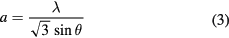
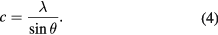

Figure 4. (a) Gaussian fittings of the (0 0 2) XRD peak of ZnO nanorods eletrodeposited on ITO substrate, (b) FWHM of the (0 0 2) peak as a function of electrodeposition duration, (c) intensity of the (0 0 2) peak as a function of electrodeposition duration (d) peak position of the (0 0 2) peak as a function of electrodeposition duration.
Download figure:
Standard image High-resolution imageThe microstrain of the ZnO nanorods samples were calculated using equation (5).
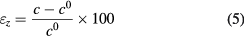
where c is the lattice constant of the ZnO nanorods calculated from the XRD measurements, and c0 = 5.206 Å is the lattice constant of the standard unstrained ZnO. The unit cell parameters 'a', 'c', and microstrain (εz) obtained from the XRD data of ZnO nanorods samples are tabulated in table 1.
Table 1. Structural parameters of the ZnO nanorods.
| Sample ZnO NRs | XRD (0 0 2) peak position | FWHM (0 0 2) peak | a (1 0 0) | c (2 0 0) | c/a | Strain ɛz (%) |
|---|---|---|---|---|---|---|
| S1 | 34.43 | 1.14 | 3.25 | 5.203 | 1.600 | −0.05 |
| S2 | 34.42 | 0.90 | 3.25 | 5.204 | 1.601 | 0.03 |
| S3 | 34.40 | 0.36 | 3.25 | 5.207 | 1.602 | 0.01 |
The full-width-at-half-maximum (FWHM) values of the (0 0 2) peak of ZnO nanorods samples on ITO substrate are found to be 1.142 47, 0.904 23 and 0.369 11 for S1, S2 and S3 respectively. These results suggest that as the growth time increases the FWHM value of (0 0 2) peak decreases as shown in figure 4(b). As the time of deposition increases, the crystallinity of the ZnO nanorods improves. The reasonably narrow FWHM widths for sample S3 demonstrate the high crystal quality of ZnO sample obtained by electrochemical deposition on ITO substrates. Similarly, as the deposition time increases, the crystallinity is improved, hence the peak intensity becomes large. As shown in figure 4(c) the (0 0 2) peak intensity increases with increasing deposition duration, again establishing better crystallinity for long duration deposited samples. Previous researchers show similar kinds of results in ZnO nanorods prepared by electrodeposition technique [35]. The intensity of (0 0 2) plane for ZnO nanorods is more pronounced in the case of sample S3 than that of sample S1, establishing that the low electrodeposition duration samples induces more crystallographic defects and hence degrades the crystal quality. As shown in figure 4(d), the (0 0 2) peak positions have a slight shift towards lower angles, generating a compressive strain on the nanorod samples. Usually, nanostructured materials are always strained because of large numbers of grain boundaries and associated distance between them. The shift in (0 0 2) peak position could be due to the intrinsic microstrain [30] and the strain releasing upon increasing time of deposition as shown in figure 4(d). In general, a change in d-spacing is to be observed in nano-materials, which is attributed to the change in lattice parameters at nanometre scales due to enhanced surface forces. For example, the lattice parameter c of bulk ZnO is about 5.206, and the lattice parameter c of samples S1, S2 and S3 are 5.203, 5.204 and 5.207 respectively. These values suggest that there is a change in lattice parameter with reference to bulk ZnO. The change in lattice parameter is due to microstrain developed during growth. The enhancement in surface forces generates a microstrain/stress on the sample. In the case of sample S1 the dimensions of nanorods are comparatively less than in sample S2 and S3. Similarly, sample S2's dimensions are comparatively less than those of sample S3. This suggests that lowering the size of the nanorods increases the strains, which can be seen from table 1. As seen from table 1 the S1 sample is more strained than S2 and S3, which confirms that increase in size of the nanorods releases the strain. A minimum tensile strain of (0.01%) is observed in case of sample S3. All the results indicate that an increase in growth time improves the crystallinity of ZnO.
PL measurement can provide information related to deep level traps in ZnO nanorods. It is well known that UV PL is related to the band edge emission while visible PL is due to defects in the material. As shown in figure 5, the PL spectra of all three ZnO nanorods samples consists of a broad and intense near band edge peak and a visible luminescence peak at room temperature. A usual characteristic of this near band edge PL band is broadening towards the Stokes part of the emission. Several mechanisms have been proposed for the broadening of this PL band [36–38]. It has been observed that the direct transition of electrons from the conduction band tails to valence band tails is the reason for this PL broadening. Moreover, the broadening of the PL band also due to potential fluctuations induced by the high concentration of intrinsic defects or impurities. The possible nature of the near band gap and defect related PL band in electrodeposited ZnO nanorods samples will be discussed here.

Figure 5. PL spectra of ZnO nanorod samples (S1, S2 and S3) synthetized at different electrodeposition durations.
Download figure:
Standard image High-resolution imageAs shown in figure 5, the Gaussian fitting shows the detailed analysis of the band-edge region and visible region of PL features of the ZnO nanorods sample grown on ITO. According to the previous studies [37] the band-edge PL of bulk ZnO material can be divided into seven parts: (i) free excitons (FE: 355 nm to 367.2 nm); (ii) excitons bound to ionized donors (D + X: 367.2 nm to 368.5 nm); (iii) excitons bound to neutral donors (D0X: 368.5 nm to 368.95 nm); (iv) excitons bound to neutral acceptors (A0X: 368.95 nm to 369.7 nm); (v) exciton complexes with deep centers (369.7 nm–372.0 nm); (vi) two-electron transitions (372 nm to 374 nm); and (vii) phonon replica region (374 nm). Comparing these values of different near band edge region emissions with ZnO nanorods samples, the weak PL peak 1 in figure 5 lies in the free exciton region with a maximum at around 365 nm for all three samples. It is to be noted that the origin of the UV PL, in the range of 360–420 nm, from ZnO is generally attributed to the photo-stimulated creation of excitons having energies just below the ZnO band-edge and their subsequent recombination. Hence the strong PL peak 2 around 385 nm in figure 5 is a near band edge luminescence observed by photo-stimulated excitons observed in all three ZnO nanorods samples. All the studied samples show PL in the visible region between 450 and 650 nm, as shown in figure 5. This broad band can be related to the presence of defects-related states consisting of a green component centered at around 519 nm (peak 3) and a yellow component at around 530–590 nm (peak 4). According to the literature, the broad band luminescence in visible range, extending over a range, is an overlap of several peaks related to defects in the ZnO structure such as zinc and oxygen vacancies and/or interstitials [38]. The visible region PL process is generally understood to be the recombination of a hole with an electron associated with an oxygen vacancy in ZnO [38]. Therefore, the near band bandgap emission including an emission from free exciton was detected in the spectra of all three samples. Although UV emission is quite rare in the case of electrodeposited ZnO samples, the presence of free exciton PL band in this case is an exception.
Figure 6 is the Raman spectra of ZnO nanorods samples S1, S2 and S3 under different electrodeposition duration. It can be seen that the Raman spectra exhibit the main peak located at 437 cm−1. The peak at 437 cm−1 was attributed to the optical phonon E2 (high) of the ZnO, and it belongs to the characteristic Raman active peak for the wurtzite hexagonal phase of ZnO [29]. Mainly, 439 cm−1 corresponds to E2 (high) of the bulk ZnO [31]. Around 2 cm−1 shift is observed in case of ZnO nanorods samples. The phonon uncertainty obeys the rule ▵q ~ 1/d, where d is the diameter of the nanostructures. The 2 cm−1 shift is due to the spatial confinement inside nanostructures giving rise to a redshift and asymmetric broadening of the Raman peaks in nanostructures compared to bulk crystals [39]. Similarly, the intensity of peaks at E2 (high) increases with increasing electrodeposition duration, which means crystallinity of nanorods is improved. Indeed, we have found that in the case of thick nanorods grown on ITO (sample S3), the structural quality was markedly improved as discussed in the previous section. This analysis was supported by the result of the XRD characterization shown in figure 3. The peak positions of the optical phonon modes were in good agreement with the results reported by other literature [29, 39]. The FWHM of the peak corresponding to optical phonon E2 mode, was found to be 19 cm−1, 18 cm−1 and 12 cm−1 for sample S1, S2 and S3 respectively. The narrower FWHM of E2 (high) peak of S3 sample, indicates that the crystal quality is better compared to sample S1 and S2.

Figure 6. Raman spectra of ZnO nanorod samples (S1, S2 and S3) synthetized in different electrodeposition time periods.
Download figure:
Standard image High-resolution imageFigure 7 shows the typical I–V characteristics of electrodeposited ZnO samples (S3) measured in the dark and under UV illumination. Assessment of the photosensitivity of ZnO nanorod samples was carried out using a two probe point contact method. Two indium contacts were formed on top of the ZnO nanorods for electrical measurement as shown in the inset I of the figure 7. A good ohmic contact was confirmed between the ZnO nanorod sample and the Indium metal. A linear curve under both forward and reverse bias was obtained in dark and under UV illumination for the ZnO nanorod samples electrodeposited on ITO substrate. The dark current for a bias voltage of 1 V was found to be 0.8 µA. The photocurrent upon exposure to UV illumination is remarkably enhanced to 25 µA at 1 V bias, which is significantly higher than the dark current, and represents more than 30 times enhancement at 1 V forward bias. Although sample S1 and S2 show similar behavior in their I–V characteristic (figure not shown here), the enhancement in photo-current is very high in the case of sample S3. The mechanism responsible for the enhancement of photocurrent in sample S3, as compared to sample S1 and S2 can be understood as follows. As observed from the morphology of samples S1 and S2 (FESEM figure 1), they have smaller dimensions with respect to S3, thus have higher surface-to-volume ratio, which increases the surface trap states. Free electrons are captured by these surface states, reducing the free electron density in the samples. This reduction in electron density is greater for samples S1, S2 and less for sample, S3. For this reason, samples S1 and S2 show less photo-current as compared to sample, S3. The higher free electron density along with comparatively high surface to volume ratio in sample S3, provides efficient absorption sites of oxygen molecules. During the photodetection process, the oxygen molecules are adsorbed at the ZnO nanorods surface to create charged ions by capturing free electrons from the ZnO:


Figure 7. (a) Dark and UV light illuminated I–V characteristics of ZnO nanorod sample (S3), electrodeposited on ITO substrate, (b) photosensitivity factor as a function of bias voltage for ZnO nanorod sample (S3), (c) time dependent photoresponse at a bias voltage of 1 V for ZnO nanorod sample (S3).
Download figure:
Standard image High-resolution image
In this process, a depletion region is formed near the surface, which results in a decrease of the conductivity of ZnO nanorods. As the ZnO nanorods are illuminated with UV light having photon energy more than the band gap, electron–hole pairs are generated:

The holes recombine with trapped electrons, which are already captured by the oxygen molecules:

Hence, there is an increase in carrier concentration and increase of the ZnO nanorods conductivity [40–42]. This result clearly demonstrates that the size and surface morphology of ZnO nanorods play an important role in their transport behavior.
Photosensitivity is one of the most important characters for photosensitive materials, which is defined as [42]:

where Id is the dark current and Ip is the photo current. Figure 7(b) shows the photosensitivity characteristics of the ZnO nanorods as a function of applied bias at room temperature. ZnO nanorods (sample S3), exhibited the highest photosensitivity of 28 at applied bias of 1 V when excited by the UV light. Remarkably, the photosensitivity is observed more than 18 at as low as 0.1 V forward bias voltage. This result is better compared with one of the recent reported values of photosensitivity factor from ZnO-material-based films available in the literature [42, 43], where they reported 1.62–3.085-fold improved photosensitivity factor at the bias voltage of 2 V.
Figure 7(c) shows the most important features of a photodetector, i.e. the speed of its response and the recovery time. The response time and the recovery time of the ZnO nanorods (sample S3) under UV illumination were found to be 29 and 49 s respectively. Most of the published results show different response times ranging from few nanoseconds to minutes [42, 44]. It is to be noted that electron–hole generation is a fast process for which a high photo current is produced in a very short time. In this case the response time is 29 s for 1 V bias supply. Then during the re-adsorption process, it slowly reached the steady-state of photo current value. As the adsorption and photo-desorption processes are slow processes [44], the photo current reaches the saturation value very slowly for which the recovery time is 49 s in this case. It is also known that the adsorption process is slower than the photo-desorption process. Therefore, during UV illumination, few holes are left after recombination with the electrons present in the ionized oxygen and available for recombination with the exciton-related free electrons [44]. During photocurrent decay, the exciton related electron–hole recombination dominates, which corresponds to the faster decay component in the photocurrent, so at the start, the photocurrent decreases very rapidly; then with the surface re-adsorption of oxygen due to free electrons on the surface, the photocurrent returns to its original value very slowly. In a similar manner, the photocurrent of sample S3, reached the saturation value very fast and the decay process was very slow as shown in figure 7(c).
There are several reports [13–19] on UV photodetectors satisfying the photodetector characteristic on response speed, selectivity, and sensitivity. Chen et al [13] in one of their review report, show a SnO2 nanonet could show four-fold enhancement in photocurrent with respect to its dark current whereas the present study (ZnO nanorods sample S3), shows more than thirty-fold enhancement in its photocurrent with respect to its dark current at 1 V bias. Moreover, the dark current in their case is still high for the purpose of a suitable device. Similarly, a single-layer MoS2 photodetector, proposed by Lopez-Sanchez et al [45] showed a fast response speed where the rise and decay times are 4 and 9 s respectively, but the device is limited to visible light detection only. Pandey et al [42] and Zhou et al [43] recently reported a UV photodetrector based on ZnO nanomaterials, which showed a similar response speed to the present device but the sensitivity of their device is very low in comparison to the present device. Therefore, the electrodeposited ZnO nanorods, showing significant UV photocurrent generation and high photosensitivity at low voltage ranges, can be a potential candidate for a low-cost prototype UV photo-detector.
4. Conclusions
In summary, controllable growth of ZnO nanorods is possible using electrodeposition techniques by varying the growth duration. The structural, morphological and optical properties of ZnO nanorods fabricated by varying the deposition duration in using an electrochemical deposition technique have been investigated. The FESEM studies showed that ZnO nanorods morphology can be tuned by varying the electrodeposition duration. The structural analysis has confirmed the improvements in crystallinity during higher duration growth period of ZnO nanorods. The resulting ZnO nanorods exhibited strong UV emission as well as a broad visible emission. The Raman spectra reveal the optical phonon mode corresponding to E2-high with narrow FWHM confirms the high quality of ZnO nanorods. The results obtained in this study demonstrate that the structure, morphology and optical properties of electrodeposited ZnO nanorods can be tailored by tuning the electrodeposition duration without using any catalyst, additives, seed layer or post heat treatment. The heterojunction In/ZnO nanorods/ITO structure shows a remarkable response to UV light at room temperature. As compared with the earlier report, ZnO nanorods in this study exhibited the highest photosensitivity of 28.0, at bias voltage at 1 V when excited by the UV light of wavelength 252 nm. The response time of the device reported here is better than that of polycrystalline ZnO based photodetectors reported earlier. This result suggests that ZnO nanorods on ITO substrate can be explored for opto-electronic device applications.
Acknowledgments
The author would like to thank Prof S N Sahu (deceased), Ex-Professor, Institute of Physics, Sachivalaya Marg, Bhubaneswar-5, India and Prof S Nozaki, University of Electro-Communications, Chofugaoka, Chofu Shi, 182-8585 Tokyo, for their helpful discussions and use of the experimental facilities.