
Abstract
Oxide electronic materials provide a plethora of possible applications and offer ample opportunity for scientists to probe into some of the exciting and intriguing phenomena exhibited by oxide systems and oxide interfaces. In addition to the already diverse spectrum of properties, the nanoscale form of oxides provides a new dimension of hitherto unknown phenomena due to the increased surface-to-volume ratio.
Oxide electronic materials are becoming increasingly important in a wide range of applications including transparent electronics, optoelectronics, magnetoelectronics, photonics, spintronics, thermoelectrics, piezoelectrics, power harvesting, hydrogen storage and environmental waste management. Synthesis and fabrication of these materials, as well as processing into particular device structures to suit a specific application is still a challenge. Further, characterization of these materials to understand the tunability of their properties and the novel properties that evolve due to their nanostructured nature is another facet of the challenge. The research related to the oxide electronic field is at an impressionable stage, and this has motivated us to contribute with a roadmap on 'oxide electronic materials and oxide interfaces'.
This roadmap envisages the potential applications of oxide materials in cutting edge technologies and focuses on the necessary advances required to implement these materials, including both conventional and novel techniques for the synthesis, characterization, processing and fabrication of nanostructured oxides and oxide-based devices. The contents of this roadmap will highlight the functional and correlated properties of oxides in bulk, nano, thin film, multilayer and heterostructure forms, as well as the theoretical considerations behind both present and future applications in many technologically important areas as pointed out by Venkatesan.
The contributions in this roadmap span several thematic groups which are represented by the following authors: novel field effect transistors and bipolar devices by Fortunato, Grundmann, Boschker, Rao, and Rogers; energy conversion and saving by Zaban, Weidenkaff, and Murakami; new opportunities of photonics by Fompeyrine, and Zuniga-Perez; multiferroic materials including novel phenomena by Ramesh, Spaldin, Mertig, Lorenz, Srinivasan, and Prellier; and concepts for topological oxide electronics by Kawasaki, Pentcheva, and Gegenwart. Finally, Miletto Granozio presents the European action 'towards oxide-based electronics' which develops an oxide electronics roadmap with emphasis on future nonvolatile memories and the required technologies.
In summary, we do hope that this oxide roadmap appears as an interesting up-to-date snapshot on one of the most exciting and active areas of solid state physics, materials science, and chemistry, which even after many years of very successful development shows in short intervals novel insights and achievements.
Guest editors: M S Ramachandra Rao and Michael Lorenz
Export citation and abstract BibTeX RIS

Original content from this work may be used under the terms of the Creative Commons Attribution 3.0 licence. Any further distribution of this work must maintain attribution to the author(s) and the title of the work, journal citation and DOI.
1. Oxide films and heterostructures for electronics, memory, magnetics, photonics, energy and health
T Venkatesan
National University of Singapore, Singapore
Status.
Since the invention of the pulsed laser deposition (PLD) process and the advent of high Tc superconductivity [1] in the 1987 time frame, the field of oxides has accelerated at an extraordinary pace with potential impact on numerous fields. I will highlight some of the key driving contributions of oxides in each area of interest and also point out what is needed to make significant progress.
Current and future challenges.
Electronics.
From the perspective of electronic devices one of the key issues is achieving higher mobility for carriers in oxides and the transport in most oxides is determined by the overlap of the cationic and anionic orbital. In the case of TiO2 this is the Ti 3d and oxygen 2p overlap which is very sensitive to the O–Ti–O bond angle. The results were clearly demonstrated for 2D electron transport in the TiO2 system where the maximum metallic behaviour is seen for the case of TiO2 on SrTiO3 (where the bond angles are 180 degrees), weak localization in the case of anatase TiO2 (153 degrees) and strong localization in the case of rutile TiO2 (81 and 93 degrees). Unlike conventional metals where molecular orbitals do not directly affect transport except indirectly via phonons, in the case of oxides they are very important and give us a way to engineer the carrier mobility by tuning this overlap via, strain, doping etc [2]. From a fundamental perspective this system is a good example where electron-polaron interactions can be well studied. By minimizing the strain at the surface of SrTiO3 mobility in excess of 100 000 cm2 V−1 s−1 has been achieved at low temperatures [3].
Memory.
In tunnel junction memories integrating ferroelectrics with conventional tunnel junctions may give us much lower switching energies with practical ON/OFF ratios. Recent work on ferroelectric tunnel junctions shows that the ON/OFF ratio can be enhanced significantly by increasing the number of interfaces in addition to the FE tunnel barrier [4]. The switch ON and OFF characteristics are determined by the ferroelectric only and while the ON/OFF ratio increases with number of barriers it also causes an increase in the ON state resistance which is not desirable. FE tunnel barriers as thin as two unit cells can switch while the ON state resistance can be made comparable to today's commercial MTJs. An order of magnitude reduction in the FE coercive fields are necessary to make this a competitive, low energy consuming memory technology.
Photonics.
Ferroelectrics on silicon enable the making of wide band width optical modulators that can work at a variety of optical wavelength and speeds approaching 40MB s−1 [5]. These devices have the potential for 100 MB s−1 modulation speeds but the best devices today have only been demonstrated on MgO. Such all wavelength modulators would compete against established technologies such as ones based on LiNbO3 (handicapped by large sizes) or the III–V semiconductors (wavelength specific due to electro absorption modulation mechanism). For commercial applications these oxide based devices need to be built on a silicon platform where high quality electro-optic (ferroelectric) layers need to be deposited with suitable buffer layers to preserve the high crystalline quality of the over layers. In order to achieve mode confinement the low index buffer layer needs to have a thickness of at least 200 nm. A scalable process for the fabrication of such oxide heterostructure layers for large areas does not exist today and there is a clear need for this.
Magnetics.
Oxide magnetism received a significant boost with the advent of high temperature superconductors followed by a resurgence of interest in colossal magneto-resistive manganites followed closely by diluted magnetic semiconducting oxides. While the origin of magnetism in these systems was not fully understood, the notion of defect mediated magnetism in oxides was advanced by Sawatzky et al [6]. The first such demonstration was in TiO2 observed with Ta substitution at the Ti site. Spectroscopic analysis clearly established titanium vacancies as the primary source of magnetism with the donor electrons from Ta substitution being responsible for the magnetic exchange [7]. The observed magnetism was weak as the concentration of Ti vacancies was below 1021 cm−3 and stability consideration would dictate the difficulty of producing higher levels of sustainable defects leading a limit on the strength of magnetism possible via such an approach. However, extremely novel magnetic exchange is possible in oxide systems mediated by polar layers and the exact mechanism of the exchange which involves spin-orbit interactions is not fully understood but holds promise for novel magnetic devices utilizing magnetic exchange [8].
Energy.
A number of oxides have been strong candidates in catalysis applications and owing to their stability in harsh chemical environments and reasonable band match with reaction pathways, materials such as Fe2O3 and TiO2 have been popular. However, recently a water splitting metallic oxide was introduced which seems to have fascinating properties [9]. Besides being a conductor, this material is an efficient water splitter and the mechanism of the optical absorption, carrier decay have been now clearly understood. It turns out that this family of materials MNbO3 (M = Sr, Ca, Ba) is a degenerate wide bandgap semiconductor with a bandgap of over 4 eV but an electronic carrier density of over 1022 cm−3, an order of magnitude short of elemental metals [10]! The optical absorption in the material occurs through a plasmonic absorption at 1.9 eV arising from the large carrier density and the hot carrier lifetime after plasmonic excitation is very long (>250 ps) which explains the efficiency of these materials in water splitting. Such a strongly correlated electronic material promises a novel approach in the design of catalysts.
Health.
Oxide surfaces show a strong chemistry dependence on bio processes such as bio film formation, cell growth and cell differentiation. The origin of this behavior has to do most likely with the adhesion of macromolecules such as extracellular matrix proteins or lipids on specific surfaces where these molecules exhibit adherence. In addition, surface chemistry can also play an enhancing or inhibitory role in the cellular proliferation process. Oxides such as Y2O3 show significant lack of adhesion for cells such as fetal fibroblasts compared to ZrO2 surfaces [11]. A comparable behavior was also seen for keratinocytes and neuronal stem cells. In the case of stem cells the proliferation after differentiation was doubled over ZrO2 surfaces in comparison with standard glass (or plastic) surfaces. With the large number of oxide surfaces available this field is likely to expand rapidly in the near future. The applications are numerous including coatings for implants, cell localization on surfaces and also for antibacterial coatings and for harvesting drug resistant bacteria for development of antibiotics for so called super bugs.
Advances in science and technology to meet challenges.
Large area deposition of high quality crystalline oxides to preserve their functionality is of extremely important for the commercial applications of the developments in this material. Another major challenge for the proliferation of oxide electronic devices is the compatibility with silicon technology. Growth of high quality functional oxides on silicon with a minimal native oxide barrier on the surface of silicon will be a key requirement. High aspect ratio patterning techniques (similar to reactive ion etching) need to be developed. For biological applications a low cost method that results in highly adherent, stoichiometric coatings as well as a highly repellent coatings would be of value.
Concluding Remarks.
The field of oxides is reaching an interesting stage where potential large commercial applications are emerging and the challenges are in the deposition and processing of the materials and the success of this technology rests on how well these challenges are overcome.
2. Is the new oxide electronics (r)evolution solution based?
E Fortunato1, P Barquinha1, R Branquinho1, D Salgueiro1, E Carlos1, A Liu2, F K Shan2, and R Martins1
1 i3N/CENIMAT, Department of Materials Science from Faculty of Science and Technology, Universidade NOVA de Lisboa and CEMOP/UNINOVA, Campus de Caparica, 2829-516 Caparica, Portugal
2 College of Physics and Lab of New Fiber Materials and Modern Textile, Growing Base for State Key Laboratory, Qingdao University, Qingdao 266071, China
Status.
The evolution from rigid silicon-based electronics to flexible electronics requires the use of new materials with novel functionalities that allow non-conventional, low-cost and environmental friendly processing technologies. Among the alternatives, metal oxide semiconductors have brought to attention as backplane materials for the next generation of flat panel displays [12]. After the huge success and revolution of transparent electronics and with the worldwide interest in displays where metal oxide thin films (MOTF) have proved to be truly semiconductors, display backplanes have already gone commercial in a very short period of time, due to the huge investment of several high profile companies: Sharp, Samsung, LG, BOE [13]. These materials have demonstrated exceptional electronic performance as active semiconductor components and can be tuned for applications where high transparency/electrical conductivity is demanded and the global market for transparent electronics is expected to grow to nearly $7.1 billion by 2018, as it was stated by several forecast agencies [14].
In terms of the actual thin-film transistor (TFT) technology, In–Ga–Zn–O (IGZO) has been in mass-production since 2012. The main advantages of IGZO based TFTs are: high resolution, lower leakage current, less power consumption and less noise influence. Although IGZO technology is currently strongly targeted for active-matrix liquid crystal display (AMLCD) and active-matrix organic light emitting diode (AMOLED) applications, IGZO is proved to be a better semiconductor platform than a-Si:H for migrating towards other platforms like: photodetectors; memories; x-ray sensors and biosensors. In order to better visualize the main advantages of this technology in display applications, the merits of IGZO system are highlighted in figure 1.

Figure 1. The IGZO TFTs own more pixel per area and thinner wiring than current a-Si:H TFTs, resulting in a higher display resolution; The IGZO mobility is higher and the leakage current vastly lower. The on/off ratio is phenomenal >109. Low leakage current, combined with smaller size, makes it a clear winner for smart phones and tablets.
Download figure:
Standard image High-resolution imageCurrent and future challenges.
The current fabrication techniques require high vacuum and photolithographic processes that are expensive and keep production at high costs or similar to those of a-Si:H. Solution based fabrication methods have been pursued as an alternative for economically viable large-scale electronics [15]. The cost can be lowered by 64% since solution-based processes do not require vacuum, gases and lithography [16]. Consequently the developments of the solution-based processes that can be used with low temperature techniques are highly desirable, such as self-combustion synthesis, water-inducement (WI) route, and deep-ultraviolet (DUV) photochemical activation, etc. Among these, WI route makes significant contributions and its popularity is expected to increase with years. The WI system is only composed of metal nitrates and deionized water, which is considered to be healthier and environmental friendlier [17, 18]. In addition, the WI route has been proved to be compatible with various film fabrication techniques, such as spin coating, spray pyrolysis, or printing.
Most MOTF semiconductors reported are based on ZnO and In2O3 and combinations of these oxides such as In-Zn-O (IZO) or IGZO [19, 20]. Alternative semiconductor materials that rely on abundant and non-toxic elements such as zinc tin oxide (ZTO) are being explored as a In and Ga free alternative showing promising results [21]. The current trend is the use of non-critical (sustainable) oxide semiconductor materials combined with low cost and low temperature deposition systems. Recently, following these recommendations there has been remarkable development in solution processed inorganic MOTF semiconductor materials for high-performance TFTs without using critical raw materials. Comparing the evolution of the annealing temperature of MOTF by solution process we can observe a decrease of nearly 500 °C in the last eight years, reaching in some cases values comparable to the ones produced by physical techniques, as can be seen in figure 2.
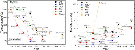
Figure 2. Left graph: evolution of the annealing/processing temperature of solution based TFTs over the last 10 years. We have plotted only TFTs presenting device mobility higher than 1 cm2 V−1 s−1. Right graph: evolution of device mobility of solution based TFTs over the last 10 years [22–56]. Due to the high number of references (>500), we have plotted only the highest values reported for device mobility. All the data will be available soon in a review paper.
Download figure:
Standard image High-resolution imageAdvances in science and technology to meet challenges.
The rapid advances of n-type oxide semiconductors such as IGZO, ZTO, ZnO and In2O3 are pushing forward the realization of high-performance oxide TFTs. The missing key ingredient for the development of next-generation transparent electronics is their hole-transporting (p-type) counterparts with comparable performance, since the p-type is thought to be better suited for conventional OLED pixels and will enable the development of the strongly desired complementary metal-oxide-semiconductor (CMOS) circuits. To date, only a few p-type MOTF (i.e. CuxO, SnO, and NiO) were reported and incorporated into transistors as p-type channel. Unfortunately, their electrical properties and fabrication techniques are not yet good enough for practical applications, necessitating further studies. For this reason, future attention should concentrate on the development of high-performance p-type TFTs, especially using low-cost solution process, and explore their applications in advanced displays and all-oxide CMOS electronics.
Concluding remarks.
Multicomponent MOTF are leading the next generation of high performance materials for a wide range of applications. Transparent electronics is currently approaching its third generation, revealing to be a very promising technology. MOTF processing by physical vapour deposition (PVD) techniques like rf magnetron sputtering has been well established and has demonstrated high performance devices, however these require complex high vacuum equipment which is a major drawback, especially if we are targeting low cost applications. In contrast, the solution process has many advantages such as large-area deposition, roll-to-roll capability, easy control of composition, atmospheric processing, and low cost. The new paradigm of transparent electronics has attracted much interest as a novel technical solution in the field of the next generation of consumer electronics. The ultimate goal of this 'see-through' device is to realize an integrated system equipped with ubiquitous functions of information storage, image display and networking, which strongly demands an embeddable transparent array of non-volatile memory.
3. Bipolar oxide devices
Marius Grundmann
Universität Leipzig, Institut für Experimentelle Physik II, Linnéstr. 5, D-04103 Leipzig
Status.
The majority of oxides are unipolar materials, i.e. they exist only either as n-type or as p-type material. Only a few oxides such as SnO are known to entertain n- and p-type conductivity. The difficulties of finding a reproducible and stable process for the p-doping of ZnO are well known. Therefore presently, devices based on oxides are mostly unipolar. The most prominent materials for application are TCOs (transparent conductive oxides) for transparent, highly conductive (ohmic) contacts [57]; these materials, such as ZnO:Ga and SnO2:F, are n-type due to the much superior mobility compared to transparent p-type oxides. Using oxide semiconductors, high rectification diodes have been built with Schottky (metal–semiconductor) contacts to various oxides such as ZnO or Ga2O3, also allowing the fabrication of high efficiency photodetectors [58]. Amorphous InGaZnO is used as channel material in thin film transistors offering significant higher performance (mobility >10 cm2 V−1 s−1) than a-Si (µ < 1 cm2 V−1 s−1) [59], commercialized nowadays in TFT displays.
While the rectification of bipolar (p–n) diodes based on oxides has idled for the last twenty years at low values not surpassing 103, recently high rectification (>1010) oxide p–n diodes were reported by us, namely based on ZnO/ZnCo2O4 (ZnO/ZCO) [60] and ZnO/NiO [61] (figure 3). Also highly rectifying (>109) completely transparent ZnO/CuI diodes have been reported [62]. A review has been recently published [63]. Thus the path has been opened for high performance bipolar oxide devices such as photodetectors, solar cells, sensors, transistors (junction field effect transistor, JFET) [63, 64] and integrated circuits based on them. While crystalline materials generally are expected to provide the highest performance, amorphous materials allow advantages in fabrication (room temperature processing, low energy budget, roll-to-roll deposition, amorphous substrates) and applications (large area devices, flexible electronics). The said ZnO/ZnCo2O4 and ZnO/NiO diodes already contain a room temperature deposited p-type oxide and transistors have been built with these materials [64, 65]. Also fully amorphous bipolar oxide diodes based on ZTO/ZCO (ZTO: zinc-tin-oxide) with a rectification >106 and ideality factor close to 1 have been reported [66] (figure 3). Bipolar devices in principle offer advantages such as low reverse current, low voltage operation and ease of fabrication.
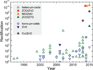
Figure 3. Rectification of various oxide homo- and heterojunction diodes versus the year of publication. Filled symbols represent results from our laboratory. Reprinted with permission from [63].
Download figure:
Standard image High-resolution imageCurrent and future challenges.
Still there are some basic things that need to be understood regarding the physical mechanisms present in bipolar oxide heterostructure diodes. For type-II band lineup, the transport mechanism has been found to be interface recombination [61]; this limits the ideality factor to values around two. The interface recombination velocity, however, will depend on interface properties and fabrication details. Both fast and slow interface recombination can have their merits for devices. Type-I band lineups and also type-III interfaces ('broken gap', e.g. for CdO/NiO [63]) need to be studied in more detail regarding the relative importance of thermionic, tunnel and recombination currents and their design and control.
Generally, p-type oxides suffer from low mobility, often due to large hole mass or hopping transport mechanisms. But also higher mobility n-type materials (towards and beyond 100 cm2 V−1 s−1) are desirable for higher speed or energy efficient devices. Additional properties such as transparency (using wide gap oxides, limiting mid-gap absorption) and mechanical flexibility (using amorphous oxides) need to be fully explored. Also there is a drive to avoid rare, expensive and toxic metals, indium being one of them.
While so far mostly diodes and a few transistors have been demonstrated, higher integrated circuits are the ultimate goal, requiring reproducibility and stability. Initial results are very promising for certain materials [60], but surely much more work is needed in this direction. A big challenge is the transfer of the CMOS concept to oxide devices. The combination of n-type and p-type channels is a formidable task which so far has not led to devices superior to those achieved with unipolar concepts, mostly due to the low performance of the p-type oxides. Besides electronics, also photovoltaics has become interesting and wide gap oxides allow for invisible energy sources [67].
As a fabrication method, magnetron sputtering seems the method of choice since it is generally an established industrial process and allows large area fabrication and roll-to-roll processing. Wet chemical processes and printing so far had very little impact on the fabrication of bipolar oxide devices, however, further progress in this direction may make them interesting also for industrial scale production.
Advances in science and technology to meet challenges.
A key to the device performance of bipolar (but also unipolar) devices is the improvement of mobility. While possibly a limit seems to have been reached for improving multi-cation oxides, multi-anion (n-type) oxides offer a possible solution. One of the promising materials is ZnON [68]; more such compounds should be searched for and investigated as channel materials and as part of p–n structures. The control of carrier density and its temperature and long-term stability in any of these materials remains a prime issue; often defects are the source of carriers while generally impurity doping is less important or impossible.
The fabrication and control of the p–n interfaces is a challenge and must be combined and transferred to large area and fast fabrication technologies such as sputtering. Many more hetero-structure combinations have to be tested and the promising ones systematically improved. A focus should be on the use of low toxicity, readily available cations (Zn, Sn, Cu, Ni, ...), replacing indium which is currently prominently used. The available materials and heterostructures need to be increasingly studied in device contexts and high performance bipolar devices need to be demonstrated in order to establish and realize the many possible advantages such as technological usefulness, superior performance and cost savings. A first step has been taken by us by reporting high gain (g > 250 at 3 V supply voltage) inverters based on oxide JFETs with bipolar oxide diode voltage shifters based on ZnO/ZCO (figure 4) [69] and oxide JFET-based ring oscillators [70]. CMOS approaches and devices, combining n-type and p-type devices either from the same or different channel materials, featuring high performance await realization.
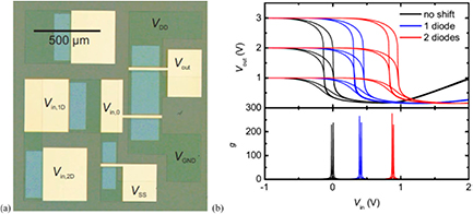
Figure 4. (a) Optical image of bipolar inverter based on ZnO/ZCO JFETs and diodes. The ZnO channels are seen as brighter blue green rectangles. The ZnCo2O4/Au gates and diodes are the yellow areas. (b) Inverter characteristics and gain values including the effect of the input voltage shift at the diodes for three values of the supply voltage VDD = 1, 2, and 3 V. © 2015 IEEE, reprinted with permission from [69].
Download figure:
Standard image High-resolution imageConcluding remarks.
Bipolar oxide devices offer many advantages such as ease of fabrication, stability, low voltage operation and high performance over rival concepts. However, steps towards better understanding of the physical mechanisms of transport across the p–n interface, the exploration of advanced p- and n-type oxides featuring high mobility and made from readily available elemental constituents as well as the development of a related technological platform are necessary to harvest all the potential benefits.
4. Complex-oxide field-effect transistors
Hans Boschker
Max Planck Institute for Solid State Research, Stuttgart, Germany
Status.
This section of the roadmap focuses on complex-oxide field-effect transistors (FETs). Here, complex oxides are defined as those oxides where the conducting electron/hole systems comprise d or f electrons. For an overview of oxide transistors using materials with s and p electrons, such as ITO, ZnO and BaSnO3, I refer to [16]. The electron systems of the complex oxides are strongly correlated and show rich emergent collective electronic behaviour. Therefore the main motivation to study complex-oxide transistors is to reveal how electronic correlations affect field-effect transistor operation and whether the correlated behaviour facilitates new types of logic devices [71].
Recently, FETs based on complex oxides that actually show current and voltage gain have been realized [72]. The key enabler is the electron system at the LaAlO3–SrTiO3 interface, discovered in 2004 by Ohtomo and Hwang [73]. This 2D electron system has a carrier density of 2 × 1014 cm−2 at room temperature and it is therefore possible to completely deplete the electron system with gate voltage smaller than a few V [72]. The electron system has a relatively low electron mobility of 10 cm2 V−1 s−1 at room temperature, mainly limited by strong electron-phonon scattering.
The state of the art LaAlO3–SrTiO3 transistors have a composite gate dielectric comprising a five unit-cell-thick LaAlO3 layer and a nine unit-cell-thick BaTiO3 layer (one unit cell is 0.4 nm) [74]. The dielectric constant of LaAlO3 is 24 and that of BaTiO3 is 300. This gate stack has a very high specific capacitance and is thick enough to prevent large gate leakage currents. The gate metal is gold and the source and drain contacts to the electron system are made from titanium. Figure 5(a) shows the transfer characteristic of a LaAlO3–SrTiO3 transistor. The transistors have been integrated into a ring oscillator circuit, whose output is shown in figure 5(b). Next to the previously discussed top-down lithographically patterned devices, also nanoscale devices have been written with AFM lithography [75].

Figure 5. (a) Transfer curves of a LaAlO3–SrTiO3 FET. The on/off ratio is six orders of magnitude and the subthreshold voltage swing is close to 60 mV dec−1. (b) A monolithically integrated LaAlO3–SrTiO3 ring oscillator. Upon increasing the supply voltage the output voltage oscillates with a RC time-constant-controlled oscillation frequency of 1.4 kHz. All data was measured at room temperature. Reprinted with permission from [74]. Copyright 2013 Wiley.
Download figure:
Standard image High-resolution imageOther materials that have been investigated for use as phase-transition transistors are VO2 [76–78] and SmNiO3 [79]. Recent field-effect studies using electrolyte gating of VO2 thin films demonstrate a huge switching effect where the channel conductance increases much more rapidly than the gate-induced charge-carrier density [77]. By inducing a metallic state in the surface layer with the gate, metallicity is induced in the entire thin film. This provides a large gain in the operation of transistors. However, it is not yet clear whether this switching behaviour is purely electronic; the field-induced creation of oxygen vacancies has been argued to be intimately related to the large increase of the conductivity [78]. Furthermore, transfer characteristics have not yet been measured, so it is unclear how these transistors compare to semiconductor devices.
Current and future challenges.
The crucial and as yet unanswered question is whether electronic correlations will facilitate electronics that can outperform standard FETs. With silicon technology reaching its fundamental performance limits, it is uncertain how electronics will advance beyond this stage. Graphene nanoribbon and carbon nanotube transistors receive much attention as a beyond-Si technology, because these materials have a much higher saturation velocity and thereby offer the prospect of faster devices. The physical basis of these devices, however, is unchanged with respect to silicon FETs. Correlated electron systems could facilitate logic devices based on fundamentally different switching mechanisms. In traditional field-effect devices, the applied voltages result in band bending but the band structure itself remains unchanged. In correlated electron systems, applied voltages can change the band structure, possibly leading to different physical limitations for transistor performance. For example, can an electron system that is driven through an intrinsic metal–insulator transition switch faster than 60 mV dec−1, the limit imposed by filling a rigid band structure with a thermal distribution of charge carriers?
The ideal switching device would be a high-density electron system that is switched with a small electric field between an insulating state with a sufficiently large bandgap, stabilized by either direct Coulomb interactions (Mott physics) or by electron-lattice interactions, and a metallic state, ideally with ballistic transport. Therefore one of the challenges is to obtain a material system where the intrinsic metal–insulator transition occurs far above room temperature, but that is still switchable. Interesting candidates are NbO2 and 2D Mott insulators such as LaTiO3–LaAlO3 and SrTiO3–SrVO3 heterostructures [80, 81]. Another challenge is to improve the high-field mobility of the complex-oxide materials. Currently mobilities are still too low for ballistic transport, but with a small improvement in materials quality and a drastic reduction of the device dimensions, high-enough mobilities are expected to be possible. Nanoscale devices are not only required to improve the device properties but also to study the underlying physics of the devices. Domain physics plays an important role in the physics of metal–insulator transitions [82]. To find out how fast these devices can switch, devices that incorporate only a single electronic domain are required. Thus, nanoscale patterning and processing of the complex-oxides materials is also a key challenge.
So far, LaAlO3–SrTiO3 transistors show characteristics similar to that of canonical semiconductor devices [74, 83], indicating that the effects of electronic correlations are small. The electron system at the LaAlO3–SrTiO3 interface has intermediate correlation strength, with effects due to electronic correlation predominantly observed at low temperatures. Therefore one of the immediate challenges is to build FETs from more strongly correlated materials. Furthermore, the strong spin-orbit coupling in f electron compounds has recently attracted large attention. It will be intriguing to see how the spin–orbit coupling changes the FET behaviour.
Advances in science and technology to meet challenges.
Complex-oxide epitaxy has made tremendous advances in recent years. This progress is due not only to improvements in the growth systems and growth monitoring, but also to a better understanding of the ways materials influence each other during heteroepitaxy. Materials properties are modified due to the presence of such phenomena as strain, polar discontinuities, and octahedral connectivity mismatch. This sensitivity offers the unique opportunity to optimize the complex oxides for use in devices. Recent achievements in this area are compositional interface engineering [84], modulation doping [85], oxygen octahedra rotation engineering [86], defect mitigation [74, 87] and improved stoichiometry control [88].
Another crucial development in technology that has been achieved recently is the feature-size reduction of both the correlated-oxide channel materials and the integrated metal structures such as the gates and source and drain contacts [83, 89]. Figure 6 presents a false-colour scanning electron microscopy image of a sub-100 nm LaAlO3–SrTiO3 transistor. The gate length is 60 nm, the channel width is 900 nm and the source and drain contacts are 30 nm separated from the gate. For the characterization of such devices and a discussion about short-channel effects, I refer to [83].

Figure 6. False-colour scanning electron microscopy image of a sub-100 nm gate length LaAlO3–SrTiO3 transistor.
Download figure:
Standard image High-resolution imageIntegration with very high-K dielectrics, such as BaTiO3, does generally not pose a large problem for the complex-oxide FETs. However, the more strongly correlated oxides require a larger charge-carrier-density modulation than that which can be achieved with high-K dielectric gate insulators. Here a solution may be found by using liquid electrolytes for gating. Electric-double-layer transistors achieve one order of magnitude larger charge-carrier-density modulation [77, 78]. But it remains to be seen how much electrostatic gating contributes to the induced charge-carrier density as opposed to electrochemical modification of the materials.
Concluding remarks.
The fabrication and study of complex-oxide field-effect transistors has made tremendous advances, and I expect this progress to continue in years to come. This provides a road towards answering fundamental questions about the physics underlying the performance of FETs using strongly correlated electron systems. Applications will certainly arise if the correlation effects facilitate better FET performance. In the meantime also niche market applications might emerge, especially because of the compatibility of the complex-oxide FETs with the wide spectrum of possibilities for electronics that is offered by the large variety of oxide materials systems.
Acknowledgements.
The author thanks J Falson, J Mannhart, C Woltmann, and members of the TO-BE Network, especially N Pryds, J Fontcuberta, and F Miletto Granozio, for valuable discussions.
5. Oxide electronic materials for resistive switching and TFT applications
Joynarayan Mukherjee1, M Priyadarshini1,2, Nandita DasGupta2 and M S Ramachandra Rao1
1 Department of Physics, Nano Functional Materials Technology Centre and Materials Science Research Centre, Indian Institute of Technology, Madras, Chennai 600036, India
2 Microelectronics and MEMS laboratory, Department of Electrical Engineering, Indian Institute of Technology, Madras, Chennai 600036, India
Status.
Oxide electronic materials offer plenty of opportunities to probe into many fundamental physical properties and provide ample application prospects in opto-electronics, information storage devices, displays, LEDs, fuel cells, batteries and many more. Figure 7(a) shows the assorted functionalities offered by oxide electronic materials. Many metal oxides show resistive switching (RS) behavior, wherein by varying the applied voltage, the resistance of the metal oxide switches from high resistance state (HRS) to a low resistance state (LRS) and vice-versa. Also, metal oxides due to their wide bandgap and high mobility even in amorphous state find applications in thin film transistors (TFTs) which are primarily used as switching devices in displays. Out of the many exciting phenomena oxide materials exhibit, in this article we will focus on the mechanism and the device aspects of resistive switching and TFTs for display applications.
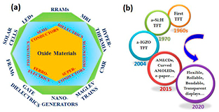
Figure 7. Schematic showing (a) different physical properties and applications of oxide materials. (b) Evolution of thin film transistor technology and its potential future applications.
Download figure:
Standard image High-resolution imageResistive switching.
The resistive random access memory (RRAM) has gained considerable attention both in academia and industry for its application in non-volatile memory (NVM) devices. RRAM has the advantages of high density, high operation speed, multibit storage, low power consumption and simple device structure [90]. A wide variety of binary and multi-component oxides show resistive switching behavior. Based on the polarity of the applied bias, RRAM can be categorized in two types: (i) unipolar resistive switching and (ii) bipolar resistive switching. Unipolar resistive switching is usually observed in binary oxides such as NiO, CuOx, TiO2, ZrO2 and Nb2O5 whereas bipolar resistive switching has been reported on both binary and ternary oxides like Al2O3, Pr0.7Ca0.3MnO3, and InGaZnO4.
Thin film transistors.
TFTs are the backbone of display technology and are used in different devices like TVs, smartphones, tablets, laptops, e-readers, and wearable displays etc. TFTs using oxide semiconductors were commercialized in flat panel displays for the first time in 2012 and since then they have been used in a plethora of applications. A schematic of how oxide technology has evolved over the years and the tremendous applications offered for the future is shown in figure 7(b). Different metal oxides with constituent cations of Zn, Sn, Ga and In can be used for the channel layer of the TFT. Among different metal oxides, InGaZnO4 has been the most successful oxide material for use in displays due to its several advantages like high mobility in amorphous state, low leakage current, low temperature processing and TFTs based on IGZO have commercial advantages like lower power consumption, higher sensitivity, reduction in pixel size and higher resolution [91]. However indium is a rare element with low abundance in Earth's crust. It is also costly and toxic, which limits its long term use.
Current and future challenges.
Resistive switching.
Although RRAM has many advantages there are some issues, such as the large variation in the set and reset voltages, which need to be overcome. It is very important to understand the microscopic origin of the resistive switching behavior for better device performance. The mechanisms such as formation and rupturing of filament and migration of oxygen vacancies in the switching layer play a crucial role in the RS phenomena. Recently, in situ TEM study showed the formation and rupture of conducting filaments during RS operation in ZnO thin films [92]. Though there are many models reported in the literature, more experimental evidence is required to understand the mechanism behind the switching phenomena. Moreover, another important issue regarding the commercialization of RRAM is the large variation in set and reset voltages which leads to switching failures.
Thin film transistors.
For use in TFTs, binary oxides like ZnO, SnO2 can primarily be used. However, it is very difficult to deposit these films with amorphous microstructure and they tend to have high density of carriers even in as-deposited state which makes it difficult to modulate the channel conductivity [93]. ZTO on the other hand has amorphous structure and is a promising indium and gallium free material for consideration. One of the problems limiting fabrication of ZTO based TFTs is the difficulty in etching ZTO. ZTO is chemically stable and resists most of the etchants and it becomes more difficult to etch it with increase in tin concentration [94]. Also, ZTO involves higher processing temperature compared to IGZO. Another material considered is TGZO, but it is found to have poorer performance when compared to ZTO. It is more costly due to the presence of gallium in the system and has etching problems [95].
Advances in science and technology to meet challenges.
Resistive switching.
In the early 1960s, resistive switching phenomena in thin oxide layers of Al, Nb, Si and Ti was reported [96]. In 1994, Bloom et al showed the resistive switching behavior in ferroelctric PbTiO3 [97]. Since then, many materials have been investigated as RRAM candidates. Companies such as Samsung Electronics and Hewlett-Packard have been making serious attempts for the commercialization of RRAM based memory devices. Today, the vital challenge for the RRAM is the storage density which can be overcome through the stacking structure [98]. The other way to increase the storage density is the using of multibit switching property. Multistate resistance can be realized in a unipolar device by tuning the filamentary path [99] and for the bipolar device by varying the defect concentration [100].
Thin film transistors.
Several attempts have been made to etch ZTO using wet chemical methods, unfortunately without a very promising solution. To date the reported wet etching processes show a very narrow process window making it difficult to use them consistently [101]. Costly techniques involving plasma techniques and dry etching using chlorine currently seems to be the only plausible way. Techniques such as solution combustion synthesis [102], deep-ultraviolet (DUV) photochemical activation have recently been explored for reducing the processing temperature. DUV photochemical activation has shown promising results even for room temperature deposition with comparable performance and operational stability as that of high temperature (⩾350 °C) annealed devices [103].
Concluding remarks.
There is plenty of room for using oxide materials in different applications such as logic/rf circuits, memories, radio-frequency identification tags, transparent electronics, medical patches, image sensors and printed electronics. Among other NVMs, RRAM is more promising for next generation memory devices. The microscopic mechanisms need to be investigated to improve the device performance in terms of its size and speed. Oxide materials will continue to play a key role in next generation displays which require that the materials be used are sustainable and cost effective. ZTO is one such material which holds potential to revolutionize the display industry. Advancements in newer etching techniques and methods to process it at lower temperatures are essential to realize the full benefit of this material.
6. Application aspects of ZnO
David J Rogers, Ferechteh H Teherani, Eric V Sandana and Philippe Bove
Nanovation, 8 Route de Chevreuse, 78117 Châteaufort, France
Status.
A recent study by Nanomarkets estimated a market value of over 500 million € for electronics based on ZnO. This commercial success is based on ZnO's versatile property set combined with low materials cost and an ongoing series of technological developments [104].
The most mature ZnO electronics applications are anti-static layers, electromagnetic interference shielding and optical coatings. Indeed, ZnO is semiconductor with a widely tuneable conductivity and it can be deposited in large-area thin film form at high rates and low temperatures using a number of techniques including sputtering, pulsed laser deposition, chemical vapour deposition and solution based processing. On the optical front, ZnO brings excellent transparency right across the visible spectrum while the plasma frequency can be engineered to reflect environmental IR radiation (e.g. in energy efficient windows) and the bandgap (Eg ~ 3.4 eV) blocks UV light (e.g. in welding glasses). UV filtering has been extended to transparent sun creams using ZnO nanoparticles under ~60 nm in diameter that do not scatter visible light. Such nanoparticle manufacturing testifies to the biocompatibility of ZnO as a basis for the development of nano ZnO based electronics [105].
The largest current electronics application of ZnO is that of varistors for voltage surge protection. Varistors are based on the formation of double Schottky junctions at ZnO grain boundaries in sintered ZnO powders (~10 µm grains) which act as a collection of back-to-back Zener diodes. Due to the high melting point of ZnO (~1975 °C) such varistors can support the heating associated with large current flow. ZnO displaced SiC as the dominant varistor material when it was discovered that doping with metal oxides (of Bi, Pr, Co, Mn ...) gives the most non-linear I/V characteristics known so far [106].
Another long standing use of sintered ZnO powders is for the fabrication of gas sensors. These function based on the principle that absorption or desorption of a gas at the surface and grain boundaries changes the conductivity. ZnO was adopted because it was inexpensive and gave a competitive sensitivity combined with high mechanical/chemical stability and low toxicity. Furthermore, a new generation of compact, low-power nanostructured ZnO gas sensors is currently emerging [110]. Thanks to a very large surface-to-volume ratio such devices have shown the capability of sub-parts-per-million (ppm) sensitivity for a number of molecules, including C2H5OH, CO, H2, H2O, H2S, NH3, NH4, NO2 and O3.
Wurtzite ZnO also offers a polar crystal structure with amongst the highest piezo-reponses of any semiconductor. Furthermore, sputtered ZnO films show better quality and adherence to a-SiO2/Si than alternative materials with larger piezo-responses. This capacity for monolithic integration with silicon-based electronic circuitry, along with an amenability to chemical processing has led to ZnO being adopted for use in surface acoustic wave multiplexing/demultiplexing bandpass filters for telecommunications applications, primarily cellular phones and base stations. In these devices the challenges of processing, contacting and packaging ZnO thin films on an industrial scale has been mastered [107].
ZnO has also been very widely used as a green phosphor in vacuum fluorescent displays based on the efficient oxygen vacancy emission in zinc rich ZnO. Recently, this market has waned, however, due to the advent of novel display technologies.
Current and future challenges.
Up until the present, the most widely used transparent conducting oxide has been Sn-doped In2O3 (ITO). Doped ZnO is currently a challenging ITO, however, for applications such as transparent wiring, touch-sensitive panels and transparent electrical contacts (for use in flat panel displays, solar cells—particularly a-Si and CIGS—and LEDs) [108]. This is because it is cheaper, abundant, less toxic, easier to process, shows superior resistance to hydrogen plasmas and can be fabricated at lower temperatures. Moreover, the mobilities and conductivities attainable with degenerately doped ZnO (typically with Al, Ga or Si) have become comparable with ITO. The main challenge remains the displacement of the installed base for production of ITO.
Recently, transparent field effect transistors employing amorphous ZnO-alloy channels (typically indium–gallium–zinc–oxide) and electrodes have emerged [108]. These are enhancement mode devices (no power consumption in off state) which have low leakage currents, exhibit impressively high on/off ratios (>108) and have channel mobilities that are more than an order of magnitude higher than current a-Si:H based TFTs. Thus they are being adopted for use as select transistors in active matrix LCD screens, electronic paper and flexible OLED panels. Higher mobility offers increased refresh rates, improved transparencies allow smaller pixels (with reduced aperture ratios) and the wide bandgap reduces light sensitivity (lower noise) and degradation. The materials also have the potential for low temperature, low-cost, wide area, high throughput solution based fabrication. The main challenge is displacement of the installed base for industrial production of a-Si:H based devices. For more on this topic see the sections by section 2 and section 5 in this roadmap.
The use of ZnO as a UV photodetector has received much attention of late, because the bandgap can be tuned from the UVA into the UVC by alloying with Mg while maintaining the wurtzite phase, figure 8 illustrates the alloying potential for bandgap engineering of ZnO in contrast with that for GaN [109].
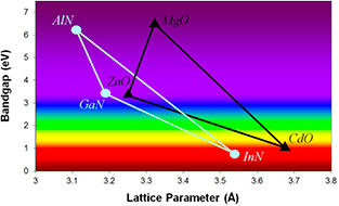
Figure 8. The relationship between Eg and lattice constant is shown for alloys of wurzite (Al,ln)GaN and (Mg,Cd)ZnO. Although UV bandgap engineering of ZnO is typically achieved by such alloying with Mg, deeper UV performance (up to 10.6 eV) can be achieved by alloying with BeO. There are toxicity and handling issues in this case, however.
Download figure:
Standard image High-resolution imageCurrent state-of-the art (Mg)ZnO PD are usually based on metal–semiconductor–metal (MSM) architectures. An MSM-PD is made by forming two inter-digited transducer Schottky electrodes on n-type (Mg)ZnO. Such PD exhibit sharp visible wavelength cut-off, low dark currents, high speed operation, linear signal response with optical power and extremely low parasitic capacitance/noise. These characteristics make them attractive for sensing and imaging applications (e.g. aerospace, automotive, military, petroleum, flame detection and astronomy). The main challenges are to compete with alternative solid state UV PD based on SiC (already available) and (Al)GaN (emerging). However, the insertion of high pass filters is necessary with SiC (bandgap engineering is not possible) and (Al)GaN detectors are difficult/expensive to fabricate.
ZnO is also emerging for biosensing (piezoelectric, electrochemical, optical or field effect transistor based transduction) [111]. Good electrical conductivity, chemical stability, a biomimetic nature, the potential for surface functionalisation and a high isoelectric point (which facilitates immobilization of biomolecules) make ZnO an attractive biosensor matrix. Due to their small dimensions, increased sensing surface and strong binding properties nanostructures offer faster responses and can achieve single-molecule detection. Ongoing trials should pave the way to commercialisation of implantable, miniature point-of-care biosensors compatible with CMOS/MEMS technology for wireless telemedicine.
With almost 8000 publications on ZnO in 2015 (see figure 9) it is impossible to examine all the potential future applications in this section. Some promising emerging topics are memristors, waveguides, extreme (high temperature/field/radiation/frequency) electronics, nanoelectronics, electron scintillators, piezotronics, piezogenerators, thermoelectrics, dye sensitized solar cells, photoelectrochemical hydrogen generation, actuators, plasmonics, phononics, spintronics and solar cell light/current management. Also of note is that a recent Thomson-Reuters study, recorded more publications dedicated to nanostructured ZnO than to carbon nanotubes. This was attributed to the multifunctional nature of ZnO, the ease of fabricating nanostructures by various techniques (including wide-area, low cost chemical growth) and the extremely large family of nanostructure shapes that can be obtained.
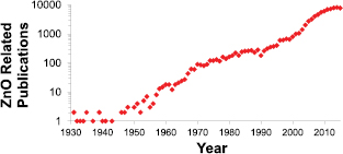
Figure 9. The number of annual publications versus year, according to a search of the Scopus database for the term 'zinc oxide' in the abstract, title, or keywords.
Download figure:
Standard image High-resolution imageAdvances in science and technology to meet challenges.
A fundamental outstanding challenge for ZnO-based electronics is the achievement of efficient p–n junction devices. Indeed, ZnO is considered as a potentially superior UV emitter to GaN (currently the commercially predominant opto-semiconductor) because of the higher stability of the ZnO free exciton, which has a binding energy of 60 meV (compared to 21 meV for GaN) (see section by J Zuniga-Perez in this roadmap). It has proven difficult, however, to incorporate and activate sufficient acceptor concentrations. Moreover, background donors tend to compensate the acceptors because native defects (O vacancies and Zn interstitials) in combination with common background impurities (such as H, Al and Ga) act as shallow donors in ZnO. Recently, many groups have reported significant progress in the development of p-type ZnO [112] allowing the demonstration of light-emitting p–n junctions [113]. The main acceptor dopants adopted are the Group V elements N, P, As, Sb plus the Group Ia elements Li, Na, K and the Group Ib elements Ag, Cu, Au. There are various competing theories as to how the dopants act but experimental results generally show mobilities, conductivities and overall device efficiencies that are relatively disappointing. The recent development of high quality native substrates and the adoption of higher purity sources have helped to suppress defect densities and non-intentional impurity doping respectively and thus reduce donor compensation. Another emerging factor is that Mg alloying could facilitate the task of p-type doping. The two main reasons put forward for this are the shifting of the conduction band to higher energy acting to reduce the background donor concentration and the Zn vacancy (acceptor) concentration increasing with Mg content. For more on oxide p–n junction devices see the section by M Grundmann in this roadmap.
Concluding remarks
The broad range of existing and emerging applications described above testifies to the combination of multifunctionality, commercial relevance and manufacturability offered by ZnO. If the efforts towards p-type ZnO continue to advance, we can expect to see this extend to bipolar and complementary (n- and p-type) devices as the basis for brighter and more robust excitonic-based UV emitters (with lower lasing thresholds), ultra-sensitive UV photodetectors and fully-integrated transparent electronics.
7. All-oxide photovoltaics
Kevin J Rietwyk and Arie Zaban
Department of Chemistry, Center for Nanotechnology & Advanced Materials, Bar Ilan University, Ramat Gan 52900, Israel
Status.
All-oxide photovoltaics is a promising family of low cost thin film solar cells. With so many metals being abundant and the ability to grow stable, thin film oxides in low vacuum and ambient environments, metal-oxide based solar cells enjoy low fabrications and raw material costs. In addition, metal-oxides typically possess the high chemical stability and low toxicity desired for photovoltaic devices. Due to the various functional properties of metal-oxide compounds, a range of architectures are possible for all-oxide photovoltaics based on conventional photovoltaic, bulk photovoltaic, ferroelectric domain walls, plasmon-enhanced hot-electron injection, nanocomposite materials and even thermoelectricity. The energy diagrams for some of these cells are given in figure 10.

Figure 10. Schematic band diagrams of all-oxide photovoltaic cells. (a) Conventional ZnO|Cu2O heterojunction. (b) Single layer Bi2FeCrO6 bulk-photovoltaic cell before (left) and after (right) poling with 10 V showing polarisation induced change in the energetics. (c) Lateral BiFeO3 cell showing four ferroelectric domains and domain walls (actual cells are typically comprised of hundreds). d) TiO2|Ag plasmon-enhanced hot-electron injection cell in which hot electrons from optically excited plasmons in the Ag are transported through TiO2 to an FTO layer, before cooling.
Download figure:
Standard image High-resolution imageThe conventional photovoltaic effect is by far most common, in which, a gradient in the electrochemical potential in the absorbing semiconducting layer is used to separate optically excited electron-hole pair which are collected at different electrodes. The performance of these devices is enhanced by utilising selective contacts to promote limit the transport of carrier species to select electrodes. The highest efficiency achieved for this group of all-oxide solar cells is 5.38% and are based on a Cu2O|ZnO (pn) heterojunction with a Ga2O3 buffer layer [114].
For solar cells based on the bulk photovoltaic effect, a photovoltage is generated in non-centrosymmetric (ferroelectric) crystals due to a polarization induced electric field (depolarisation electric field) which promotes the charge. In a recent Nature Photonics paper by Nechache et al [115] an efficiency of 3.3% for single absorber layer and 8.1% for multi-layered solar cell was attained, greatly surpassing the previous record for single layered cells of only 1.25% whilst demonstrating the feasibility of this design.
In an alternate, lateral design that also exploits ferroelectricity, a series of thin layers of a ferroelectric material are grown with regularly spaced conductive, ferroelectric domain walls. Each domain acts like a small cell and the walls produce an electric field in the adjacent domains that separate the charge carriers. While each domain produces a photovoltage only in the order of 10 mV, the domains are linked in series and with hundreds of domains large voltages in excess of 15 V can be produced [116].
Plasmon-enhanced hot-electron injection based solar cells are rapidly gaining popularity. The operation depends on optically excited carrier plasmons which decay into hot electron-hole pairs. These carriers then separate at the metal/semiconductor interface and are collected before cooling. The energy of the plasmon is tuned using nanostructures to within the visible light region to ensure optimal current. Barad et al [117] recently developed a method to grow very low cost plasmonic solar cells via the deposition of thin films of silver onto a sprayed pyrolysis deposited TiO2 layers in which the high surface roughness of the TiO2 is exploited to form the silver nanostructures.
An interesting hybrid technology is solar thermoelectric generators (STEG) in which concentrated solar radiation is used as the heat source for a thermoelectric generator. Since the efficiency is dependent upon the temperature difference across the generator, oxides are an excellent candidate group—commonly exhibiting high-temperature (~1000 K) stability in air while enjoying reasonable thermoelectric properties. Terasaki et al [118] have reported 1.4% efficiency for preliminary BiSrCoO/CaYbMnO uni-couple devices.
Current and future challenges.
In order for all-oxide photovoltaics to break through into commercial markets, it is necessary to raise the efficiency of the devices. Metal-oxides are an essential building block in modern thin film technology and have proven effective in their role in many photovoltaics and electronic devices as transparent conductors (FTO, ITO, AZO), carrier selective contacts (TiO2, ZnO, V2O5, NiO, WO3, MoO3), and ultra-thin buffers layers (Al2O3, Ga2O3) [119]. The chief shortcoming in all-oxide photovoltaics is a lack of metal-oxides with a suitable suite of properties to perform as ideal light absorbing layers [120].
To achieve high performing solar cells it is important for the absorber layer to possess a range of optical and electronic properties with the most quintessential property being the band gap. Only photons with energy greater than the band gap can be absorbed and contribute to the photocurrent. For traditional devices, there is an additional balancing with the energy of photons that provide the photovoltage, limiting the ideal band gap to 1.34 eV for a single junction solar cell [121]. For other designs, it is essential that the absorbing material possess other key properties such ferroelectrical behaviour or carrier plasmons with appropriate energies.
Once optically excited, for carriers to be collected, the absorber layer must also possess excellent transport properties including high carrier mobilities and a low concentration of trap states and recombination centres. In addition to the internal electric field, these qualities determine the distance carriers can propagate before recombining and as a rule-of-thumb the minority carrier diffusion length should be greater than the optical absorption depth.
Finally, the collection of the carriers from the absorber layer is determined by the interfaces with adjacent layers. For optimal performance, there should be minimal defects at the interfaces and appropriate energy level alignment to ensure transfer of a single carrier species at each interface.
Advances in science and technology to meet challenges.
While the physical properties of most binary metal-oxides have been extensively investigated, only a fraction of all the possible ternary and even fewer quaternary metal-oxides have been studied. The number of possible chemical compositions and structural phases increases exponentially with the quantity of elements involved, and the combination of both define their set of physical properties. Therefore, it stands to reason that countless metal-oxide compounds with the ideal set of properties for photovoltaic applications exist and have yet to be found. Unfortunately, for complex compounds it is exceedingly difficult to predict the properties of oxides using empirical methods, so it is necessary to perform a large scale search for suitable materials and this requires a high-throughput methodology [122].
The search for new materials can be undertaken using computational materials engineering and/or experimental combinatorial material science. Both methods involve high throughput examination of unknown materials and utilise tools to generate knowledge from the acquired information, which is stored in readily accessible databases along with relevant metadata to enable rapid analysis. The combinatorial material cycle is summarised in figure 11. For the rest of this section we will focus on the experimental efforts, for reasons of brevity.

Figure 11. Combinatorial development cycle for all-oxide PV.
Download figure:
Standard image High-resolution imageCompared to their computational counter-parts, there are fewer high-throughput experimental efforts due to the large overhead required to establish the experimental instrumentation. To perform studies, metal-oxide compounds are grown on large substrates (on the order of 50 cm2) using co-depositions of different oxides to produce films with spatially varied chemical composition. The resulting layer is characterised using a series of automated scanning robots that perform local area measurements sequentially in an array of positions across the sample. The selection of suitable analytical techniques is diverse and includes any non-destructive, scanning measurement. The results of each technique can then be related to each other to identify relationships between composition and the various physical properties. The experimental approach enjoys the capability of only producing realistic material structures and can be employed on a wide range of specimens from single material layers up to complete devices.
Experimental efforts would benefit greatly from the development and implementation of big data and machine learning tools. Machine learning algorithms can rapidly enhance data treatment rates by providing automated background subtraction and deconvolution of spectral data to identify onsets and peak locations, width, areas and so on [123]. This information can be used as metrics for clustering algorithms or datamining activities that enable high dimensional data analysis to identify complex trends, such as quantitative-structure-activity relationship and process-structure-physical property relationship analyses [124].
Concluding remarks.
Although efficiencies are currently low, the ability to develop all-oxide photovoltaics from low-cost raw materials and fabrication methods makes them a realistic option for cheap solar cells. Improvement in device performance, comparable to contemporary commercial solar cells, is expected to be achieved via high-throughput investigations into new metal-oxide compounds. However, given the wide range of possible architectures and designs available to this versatile family of materials, the exact form that future all-oxide photovoltaics will adopt is both unpredictable and very exciting.
8. Perovskite-type materials for energy converters
Angelika Veziridis and Anke Weidenkaff
Materials Chemistry, Institute for Materials Science, University of Stuttgart, DE-70569 Stuttgart, Germany
E-mail: weidenkaff@imw.uni-stuttgart.de
Status.
Perovskites are a unique class of compounds due to their wide-ranging electronic, chemical and mechanical properties. Their composition can be varied on a large scale (subject to the Goldschmidt tolerance factor) without substantial change of the crystal structure. This flexibility allows the incorporation of a vast range of elements modifying the attractive physical and chemical properties. Thus, substitution materials free of critical elements can be created, which is a prerequisite for device application. They have a particularly huge potential for many energy conversion processes due to their insulating, p- or n-type semiconducting, metallic or even superconducting transport properties. Ferroelectric, piezoelectric, catalytic or thermoelectric materials are also known in this family [125].
Major challenges such as global warming and the finite nature of fossil fuels can only be met by the development of renewable resources and new energy conversion and storage technologies. For this purpose, nothing short of temperature- and oxidation-resistant, non-toxic compounds based on abundant, noncritical and inexpensive elements are required. Perovskite-type transition metal oxides (figure 12) do meet these conditions and are already widely used for energy conversion processes. Applications include but are not limited to thermoelectrics, photovoltaics, photoelectrocatalysis and fuel cells.
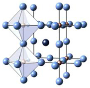
Figure 12. Ideal cubic perovskite crystal structure: the B cation (brown) is octahedrally coordinated with six X anions (lilac) forming an infinite array of corner-sharing BX6 octahedra, The A atom (dark blue) is located in the center of eight octahedra.
Download figure:
Standard image High-resolution imageCurrent and future challenges.
Thermoelectricity (TE) is the direct conversion of thermal energy into electricity and vice versa. Therefore, TE is a versatile technology to improve many technical and industrial processes, which for thermodynamic reasons discharge heat (e.g. fuel cells (figure 13(a)) [126]). The challenges regarding the widespread implementation of this technology lie in the high cost and low efficiency of TE systems. The TE conversion efficiency increases with increasing temperature gradients across the material due to higher Carnot efficiencies. But the currently best-performing TE materials (Bi- and Pb-containing chalcogenides) lack stability at higher temperatures due to decomposition, vaporization and melting.

Figure 13. (a) Hexis SOFC cell stack and (b) thermoelectric oxide modules (TOM) made of perovskite-type oxides.
Download figure:
Standard image High-resolution imageThe interest in perovskite-type oxides derives from their temperature stability, their correlated electronic structures enabling additional band structure tuning, the cost-effective and non-toxic constituents. Particularly manganese and titanium oxides are considered promising n-type materials while cobalt oxides have been identified as suitable p-type materials with a reasonably high TE performance to build all oxide thermoelectric converters (figure 13(b)). This is due to both a suitable crystal and electronic structure enabling adjustment of TE-relevant transport properties.
Using the example of SrTiO3, the possibility of Ti4+ → Ti3+ transition metal reduction provides the basis for increasing the charge carrier concentration and mobility by appropriate A- and B-site substitution and deficiency, respectively. In addition, a well-defined defect chemistry induced by the synthesis conditions also ensures effective phonon scattering reducing the counterproductive thermal conductivity. In a comparative study of different A-site-substituted SrTiO3 compounds a maximum high-temperature ZT value of 0.42 was measured [127].
Moreover, nano-structuring using well-established and scalable soft-chemistry synthesis techniques combined with stepwise sintering further improves the TE-properties of perovskite-type oxides. This was revealed by B-site substituted CaMnO3-δ compounds resulting in peak ZT values >0.2 at 1160 K [128].
Photovoltaics (PV) is probably one of the most widespread sustainable energy conversion technologies. The efficiency depends on the ability of the PV material to absorb solar light, to separate electron and hole pairs, and to transport the carriers, which makes demands on the band gap, a built-in electric field and the carrier diffusion length.
In recent years, the class of intrinsic semiconductors has become an alternative to conventional PV materials. Their most important advantages is that the thickness of the active materials can be reduced lowering the internal resistance of the cells. In a minimum of time, solar cells based on hybride halide perovskites have made very rapid progress.
Meanwhile, the search for suitable, more stable inorganic perovskite oxides continued, mainly because of their comparatively higher robustness to moisture. The multiferroic BiFeO3 (BFO) is the most intensely studied compound for this purpose due to its solar light-suited band gap and the internal electric field. But in contrast to their hybrid counterparts, the conversion efficiency of BFO-based both single-layer devices and heterojunctions currently remains below 10% [129]. The multifunctional behavior of BFO is due to a slight strain in the structure. In order to improve and model the material, a better understanding of how external and internal stimuli affect the properties such as carrier concentration and recombination is required in the first place.
The economic advantage of perovskite oxide-based PV modules might be their simpler processing and absence of environmentally hazardous heavy metals. Instead of challenging well-established products, a cooperative approach in terms of tandem cells appears more promising [130].
Direct conversion of solar into chemical energy is accomplished by means of photoelectrocatalysis. This is particularly interesting for the production of hydrogen as storage medium in a sustainable energy management system. But up to now there are no materials or device setups offering sufficient efficiency and stability for direct solar water splitting.
Perovskites based on the abundant element titanium can be an alternative. They are a natural choice to replace pristine or doped TiO2 allowing for band gap tuning by anionic along with simultaneous cationic composition modification. Partial anionic substitution of oxygen for nitrogen leads to the formation of oxynitride perovskites, a group of compounds with interesting physicochemical properties attributed to the resulting changes in the electronic band- and defect structures [131]. Synergetic effects with ferroelectric or piezoelectric properties might be an asset.
The water splitting process involves separation of charges and their fast transport to the device surface. Therefore, the absence of anionic vacancies is crucial because they act as recombination centers. Two basic concepts are used to avoid an additional formation of vacancies inside the perovskite crystal structure due to charge neutrality: Partial substitution of trivalent (e.g. La3+) and five/six-valent (e.g. Ta5+, Mo6+) cations for the A- and B-site cations, respectively, or partial substitution of equal amounts of nitrogen and fluorine for oxygen [132].
Another challenging task is the further processing of synthesized phases to a photoelectrochemical device with lasting high performance. Especially, the preparation of dense bulk samples to ensure a high mobility of generated charge carriers is suffering from limited thermal stability of the oxynitrides.
The advantages of solid oxide fuel cells (SOFC) converting chemical into electrical energy are their high efficiency and fuel flexibility. In recent years, considerable efforts have been made to lower the operating temperature for cost and stability reasons. This virtually requires the development of a whole new set of tailor-made materials with adequate reactive and regenerative properties in a broader temperature range.
Perovskite-type La/Sr/Mn oxides are already the most commonly used SOFC cathode material. Replacing Mn for Co/Fe improves the electric conductivity and catalytic efficiency at lower temperatures. But cation segregation at elevated temperatures under electrochemical polarization can considerably impair the cathodic performance. Additional long-term surface poisoning by impurities (e.g. Cr evaporating from steel interconnects) might lead to degradation [133].
Perovskites have also been explored as solid-state electrolytes with high oxygen conductivities and low exchange resistance. Unfortunately, the studied LaGaO3-based materials form secondary phases with the used cathode materials, as high oxygen mobility is inevitably associated with weaker bonds and hence lower stability. Accordingly, they are also sensitive to the reducing conditions at the anode leading to decomposition or unwanted electron conduction. These side effects might be controlled by using composites of perovskites and the conventional electrolyte yttrium-stabilized zirconia (YSZ). In addition, this approach also reduced grain boundary resistance and increased the ionic conductivity [134].
Several Mo-containing double-perovskite phases have been proposed as anode material in the low temperature range. The challenges are similar to those of the cathode materials: stability at reducing conditions, electrolyte compatibility and specific resistance.
Perovskites have also been suggested as interconnect materials needed for stack formation. LaCrO3-based compounds are particularly promising owing to their sintering properties, electronic conductivity and mechanical strength.
Advances in science and technology to meet challenges.
The characteristics of perovskite-type compounds depend on their electronic structure. For the design of material properties geared to a defined application, the '3 D strategy' has proven the treatment of choice: Density of states (electronic band structure), Defects (traps, in-gap states) and Dynamics (catalysis, regeneration).
The density of states (DOS) is a function of the crystal lattice, spin states, dimensionality of the crystallites (quantum confinement) and correlation effects. It determines the chemical potential (Fermi energy, EF) as well as the band gap and thus the transport properties of the material. Defects exist in every solid and govern the so-called 'Realstruktur' with the catalytic sites. They can dramatically modify the electronic properties as they add states to the band gap. This 'out-of-equilibrium' situation is the fundamental driving force for all energy conversion and catalytic processes. Eventually, the dynamics of catalytic and energy conversion processes play a vital role for the performance of materials.
Control of the material properties by means of the elemental composition presupposes the precise knowledge of the above-mentioned correlations. Additionally, also the synthesis method has a marked influence on the properties through, for instance, density, surface area and microstructure of the compound. Only the appropriate consideration of all these aspects allows development of improved and competitive oxide materials.
Concluding remarks.
Better energy conversion processes require materials with desired properties tailored to the respective application. The versatile perovskite structure ABX3 is a suitable basis for this purpose. Its remarkable stability provides the opportunity to use most elements of the periodic table as well as organic ions on the A-, B- and X-sites.
In view of a target-oriented approach, this plethora of possible combinations demands theoretical models to predict the material properties under operating conditions. In order to minimize the risk of degradation in harsh environments, appropriate measures such as coatings, (nano-)composites or modified microstructures have to be taken to ensure a reasonable service life. Therefore, a better knowledge of the mechanisms involved in surface and transport reactions (along with improved operando characterization and modelling techniques) is the essential precondition to design materials with better performance and stability for sustainable energy converters of the future.
The flexibility of perovskite-type oxides facilitates to comply apart from conversion efficiency with additional very important constraints such as abundance, toxicity and environmental benignity. In the end, they have to be cost competitive with conventional technologies.
9. Superconductivity in oxides: from processing to applications
Miryala Muralidhar and Masato Murakami
Superconductivity Research Laboratory, Graduate School of Science and Engineering, Shibaura Institute of Technology, 3-7-8 Toyosu, Koto-ku, Tokyo 135–8548, Japan
Status.
High temperature copper-oxide superconductors (HTS, cuprates) possess significant potential for various high-field applications due to their high superconducting transition temperature (Tc) and upper critical field (Bc2) values. However, the giant relaxation causes that the above limit of applicability of HTS materials is reduced from Bc2 to Birr, the irreversibility field. Due to rather strong anisotropy of cuprates, their irreversibility field is angularly dependent and reaches the lowest value just for magnetic field parallel to the c-axis, the configuration particularly important for many applications. The relaxation and thus also Birr value are controlled by the operating temperature and by effectiveness of pinning at this temperature. Anyway, cuprates can trap magnetic fields by an order of magnitude higher than the best classical hard magnets and are therefore promising as permanent magnets. In this roadmap, recent development in processing, production, flux pinning and applications of cuprates is presented and discussed.
In the polycrystalline form the high-Tc materials can carry only low critical current densities, due to grain boundaries (weak links) and crystal anisotropy. The numerous attempts to improve the critical current density have resulted in development of a variety of processing techniques among which the most successful one is the top seeded melt-texturing [135, 143]. In this process, the superconducting phase (REBa2Cu3Ox, RE = yttrium or a rare earth) is formed by a peritectic reaction of RE2BaCuO5 (2 1 1) with the liquid phase (BaCuO2 and CuO). The growth process of the superconducting phase starts from a suitable seed crystal and is accelerated by means of fine homogeneously dispersed 2 1 1 phase in the liquid phase; rests of the not reacted 2 1 1 phase serve as pinning precipitates dispersed in the superconducting phase. Especially the materials with light rare earths, LREBa2Cu3Oy (LRE: Nd, Sm, Gd, NEG etc), produced by means of the oxygen controlled melt growth technique show rather high irreversibility field (>5 T, H//c-axis) and critical current density (Jc) of the order of 106 A cm−2 at 77 K [136]. Moreover, due to tendency of LRE ions to exchange positions with Ba in the crystallographic lattice, a special point-like disorder is formed in the LRE-123 materials that contributes to formation of the peak effect at moderate magnetic fields [137]. The beauty of melt textured LRE-123 materials is that a superconducting pellet can be magnetized to a high external magnetic field, and then, a large part of the field is trapped in the pellet upon removing the external field. The field trapping capability of melt-textured materials depends on the critical current density and the single grain size [138] (figure 14, left). Thus, an improvement of the critical currents, in particular at high magnetic fields and at high temperatures above LN2 are crucial for the successful introduction of these new magnets to the market.
Figure 14. A photo graph of batch processed as grown single grain Gd-123 samples prepared by the top seeded met growth process (left); nanometer sized Gd-211 secondary phase dispersion in NEG-123 matrix (left middle); permanent Fe-Nd-B magnet stably levitating over an NEG-123 material at 90.2 K (right middle); a magnetized NEG-123 pellet suspended below another NEG-123 permanent magnet (right).
Download figure:
Standard image High-resolution imageCurrent and future challenges.
The electromagnetic performance of LREBa2Cu3Oy has reached the level required for industrial applications and bulk superconducting magnets will be able in a close future to enter the market as basic parts of various utilities. While at moderate magnetic fields nanoscopic point-like defects play an important role, at low magnetic fields rather large secondary phase particles are effective. A successful refinement of the secondary phase particles up to nanometer level (figure 14, middle left) results in a considerable increase of super-current density. The (Nd,Eu,Gd)Ba2Cu3Oy 'NEG-123' samples exhibit not only the highest Jc ever reported for bulk samples but also enable (for the first time) levitation at liquid oxygen temperature (90.2 K) (figure 14, right) [139]. Another milestone in the LRE-123 materials' performance was reached by doping the melt-textured (Nd0.33Eu0.33Gd0.33)Ba2Cu3Oy + 35 mol% Gd2BaCuO5 (70 nm in size) composite by tiny amounts of nanometer-sized MoO3 or Nb2O5 particles. The doping led to a spontaneous formation of clouds of extremely small (⩽10 nm) (Nd,Eu,Gd)2BaCuXO5 particles, X = Mo, Nb (figure 15, left). As a result, the self-field super-current at 77 K was, respectively, two- and three-fold higher than before, (figure 15, middle left) [140].
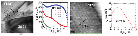
Figure 15. TEM image of the NEG-123 sample with 35 mol% Gd-211 and 0.1 mol% Nb2O5 (left); the critical current density performance for the same material around 77 K, H//c-axis (left, middle); STM image and critical current density for (Nd0.33Eu0.38Gd0.28)Ba2Cu3Oy with 5 mol% of 211 (right middle and right).
Download figure:
Standard image High-resolution imageA correlated pinning disorder originating from chemical composition variation in (Nd,Eu,Gd)Ba2Cu3Oy led to an enhancement of flux pinning at high magnetic fields. It manifested itself as a lamellar structure composed of clusters of a normal and NEG/Ba-rich material in the NEG-123 matrix (figure 15, middle right). The high magnification TEM and STM showed that the nano-twins are in fact planes composed of aligned clusters of 3–4 nm in size, aligned with and filling channels between regular twin boundaries. Such a new pinning structure led to a significant improvement of Birr up to 15 T at 77 K and H//c-axis [141, 142], which is the highest irreversibility field reported so far for high Tc superconductors at 77 K (figure 15, right). The most challenging task is to transfer this technology to the second generation of magnetically levitated vehicles (MAGLEVs), where operation cost reduction is highly demanded. For this purpose, it is necessary to push the technology further by fabricating good-quality large-size samples via batch production.
Advances in science and technology to meet the challenges.
Recent success in batch production of melt-textured LREBa2Cu3Oy superconductors has indicated the way to cost reduction in production of these materials. For a successful application of the bulk cuprate superconducting super-magnets the mechanical strength is also an important issue. The mechanical performance of the ceramic material has been improved by silver addition and by epoxy reign impregnation. As a result, these bulk magnets can survive at low temperatures and even a very high Lorenz force. During crystallographic transformation from non-superconducting tetragonal to the superconducting orthorhombic phase, a number of micro-cracks is formed in the lattice, especially in the (a,b)-plane direction. When the superconductor traps a high magnetic field, a large electromagnetic force acts on the material. As the cracks are the weakest spots of the lattice, there is the highest probability that just at the cracks the material will break. Epoxy resin can penetrate the cracks in the bulk superconductor so as the new class of superconducting super-magnets is able to trap magnetic fields as high as 17 T at 29 K (about 1.5 T at 77 K) without damage [144]. Taking advantage of the new technology, a compact, lightweight, and mobile permanent high-Tc magnet system was designed using the Gd-123 rings.
Another important application is in medicine; it is magnetic drug delivery system (MDDS) constructed and tested on rats and pigs with encouraging results. The drug delivery can be controlled by the superconducting magnetic force in the body and as a result, a high concentration of the drug is delivered to a targeted diseased tissue. In this way the drug toxicity to the normal tissue can be significantly reduced. The drugs delivery to the tissues located deep inside the body requires very strong small-size magnets. Only the superconducting ones can fulfil such a task. The industrial production of oxide superconductors already occurs, together with their first industrial applications. We believe that nano-structured cuprate superconducting super-magnets are able to open a new path for variety of industrial applications like MRI, NMR, drug-delivery systems in medical applications, water cleaning, space, railway, and naval transport systems, UPS systems etc.
Concluding remarks.
Nano-structured LRE-123 superconducting super-magnets are suitable for industrial super-magnet applications, capable of making rather dramatic changes in daily life. The technology opens the way for more practical, economical and reliable production, if we can find ways of how to control the matrix chemical ratio and/or the size and distribution of the initially added nano-meter size particles in the final compound. The high critical current density and irreversibility field at around liquid nitrogen temperature indicate that the nano-structured LRE-123 are the right materials for the next generation of superconducting super-magnets of top quality.
Acknowledgment.
The paper was supported by Grant-in-Aid FD research budget code: 112261, Shibaura Institute of Technology (SIT).
10. Silicon photonics enhanced with functional oxides: new opportunities
S Abel and J Fompeyrine
IBM Research GmbH, Säumerstrasse 4, CH-8803 Rüschlikon, Switzerland
Status.
Photonics is the backbone for high-speed internet across the world. In recent years, the need for bandwidth in servers drove the development towards a tighter integration of electro-optical systems. Silicon photonics is becoming the leading baseline technology for integrated optics, as CMOS was for integrated microelectronics. The key advantages of silicon photonics are low fabrication costs and reduced circuits' footprint, enabled by the large contrast in refractive index between SiO2 and Si. Alike CMOS, one can envision new materials as critical add-ons to the future of silicon photonics. Such materials will either enhance device performances, or enable functionalities that do not exist in silicon. For long range data communication, LiNbO3 modulators are the standard technology, albeit provided as discrete components. They demonstrate that functional oxide materials are already today crucial in photonics. Besides numerous properties that are appealing for real-world applications in the electrical domain, many oxides have also interesting optical characteristics. Their refractive indices can be altered by applying an electric, magnetic, thermal or mechanical strain field, as summarized in figure 16. This figure illustrates also that modulation, switching or optical isolation are essential functions when transceiving data between or on chip. In the following sections we present a short review of the state of the art for silicon photonics enhanced by functional oxides highlighting that optical properties in oxides can be mapped to specific functionalities in integrated optics.

Figure 16. (Left) Optical properties present in functional oxides that can potentially be exploited in the (upper right) optical data transmission chain implemented in (lower right) integrated photonics.
Download figure:
Standard image High-resolution imageCurrent and future challenges.
As of today, most of the challenges are related to the growth of materials with the appropriate optical properties, and to the methods required to integrate such materials with the silicon photonics baseline technology. For most of the properties highlighted in figure 16, the relevant optical characteristics are often tightly related to structural features. The Pockels effect describes for example the change of refractive index Δn for a material upon application of an electric field E,  . The Pockels coefficient 'r' vanishes for centro-symmetric crystals, and this effect is therefore only non-zero in materials whose crystalline structure is non-centrosymmetric, such as LiNbO3 or BaTiO3. Giant thermo-optic effects are also present in oxides that exhibit metal to insulator transition as a function of temperature. A large change in the real and imaginary part of the refractive index can be observed when the transition is crossed, such as in VO2 [145]. The transition is here directly correlated to a structural transition to a rutile phase, and can also be strongly impacted by lattice distortions [146], hence by the mechanical strain field in the films. Finally, magneto-optic effects can be exploited in materials with a strong Verdet constant, provided the crystal structure does not favor mixed valences that could translate in high optical losses. Growing thin films with the required structural and optical properties is therefore a challenging task, and an intense research is focusing on controlling intrinsic materials features. VO2 can for example be grown within a wide oxidation range, and its thermo-optical properties are dominated by the oxidation state, as well as by the dopants [147]. With the advent of new generic techniques to grow epitaxial perovskites on silicon, high quality BaTiO3 films can be grown on silicon and exhibit a strong Pockels effect [148]. In this case the epitaxial strain has a strong impact on the direction of the ferroelectric polarization, and the optical device design must take into account the microstructure [149]. For the integration of functional oxides with silicon photonics, two methods are explored, each having its specific challenges. First, direct growth on silicon can first be employed, using standard deposition methods. Besides the structural characteristics described previously, the films must also result in very low optical propagation losses when processed in waveguides. Recent reports have pointed out that propagation losses in BaTiO3 grown on silicon can be substantially reduced [150], with values of a few dB/cm within reach. Direct wafer bonding is however another promising approach, as it enables to optimize the oxide layer independently from integration aspects—including for its optical losses. This method has been successfully used to integrate LiNbO3 thin films onto silicon photonics circuits [151], as well as for magneto-optical devices based on garnets [152].
Advances in science and technology to meet challenges.
Once integrated in silicon, devices can be fabricated that exploit the oxide properties in silicon photonics devices. In the recent years, the potential of this approach has been demonstrated in various device types, as illustrated in figure 17. The phase transition of VO2 has been utilized in ultra-compact optical switches such as ring resonators with a diameter of 3 µm [153]. Broadband absorption switches have been demonstrated as well for 0.5 µm length, using the variation of the complex part of the refractive index in VO2. Such VO2/Si hybrid photonic devices are typically designed as standard silicon photonic structures that are locally covered with a thin VO2 layer. The interaction length is then restricted to a few µm, so that the insertion losses of the devices remain low, e.g. <2 dB. Recently, the demonstration of an electrically induced metal-to-insulator transition has been reported [154], opening the path to fully integrated electro-optical switches using VO2. Switching and modulation in active BaTiO3 devices has been also recently reported. Passive and active ring resonators and Mach–Zehnder modulators with a bandwidth of up to 5 GHz and 0.8 GHz, respectively, have been demonstrated [155, 156]. Remarkably, the corresponding effective Pockels coefficient in the BaTiO3 layer is almost an order of magnitude higher than in LiNbO3 modulators. Besides applications for high-speed switches, optical devices might also exploit the Pockels effect in very efficient, low-speed tuning elements which are necessary in highly scaled, resonant silicon photonic circuits. In [155] the resonance of a BaTiO3-based race track resonator could for example be tuned with only 4 µW nm−1. One of the current challenges in this field is to disentangle the contribution of physical effects intermixed with the Pockels effect, which is necessary to ultimately boost the bandwidth of the devices to 40 GHz and higher. Finally, integrated devices exploiting non-reciprocal light transmission have been also demonstrated [152]. Direct growth as well as wafer bonding on silicon waveguides have been achieved, mainly using garnets based on yttrium and iron. Although the figure of merit are moderate and quite strongly impacted by high propagation losses, this device demonstration nicely illustrates how the introduction of oxide-based materials enable functionalities that are complex to implement in silicon only.

Figure 17. Summary of device demonstration for (a) BaTiO3-based low-power tuning device, (b) BaTiO3-based high speed modulator (adapted from [156] with permission of OSA, The Optical Society), VO2-based electro-optic switch (adapted from [154] with permission of OSA, The Optical Society), YIG-based optical isolator (adapted from [152] with permission of NPG).
Download figure:
Standard image High-resolution imageConcluding remarks.
Together with the advent of integrated silicon photonics, the need to expand CMOS technology beyond its limit helped new deposition and integration techniques to emerge. This is in particular true for the science and technology of functional oxides: seminal works have been reported in the last years, where the unique optical properties of such materials are exploited in devices co-integrated within a silicon photonic platform. The primary field of applications remains centered on data communications. Nevertheless, having a technology like silicon photonics cross-fertilized with novel materials concepts, new research directions might arise in applications as different as quantum photonics, brain-inspired computing, or high-performance integrated sensors.
11. New oxide microcavities applications: from polariton lasers to fundamental physics at room-temperature
J Zuniga-Perez
CRHEA-CNRS, Rue Bernard Gregory, Sophia-Antipolis, 06560 Valbonne, France
Status.
If an emitter is embedded within an optical cavity and their interaction strength becomes larger than the interaction strength of the emitter and cavity modes with their respective environments, then the emitter-cavity system will enter the strong-coupling regime. The system can be no longer described in terms of independent emitter and cavity photon states, but rather in terms of mixed states: microcavity polaritons (polaritons, in the following). The recent interest in these quasi-particles arises from the combination of a particular energy dispersion, with a minimum at kparallel = 0, and the bosonic character of polaritons, which behave as bosons as far as excitons do so (i.e. below the Mott density). These two properties allowed the observation of Bose–Einstein condensation in a solid-state system, and the fabrication of a new type of lasers in which the gain mechanism is no longer stimulated photon emission but polariton scattering stimulated by final state occupancy. Interestingly, the operation temperature of these polariton lasers is limited by the temperature stability of the excitons. In this context, ZnO appears very appealing due to its 60 meV exciton binding energy, which assures exciton stability, and small Bohr radius <2 nm, which assures exciton bosonic behaviour up to large particle densities.
In recent years, the development of ZnO-based microcavities has enabled polariton lasing in planar microcavities, first at low temperature [157] and then at room-temperature [158], as well as the observation of polariton parametric scattering at room-temperature in ZnO microwires [159] (see figure 18). Furthermore, the large exciton-cavity photon interaction strength in some ZnO microcavities, characterized by Rabi energies in excess of 200 meV, has allowed to explore new types of condensates with excitonic fractions attaining 97% [160, 161], which are in general not accessible in other materials systems.

Figure 18. Scanning electron microscopy images of the two typical ZnO-based microcavities: planar, on the left, and microwire-based, on the right.
Download figure:
Standard image High-resolution imageCurrent and future challenges.
In spite of the recent realizations [158, 160], including the first hints for weak-lasing within a condensate of interacting bosons [161], ZnO is mostly considered as a material for applied polaritonics rather than for fundamental physics. There are probably two main reasons for this:
- 1.The polariton condensate 'checklist' has not been yet fully provided for the ZnO system: (i) extended spatial coherence—i.e. g1(r)—has been scarcely measured [160]; (ii) two-threshold behavior has never been reported; (iii) other footprints, such as the spontaneous spin symmetry breaking, have not been reported either. While there are already sufficient facts proving the polariton nature of the observed nonlinear emission [157–161], the aforementioned measurements in one and the same ZnO microcavity would close any further debate.
- 2.The fabrication of planar ZnO microcavities is much more complex and less controlled than that of GaAs-based microcavities, mainly due to the lack of ideal Bragg reflectors [157, 158, 162]. One might consider this argument equally valid for fundamental and for applied physics; however, the room-temperature operation argument is strong enough to prevail when devices are considered.
A most attractive option would be to combine fundamental and applied physics in existing ZnO microcavities. Indeed, many of these cavities, especially microwires, are multimode; therein, exciton resonances are coupled to several cavity modes, resulting in a ladder of polariton branches [158–161]. These cavities are, as illustrated in figure 19, perfect candidates for achieving parametric processes at room-temperature [159, 163] (e.g. for generation of entangled photons).

Figure 19. (a) Emission intensity below threshold measured at room-temperature along the thickness gradient in a fully-hybrid planar ZnO microcavity showing 4 lower polariton branches (the cavity thickness changes from 3λ/2 to 3λ). λ is the wavelength corresponding to the excitonic resonance, shown as solid line. (b) Fourier-space photoluminescence mapping of a ZnO microwire cavity under four different pumping powers. Reproduced with permission from [159], copyright 2012 by the American Physical Society.
Download figure:
Standard image High-resolution imageTo exploit these parametric processes it would be necessary to develop adapted spectroscopic techniques, which are common at telecommunication wavelengths but rare in the UV, as well as to improve microcavity fabrication. These advances should be accompanied by the possibility of polariton condensates (and polariton) manipulation, not only optically but also electrically, which would open definitively the doors for practical polariton-based ZnO devices [164].
Advances in science and technology to meet challenges.
In order to manipulate polaritons and polariton condensates, these should live as long as possible. Even if the last generation of planar ZnO microcavities display quality factors well above 1000 [158, 162], enabling to achieve polariton lasing at room-temperature, larger quality factors and more homogeneous photonic landscapes are necessary to ease polariton manipulation. If we refer to the more mature GaAs system, this means employing homoepitaxial ZnO-based distributed Bragg reflectors [165] with a large number of pairs (typically larger than 30), due to a reduced refractive index contrast; alternatively, new techniques for cavity report onto dielectric mirrors [158] would be extremely challenging but very rich in terms of future possibilities, since the fabrication of the active region and of the mirror would become completely decoupled.
Direct electrical injection of ZnO polariton lasers is for the moment unrealistic because of the difficulties in achieving reliable and large enough p-type doping. In this sense, any progress in developing p-type oxides compatible with ZnO, in particular with a suitable band alignment, would be a real breakthrough that would have an enormous impact. On the other hand, electrical manipulation of polaritons does not need such p-type material: in this case, the technological difficulty lies in the fabrication of electrical contacts sufficiently close to the microcavity active region without degrading its properties (neither the excitonic nor the photonic).
Concluding remarks.
The access to an unprecedented range of polaritons (from photonic to very massive ones) combined with room-temperature operation promise new discoveries and applications in ZnO-based polaritonics. Besides, new types of ZnO cavities increasing the richness of the topic can be already envisaged, either by extending the wavelength spectrum addressed by ZnO cavities [166] or by exploiting its piezoelectric character, which leads naturally to the field of cavity optomechanics.
12. Multiferroic bismuth ferrite
R Ramesh
Departments of Materials Science & Engineering and Physics, University of California, Berkeley, CA 94720, USA
Status.
Complex oxides present a broad range of interesting functionalities, such as high temperature superconductivity, colossal magnetoresistance, (anti-) ferromagnetic, (anti-) ferroelectric, piezoelectric and more recently multiferroic properties. BiFeO3 (BFO) is the only room temperature multiferroic (antiferromagnetic and ferroelectric) so far, which has attracted great interest and extensive investigation in the past decade. It has a rhombohedral unit cell, built with two distorted perovskite cells connected along a pseudocubic [1 1 1] direction [167, 168]. It is also a G-type antiferromagnet with Neél temperature of ~673 K [1 0 0] and a symmetry-allowed, small canted moment due to the Dzyaloshinskii–Moriya interaction [169]. The hybridization between the two 6s electrons in Bi [170] with surrounding oxygen ions leads to a large displacement of the Bi cations relative to the oxygen octahedral along the [1 1 1] direction with a Curie temperature of 1103 K and the spontaneous ferroelectric polarization of about 90 µC cm−2 [171].
The synthesis of high quality epitaxial thin films through a variety of techniques (pulsed laser deposition (or laser MBE), sputtering, MBE, CVD) has already been well-established [172]. In thin films, both 71° and 109° domain walls are observed. Figure 20 shows the magneto-transport behavior of 109° domain walls, an atomic resolution image of which is shown in figure 20(a). Conducting atomic force microscopy (AFM) based measurements, figure 20(b), show that the walls are less resistive, (compared to the domain itself) typically by 2–3 orders of magnitude [173]. Macroscopic magneto- transport studies, Figures 20(c) and (d) show the existence of a large magnetoresistance when the transport direction and magnetic field direction coincide along the wall plane. Low temperature magnetotransport data, figure 20(d), shows a positive temperature coefficient, i.e. it decreases with decreasing temperature. It would be fascinating to study the possible emergence of metallic behavior at the domain walls, a grand challenge for the field of complex oxides [174]. Large compressive epitaxial constraint induces a phase transition to a super-tetragonal phase. Partial relaxation of the epitaxial constraint by increasing the film thickness leads to the formation of a mixed phase nanostructure which exhibits the coexistence of both the R- and T-phases. The highly distorted R-phase in this ensemble, shows a significantly enhanced ferromagnetism. These observations raise several questions: (i) first, what is the magnetic state of the strained R-phase? Given that spin-orbit coupling is the source of the canted moment in the bulk of BFO, can this enhanced moment be explained based on the strain and confinement imposed on the R-phase? What is the state of the Dzyalozhinski–Moriya vector in such a strained system? Are there other pathways to enhance the canted moment arising from D–M interactions, perhaps through engineering the crystal symmetry of BiFeO3? If yes, does this also present a pathway to switch the magnetic state with the application of a magnetic field?
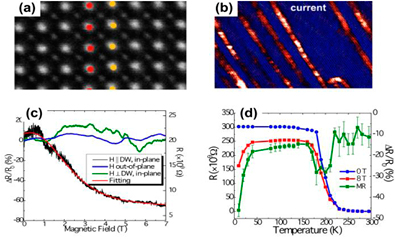
Figure 20. (a) An atomic resolution TEM image of the 109° domain wall; (b) conducting AFM image of transport through such domain walls; (c) macroscopic magnetotransport data through an array of 109° walls showing the significant MR for transport and H parallel to the wall while transport and/or H normal to the wall shows very little MR; (d) temperature dependence of the resistance and MR behavior.
Download figure:
Standard image High-resolution imageElectric field control of ferromagnetism is the most exciting development, figure 21. Element specific x-ray spectromicroscopy, magnetotransport and scanning electron microscopy polarization analysis has demonstrated the direct coupling between the canted moment in a domain and the moment in the CoFe ferromagnet [175, 176]. Figure 21: The coupling between a CoFe layer (FM) and the BFO can be probed using a standard spin valve like structure, shown schematically in (A); the corresponding schematic of the exchange coupling at the CoFe–BFO interface is shown in (B). Figure 21(C) illustrates the essence of the coupling studies. In red is the ferroelectric hysteresis, while the blue data is the resistance modulation of the spin valve with an electric field. For comparison, the magnetic field dependent modulation of the spin valve resistance is shown in (D). There are ample opportunities to improve on this. First, switching from a spin valve to a tunnel junction will yield at least an order of magnitude improvement of the resistance modulation. It would be extremely valuable to study approaches to grow out-of-plane magnetized ferromagnets and tunnel junctions on the BFO.
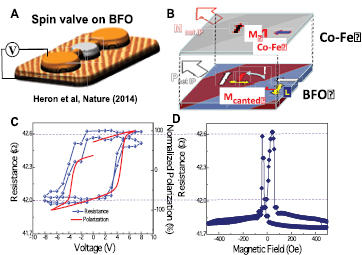
Figure 21. (A) A schematic of the spin valve test structure on BFO; (B) a schematic of the exchange coupling at the CoFe–BFO interface; (C) ferroelectric hysteresis (red) and MR hysteresis (blue) of the spin valve; (D) the corresponding R–H plot of the spin valve.
Download figure:
Standard image High-resolution imageCurrent and future challenges.
The field of multiferroics and magnetoelectrics is poised for some exciting times in the next 5–10 years. While a significant amount of fundamental understanding has been gained, it is now time for these scientific discoveries to be translated into the first stage of technological applications. Indeed, this could be said of the entire field of oxide electronics, where the science has always been well ahead of the technological implementations. If a room temperature multiferroic with a spontaneous magnetic moment (canted or otherwise) that is an order of magnitude higher than that in BFO, then this would be a game changer. There is quite a bit of worldwide effort focused on this. In the meantime, a focused effort on using exchange or strain coupled heterostructures may be the most available pathway to demonstrate devices. Perhaps the biggest focus area has to be low power electronics, since this is the most important advantage of going to electric fields compared to magnetic fields. At a higher level, it is important to explore new device concepts as well as new product markets that take advantage of the coupling between electricity and magnetism.
13. Novel functionalities at oxide (multi)ferroic domain walls
Nicola A Spaldin
Materials Theory, ETH Zurich, Wolfgang-Pauli-Strasse 27, 8093 Zürich, Switzerland
There has been tremendous interest recently in interfaces between insulating oxides with different electrical polarizations, in which electrostatic stability requires screening of the so-called polar discontinuity by either free or bound charge. The resulting accumulation of carriers in a narrow almost 2D region has been associated with a range of phenomena, including electrical conductivity, magnetism and even superconductivity (for a review see [177]). In most cases, such interfaces are engineered using layer-by-layer growth of two different materials, and the location of the screening layer is therefore fixed statically within the material. Particularly exciting, and to date less well studied, are polar discontinuities generated at ferroelectric domain walls through head-to-head or tail-to-tail components of the ferroelectric polarization. In this case, all of the physics of a static discontinuous polar interface is captured, with the additional desirable feature that the position of a ferroelectric domain wall can be changed using an applied electric field. Here we review the progress in this area to date, mention some other novel functionalities at ferroic and multiferroic domain walls, and discuss likely future directions.
Status.
The first observation of room temperature electrical conductivity in a ferroelectric domain wall occurred in thin films of the prototypical multiferroic, BiFeO3 [178]. The original data is reproduced in figure 22. Ferroelectric domains were written and imaged using piezoforce microscopy (PFM), and local conductivity was measured using high-resolution conductive atomic force microscopy (c-AFM). Conductivity was observed at 180° and 109° domain walls and associated with an electrostatic potential step accompanied by a change in band gap across the wall; subsequently the 71° domain walls were also shown to be conducting [179]. Clever patterning of domain walls of various orientations in BiFeO3 using scanning probe microscopy techniques later proved that the accumulation of carriers is indeed governed by the magnitude of the polar discontinuity at the wall, and demonstrated that this polar discontinuity can be tuned dynamically [180].
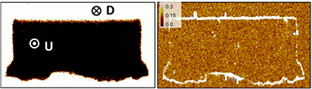
Figure 22. First observation of conducting ferroelectric domain walls in a multiferroic material. Left: out-of-plane piezoforce microscopy image of a written domain pattern in a monodomain BiFeO3 film, showing up (U) and down (D) components of ferroelectric polarization. Right: corresponding conducting atomic force microscopy image showing conduction at the domain walls. The scale bar is in picoamperes. From [178], reproduced with permission.
Download figure:
Standard image High-resolution imageA particularly interesting development was the report of conductivity at the ferroelectric domain walls in the multiferroic hexagonal manganites [181]. Here the improper nature of the ferroelectricity leads naturally to a domain structure with coexisting neutral, head-to-head and tail-to-tail walls. The authors showed that the electrical conductance in hexagonal ErMnO3 varies continuously with the domain wall orientation, with the tail-to-tail walls, which are screened by the accumulation of positive charge, having the highest conductivity in this p-type material.
While the phenomenon of electrically conducting ferroelectric domain walls was at first believed to be a property of multiferroics, it was soon after demonstrated in the conventional ferroelectrics lead zirconium titanate (PZT) [182] and BaTiO3 [183]. In the PZT case, the walls were nominally neutral with no polar discontinuity, although high-resolution transmission electron microscopy indicated many small steps which would require local screening. In the BaTiO3 example, head-to-head and tail-to-tail walls were created by so-called frustrated poling, and stabilized by the combined availability of free carriers and coupled ferroelastic clamping.
Additional evidence of the importance of the interaction between ferroelectric domain walls, defects and clamping was provided by an intriguing study of the relationship between domain walls and conductivity in strained multiferroic strontium manganite, SrMnO3 [184]. First, the theoretically predicted ferroelectric polarization in tensile-strained films of SrMnO3 was confirmed using second harmonic generation (SHG). Electrostatic force microscopy then revealed an unexpected behavior: The ferroelectric domains were found to form discrete chargeable nanodomains with distinct conductances (figure 23). A model was proposed in which oxygen vacancies, which are stabilized by the tensile strain, accumulate at the domain walls and create a potential barrier to charge transport between the domains.
Figure 23. Normalized conductance of a multiferroic SrMnO3 film measured using electrostatic force microscopy. The degree of brightness indicates the conductance of each stripe-like ferroelectic domain. The scale bar is 0.5 µm. From [184], reproduced with permission.
Download figure:
Standard image High-resolution imageWhile the focus of this short road map is on electrical conductivity at ferroelectric domain walls, we mention that other intriguing properties have been reported at the domain walls in various ferroic systems, including a net magnetism at the ferroelectric domain walls in otherwise antiferromagnetic multiferroic BiFeO3 and (my personal favourite) the occurrence of BCS superconductivity at the ferroelastic twin boundaries in Na-doped WO3 [174]. (For a review of other functionalities see [177].) While simple model explanations exist—the superconductivity is likely due to the higher concentration of carriers compared with the bulk sample, and the net magnetism is likely related to changes in structure and bonding at the interface—the details of these and related phenomena remain to be fully understood.
Current and future challenges, and advances required to meet them.
Much remains to be understood mechanistically regarding the nature and origin of electrical conductivity at multiferroic domain walls. Here a combination of first- principles and phenomenological theories with a wide range of detailed and careful characterization tools addressing different time- and length-scales will be required for progress. In particular, the interplay between the detailed atomic structure of the walls, the screening of associated internal electric fields with minority or majority free carriers and/or bound charge, and the role of ionic point defects still remain to be elucidated. None of these properties can be measured straightforwardly, with characterization of point defects such as oxygen vacancies being particularly challenging. Electronic structure calculations for domain walls are also not routine due to both the computational demands of the large supercells required to model realistic domain wall spacings and defect profiles, and the state-of-the art methods required to appropriately incorporate physically meaningful electrostatic boundary conditions. The material chemistries and crystal structures that have been explored to date remain rather limited, and doubtless new behaviours, as well as clarifications of existing ones, will be achieved when a broader chemical and structural palette is explored. Regarding potential for devices, while it is hard to be predictive, such sub-nanometre sized, electrically tunable, conducting entities are certainly seductive. For consideration for practical applications there are two outstanding challenges: An increased current density at the walls—perhaps even demonstration of a metal–insulator transition—should be achieved, as well as a route to controlled manipulation of their position.
Concluding remarks.
Novel and emergent properties at ferroelectric and multiferroic domain walls offer arguably one of the most interesting new research directions in the field of complex oxides and will undoubtedly continue to be actively pursued in the next years. While a direct route to applications is not yet entirely clear, the technological potential is huge, and provides an additional driver for progress, in addition to the desire to understand the intriguing fundamental physics.
14. Switchable 2D electron gas at the multiferroic interfaces
Sergey Ostanin, Vladislav Borisov and Ingrid Mertig
Institute of Physics, Martin Luther University Halle-Wittenberg, Von-Seckendorff-Platz 1, 06099 Halle, Germany
Status.
Surprisingly, a 2D electron gas (2DEG) can appear at the interface between robustly insulating oxides. This fascinating phenomenon, which was first observed [73, 185, 186] in LaAlO3/SrTiO3 (LAO/STO), is attributed usually to its LaO/TiO2-terminated (0 0 1) perovskite interface. To explain the emerged 2DEG the researches, assuming mostly that the interface is perfect and stepless, invoke the arguments related to the issue of polar catastrophe. Since LAO (0 0 1) represents alternately charged planes [LaO]+ and [AlO2]−, each interfacial La transfers ½ electron into the next and formally neutral TiO2-layer of STO. Therefore, the oxidation state of interfacial Ti decreases. This scenario for the Ti3.5+ valence state and corresponding d-orbital reconstruction, which results in 2DEG at the LaO/TiO2 interface, was modeled [187] from first principles. However, all epitaxially grown oxide heterostructures contain intrinsic imperfections, such as oxygen vacancies and substitutional intermixing of cations across the interface. Each type of these interfacial defects causes additional charged carriers, namely, electrons for oxygen vacancies and holes for the Sr substitutes [188, 189]. Thus, both of these defect-based mechanisms contribute to the 2DEG effect as well but mediate it differently. For instance, the Sr/La intermixing >30% completely destroys the 2DEG. There is a family of composite perovskites for which the LaO/TiO2 termination is formed unavoidably. In particular, 2DEG can appear between STO (0 0 1) and LaFeO3 (LFO). Recently, Li et al [190] have reported that the crystalline and partially amorphous ABO3/STO (A = La, Pr, Nd and B = Al, Ga) interfaces become conducting for ABO3 thicker than 4 unit cells (u.c.). High crystallinity of the interface is crucial for the polar catastrophe mechanism of 2DEG. After oxygen annealing (when the O redox mechanism is removed) the interfaces prepared at 500 °C and below become insulating while samples prepared at 515 °C and above are conducting [190]. In the context of the underlying 2DEG mechanisms and their interplay, the ab initio calculation show that, with increasing amount of interfacial defects for each of the Sr substitutes and O vacancies, these two mechanisms act oppositely.
Current and future challenges.
Presently, the focus of discussions around the 2DEG shifts gradually toward its functionality and switchability. Here, the so-called multiferroic TiO2-based interfaces seem very promising. When the STO component of the composite system is replaced by a robust ferroelectric (FE), such as BaTiO3 (BTO), this may create an extra functionality due to its switchable polarization. Indeed, the LAO/BTO heterostructure was fabricated already [191]. On the other hand, when LAO is replaced by a magnetically ordered perovskite, this allows to change the magnetization, M, of magnetic side by the BTO polarization reversal. The change of M is crudely estimated using the coercive field Ec [192]: ΔM ~ αEc, where α is the magnetoelectric coupling coefficient. Meanwhile, among all magnetically ordered cubic perovskites ABO3, the overwhelming majority are antiferromagnetic (AFM) and insulating. Some of them are in a good lattice match with FEs and, therefore, the AFM/FE oxide interfaces can be grown epitaxially. For instance, LFO/PbTiO3 is a good candidate for externally tuned 2DEG. It should be noted that manipulation with the FE polarization along [0 0 1] is not trivial. Robustly switchable epitaxial FEs are thicker than 5 u.c. and since they grow in complete unit cells, their surface termination and interfacial composition are correlated. Hence, the target TiO2-terminated interface of FE means that the other termination or surface is AO-terminated. Until now, it is not clear whether the depolarization field coming from the surface affects the ferroelectrically driven 2DEG. Regarding the AFM side, its thickness-dependent scenario of the 2DEG as well as the role of its interfacial defects need a careful study. A critical limitation for the gap width in AFMs, compared to that of the wide gap FEs, is an open question so far.
Advances in science and technology to meet challenges.
The density functional theory suggests that the 2DEG emerged at the multiferroic interface may occur with no defects and, moreover, without La species. This has been anticipated [193] from first principles by combining BTO and the G-type AFM insulator, SrTcO3 (STcO), which possesses the orthorhombically distorted perovskite structure and whose lattice mismatch with BTO (0 0 1) is <1%. Since the experimental gap of STcO is not available, this value was modeled between 0.5 eV and 3 eV, using the Hubbard parametrization. Two types of terminations of BTO/STcO, i.e. BaO/TcO2 and TiO2/SrO as shown in figure 24, were simulated using superlattice geometry and a supercell with vacuum, which both mimic differently the electrostatic boundary conditions. The interatomic force minimization results in the ionic displacements near the interfaces, which change locally the FE and magnetic properties so that the system screens off the chemical potential mismatch between the two materials.

Figure 24. The layer-resolved energy positions of the valence and conduction bands, calculated for each termination of BTO/STcO and for dually polar BTO. The hole (electron) charge carriers induced in the band gap are shown by red (blue) shaded area.
Download figure:
Standard image High-resolution imageUsing the site-projected density of states (DOS), calculated for each atomic layer of BTO/STcO, one can disclose [193] how the valence- and conduction-band edges vary toward the interface and how the electron (hole) carriers appear in the gap, within few interfacial u.c., as shown in figure 24. Then, by integrating the DOS tails occurring in the gap, the induced charges, their electron (hole) character and spin polarization were evaluated. For each termination, the character of the 2DEG carriers changes from electrons to holes upon the polarization reversal. This conclusive theoretical result weakly depends on the optionally used electrostatic boundary conditions, the film thickness and degree of electronic correlations. The 2DEG effect, which is controlled by the FE state of BTO, is anticipated for the defect-free and atomically sharp interfaces of BTO/STcO.
Concluding remarks.
Multiferroic interfaces between the FE and AFM insulating perovskites, as the contemporary theory suggests, may form such 2DEG, for which the charge character of ferroelectrically induced carriers changes from the p- to n-type by the polarization reversal. The effect should robustly appear at the perfect interface even if the defect-based mechanisms of 2DEG, originated due to the interfacial cation mixing, oxygen vacancies and interstitial species, were excluded from consideration. The dominant mechanism of ferroelectrically driven 2DEG is the electron/hole transfer that goes so that charged carries are accumulated near the interface, within a few layers. When BTO is forced to be paraelectric the effect disappears. This suggests another scenario of a thermally driven 2DEG, which can be switched on and off. Thus, the FE/AFM interfaces offer extremely promising applications. Until now, the theory is not able (i) to suggest the voltage needed for the FE switch of 2DEG and also (ii) to claim which polarization state of BTO is initially formed under the non-equilibrium growth conditions. Nevertheless, these findings could stimulate further studies, which include the effect of spin-orbit coupling in non-centrosymmetric composite oxides.
Acknowledgement.
This work was supported by Sonderforschungsbereich SFB 762, 'Functionality of Oxide Interfaces'.
15. Magnetoelectric coupling in multiferroic epitaxial thin film composites
Vera Lazenka1, Michael Lorenz2
1 KU Leuven, Leuven, Belgium
2 Universität Leipzig, Leipzig, Germany
Status.
Recent progress in materials science and technology and the hope for realization of novel device functionalities has renewed research interest in multiferroic and magnetoelectric materials [194, 195]. In particular, complex oxide heterostructures offer the possibility to realize next generation electronics, such as novel data storage devices [195]. Magnetoelectric multiferroic composites consisting of several closely coupled phases show advantages compared to single-phase magnetoelectrics in terms of value of magnetoelectric coefficient, control of its temperature dependence, and design of tailored materials for applications [194–198]. Important for applications is the strength of magnetoelectric coupling. The linear and nonlinear coupling coefficients in single phase magnetoelectrics are usually low [194]. However, indirect coupling due to strain effects, i.e. inclusion of piezomagnetism and magnetostriction, or piezoelectricity and electrostriction, can be orders of magnitude higher in two-phase composite materials [194]. Because not only the elastic coupling at the interface, but also exchange-bias effects, or modulation of the charge carrier concentrations can mediate the indirect magnetoelectric coupling, its distinct identification in multiphase composites is a matter of current research [195].
Among the possible composite geometries of the coupled phases, the multilayer structure, i.e. a so called 2-2 composite consisting of pairs of 2D stacked layers, is expected to be far superior to bulk composites. This is because out-of-plane leakage currents in the low-resistive ferromagnetic phase are considerably reduced, and because piezoelectric thin layers can be easily and almost homogeneously poled electrically [196]. Both effects may enhance the magnetoelectric coupling in superlattice composites by orders of magnitude. Vaz pointed out, that magnetoelectric coupling in composites is interfacial in origin, and that the three different, above mentioned mediation types elastic strain, charge, and exchange bias provide different characteristic responses and functionalities [197].
Among the many possible combinations of ferroelectric, ferromagnetic, or multiferroic materials in composites, the BiFeO3–BaTiO3 solid solution is mentioned as 'highly exciting towards the realization of a room temperature single phase multiferroic magnetoelectric material', as pointed out by Priya et al in [198](p 103 ff). In order to further illustrate the current status of magnetoelectric composites with special emphasis on epitaxial BaTiO3–BiFeO3 superlattices, we show in the following recent examples how to correlate the magnetoelectric voltage coefficient αME with microstructural features and the magnetic spin structure. Figure 25 shows the temperature-dependent αME of two epitaxial BaTiO3–BiFeO3 thin film superlattices, and illustrates the chemical and structural homogeneity of the well ordered high-αME sample grown at 0.25 mbar with atomically smooth, coherent interfaces [199–201]. The (linear) magnetoelectric voltage coefficient αME was determined using an inductive AC-method by αME = dV/(tdH), where V is the voltage induced by the exciting AC magnetic field H, and t is the thickness of the sample, see [199–201] and references therein. Up to now, the highest magnetoelectric voltage coefficient of 49 V cm−1 Oe−1 at 300 K and 1 kHz has been reached in a multiferroic (BaTiO3–BiFeO3) × 15 superlattice with total thickness of 208 nm, which is correlated to atomically coherent interfaces, see figure 25 and [201].

Figure 25. (a) Temperature dependent magnetoelectric (ME) voltage coefficient of two (BaTiO3–BiFeO3) × 15 superlattices grown at the indicated oxygen partial pressures with pulsed laser deposition on SrTiO3 (0 0 1). (b) HAADF and EDXS maps of Ba, O and Bi of a typical (BaTiO3–BiFeO3) × 15 superlattice grown at 0.25 mbar with state-of-the-art magnetoelectric coefficient. Note that the SrTiO3 substrate is on top in the images in (b). The Ti and Fe maps (not shown) are similar to that of Ba and Bi, respectively. The scale bar is 60 nm. (c) HR-TEM image of the supperlattice from (b), demonstrating the coherent and strain-free growth of the layers near the surface of the high-αME superlattice. Images adopted with permission from [201].
Download figure:
Standard image High-resolution imageSimilarly high αME of 43 V cm−1 Oe−1 at 300 K was obtained in a series of chemically homogenous 67% BaTiO3–33% BiFeO3 composite films [202]. In comparison, a ceramic BiFeO3 bulk sample showed only αME = 7.1 mV cm−1 Oe−1, and a slightly higher value of 9.15 mV cm−1 Oe−1 was achieved in a Bi0.8Gd0.2FeO3 bulk sample. Epitaxial single-phase BiFeO3 films show αME = 2–4 V cm−1 Oe−1. At the same time, the BaTiO3–CoFe2O4 nanocomposite system, consisting of CoFe2O4 nanowires in a BaTiO3 matrix, showed a αME around 80 mV cm−1 Oe−1, in agreement with values published by Ramesh et al, see [202]. As a proof of the reliability of the used magnetoelectric measurement setup, the αME coefficient measured across a non-magnetoelectric Fe (5 nm)–LiNbO3 (100 µm) heterostructure amounted only 0.05 mV cm−1 Oe−1.
Current and future challenges.
Not well understood are the different temperature and DC magnetic field dependences of the magnetoelectric voltage coefficients of BaTiO3–BiFeO3 superlattices and homogeneous composite films, see figures 25 and 26, and [199–202]. In a first attempt, we were able to correlate the αME values of the superlattices with density of oxygen vacancies and antiphase octahedral rotations [199]. Interestingly, interface-engineered oxygen octahedral coupling was recently used to manipulate the magnetic and electronic anisotropy in manganite heterostructures, see [276]. Moreover, the magnetic spin structure was found to affect the characteristics of αME in an external magnetic field [200]. Detailed investigation of the microscopic strain in multiferroic superlattices requires high-resolution TEM investigations, as shown in [201]. In the homogeneous BaTiO3–BiFeO3 composite films, the magnetoelectric coupling seems to be correlated to an oxygen vacancy superstructure [202]. The temperature dependence of αME of the homogeneous composite films is opposite to that of the superlattices, so that strain-mediated coupling alone cannot explain its origin [202]. Probably, charge-mediated magnetoelectric coupling may be important additionally [202, 203].
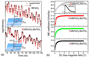
Figure 26. (a) Nuclear forward scattering time spectra of a BiFeO3 thin film and a (BaTiO3/BiFeO3) × 15 multilayer. The spectra were recorded at room temperature and zero external magnetic field. The solid lines are the model fits of the spectra. The insets in (a) are schematic representations of the fitting model for the thin film and the multilayer.  is the magnetic moment of the BiFeO3 layer(s) and
  is the wave vector along the photon beam. Figures reprinted from [200] with the permission on AIP Publishing. (b) Magnetoelectric (ME) coefficient as a function of DC bias magnetic field at 300 K for the BiFeO3–BaTiO3 multilayers with the indicated number of double layers from 2 to 20. The inset in (b) is αME of a single phase BiFeO3 thin film for comparison. It shows different characteristics.
Download figure:
Standard image High-resolution imageAdvances in science and technology to meet challenges.
In addition to the above mentioned microstructural methods, nuclear forward scattering of synchrotron radiation is an ideal approach to access the local magnetic spin structure on the nanoscale. The measured scattering spectra for a BiFeO3 thin film and a (BaTiO3–BiFeO3) × 15 multilayer together with the fits are presented in figure 26(a). The fits show a spin reorientation in the highly strained BiFeO3 layers within the multilayer compared to the single film, see insets of figure 26(a) [200]. We correlate the enhanced magnetic and magnetoelectric properties observed in the multilayers with the suppression of the spiral spin magnetic structure which is due to high epitaxial strain in the multilayer and interfacial interaction between ferroelectric BaTiO3 and multiferroic BiFeO3 [200]. In our latest work we show the tunability of the magnetization and of magnetoelectric coefficient in the multilayered BaTiO3–BiFeO3 system by varying the number of interfaces. A nearly perpendicularly magnetized multilayer with 20 layer pairs was fabricated that shows the highest value of magnetoelectric coefficient in this series of superlattices, see figure 26(b).
Concluding remarks.
With the knowledge about magnetoelectric coupling mechanisms and the correlation to the particular microstructure and magnetic spin structure a design of novel artificial thin film composites will be possible. Tailored coupling parameters could meet the requirements for future applications in magnetoelectric sensors and memories [198, 203].
Acknowledgements.
We acknowledge financial support of the Deutsche Forschungsgemeinschaft (DFG) within SFB 762 'Functionality of Oxide Interfaces', and of the Fund for Scientific Research—Flandern (FWO) and the KU Leuven Concerted Action (GOA 14/007).
16. Self-assembled multiferroic nanocomposites
G Srinivasan
Physics Department, Oakland University, Rochester, MI 48309, USA
Status.
Multiferroic materials that exhibit two or more of the primary ferroic properties (ferromagnetism, ferroelectricity, ferroelasticity) have been of interests in recent years. A composite made of a ferromagnetic and ferroelectric phases is an engineered multiferroic in which coupling between the ferroic phases could occur through a variety of mechanisms including transfer of strain, charge, or spin torque at the interface. Our focus here is on strain mediated magneto-electric (ME) coupling in the composites and is defined as induced polarization in an applied magnetic field (direct ME effect) or an induced magnetization (or anisotropy field) in an electric field (converse ME effect) [204, 205]. Strong ME coupling was reported in oxide composites with ferrimagnetic spinel and hexagonal ferrites or ferromagnetic manganites and ferroelectrics such as barium titanate (BTO), lead zirconate titanate (PZT), and lead magnesium niobate-lead titanate. Efforts so far on the multiferroic composites have focused on the nature of ME coupling at low-frequencies and at mechanical resonance modes and applications such as magnetic sensors, tunable inductors and capacitors, dual electric and magnetic-field tunable signal processing devices such as resonators, filters, and phase shifters for use at 1–110 GHz, in energy harvesting, solar cells, and random access memories [204, 205].
Current and future challenges.
The strength of strain mediated ME interactions is expected to be strong in nanocomposites due to a surface-to-volume ratio that is a factor of 103 to 106 higher than for thin film composites in which substrate clamping weakens the ME coupling. Such clamping can be easily overcome in nanopillars in a host matrix, core-shell fibers and core-shell particles [206–209]. Synthesis of nanopillars of ferrites in BTO, PZT or BiFeO3 matrix was reported by several techniques including pulsed laser deposition [209]. Ferrite-ferroelectric core–shells nanotubes were synthesized on porous anodized aluminum oxide (AAO) or membrane templates by a combined sol–gel and electrochemical deposition technique [204, 205]. The use of electrospinning was reported for core-shell fiber synthesis [207]. The technique utilizes electrical forces to produce fibers of diameters in the range 100 to 1000 nm (figures 27(a) and (b)). Synthesis of core–shell particles of ferrite and BTO or PZT by techniques including surfactant-assisted thermal method and by hydrothermal annealing process were reported. In recent studies particles of BTO and spinel ferrite were functionalized by attaching complementary coupling groups and a core-shell particulate composite (figures 27(c) and (d)) was formed by covalent bonds between the two particles with the addition of a coupling agent [208, 209].
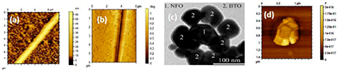
Figure 27. (a) AFM topography and (b) scanning microwave microscopy (SMM) phase images for fibers of nickel ferrite (NFO) core and PZT shell made by electrospinning. (c) SEM and SMM images for a particle with NFO core and BTO shell synthesized by chemical assembly. (d) SMM capacitance image for NFO core-BTO shell particle.
Download figure:
Standard image High-resolution imageAlthough nm-scale multiferroic oxide composites with core–shell structures have been synthesized and characterized in recent years [207–209], further assembly of nanomaterials to well-ordered mm-size superstructures is of importance for applications in useful technologies [212]. Traditional lithography techniques are not viable for fabricating mm-size structures with nm-periodicity [211, 212]. Assuming an assembly rate of 103 s−1, for example, would require 16 min for a 103 × 103 2D planar array of unit blocks and nearly 300 h for a 103 × 103 × 103 array. Chemical and DNA/RNA assisted self-assembly and external stimuli such as magnetic and electric fields for instantaneous assembly are of interest in this regard [208–210]. Modeling efforts on such self-assembly techniques and theory of ME coupling in assembled superstructures are lacking at present. It is necessary to consider the electric and magnetic dipole-dipole interactions in modeling the assemblies and for theory of low-frequency ME effects and coupling at individual and collective resonance modes of the composites. Similarly for modeling ME coupling at ferromagnetic and magneto-acoustic resonances one has to develop theory of magnetic modes in assemblies [204].
Advances in science and technology to meet challenges.
Focused efforts are essential on assembly of the nanomaterial into superstructures with strong ME coupling at low-frequencies and at resonance modes. Recent studies on chemical-, DNA-assisted, and magnetic and electric field-directed assembly techniques are noteworthy in this regard. (i) Chemical assembly: core–shell nanoparticles of NFO and BTO were assembled by attaching complementary chemical groups, azide and alkyne, to the particles and then assembling them by Cu(I)-assisted click-reaction [207]. Studies by SEM and scanning microwave microscopy (SMM) at 1–26 GHz showed the core-shell structures with well-defined interfaces (figure 27). Evidence for strong ME coupling was observed through magnetic field induced polarization and magneto-dielectric effects. (ii) DNA-assisted assembly: a 'click' methodology was used to covalently attach alkyne functionalized oligomeric DNA (ODN) to azide-functionalized nanoparticles and fibers. The ODN groups allowed for specific reversible DNA-DNA hybridization for the formation of core-shell particles, PZT fiber coated with ferrite particles, and bundles of core–shell nanowires [213]. Figures 28(a) and (b) show SEM and SMM images of DNA-assembled NFO–BTO core–shell particles. Although employment of DNA as a linker has been reported for nanoparticle assembly, essentially no work has been reported using RNA [207, 210]. Like DNA, RNA can base-pair with complimentary RNA (or DNA) with the additional ability of base-pairing with complimentary sequences on the same strand. It is expected that RNA will have slightly weaker binding characteristics than DNA thus allowing for lower melting temperatures used in restructuring morphologies. The ability to custom synthesize DNA and RNA with 100 or greater nucleotides, provides us with a wide range of possibilities for controlling the interaction strength and specificity between nanoparticles, leading to superior control in generating macrostructures.

Figure 28. (a) SEM and (b) SMM images for DNA-assembled NFO shell-BTO core particle. (c) and (d) SEM images for superstructures of NFO-BTO core-shell particles assembled in a uniform and rotating magnetic fields, respectively.
Download figure:
Standard image High-resolution imageBuilding blocks of core-shell particles and coaxial fibers could be assembled in uniform or nonuniform magnetic fields H and in DC or AC electric fields E ([207, 213] and references therein). Models predict the assembly to result in a variety of superstructures, such as rings, chains, bundles, and arrays due to magnetic dipole moment and electric polarization associated with the nanostructures. In the case of H-directed assembly one could apply either a uniform field or a field gradient [214]. Under a uniform field H (at angles other than 0 or 180°) a magnetic moment will be subjected to a torque that aligns the moment along H. A field gradient, however, exerts an attractive force on the moment associated with a particle or fiber and moves and aligns them in the regions of high field strengths. As the assembly proceeds, magnetic dipole moment of fibers will create a nonuniform field and exerts a force on neighboring nanostructures leading to local variation in the assembly symmetry. For modeling H-driven assembly, it is necessary consider the influence of magnetic moment, size and shape of the nanostructures.
The assembly of a nanomaterial in an AC electric field is due to dielectrophoresis, i.e. motion of a high aspect ratio nanoparticle due to induced polarization in E. The techniques has been successfully used for alignment and assembly of conducting, semiconducting and nonconducting nanowires and particles [215]. Although the assembly is usually done in an AC field with the speed of assembly and resulting configuration are dependent on the strength and frequency of the AC field, dielectrophoresis was reported in DC fields as well. In some studies a combined AC and DC electric fields and AC E-field and static H-field were used for orienting nanostructures and for their assembly. The superstructures could also be assembled in crossed E and H-fields that offers enhanced flexibility in types of assembled structure.
Concluding remarks.
Composite multiferroics are of fundamental and technological importance. The strain mediated coupling is expected to be much stronger in nanocomposites than in thin film structures. It is however necessary to assemble superstructures of such nanomaterials for basic studies on ME coupling and for a variety of applications. Several viable paths for instantaneous assembly of the nanocomposites have been discussed here. We anticipate new phenomena, theory and novel applications to emerge from this research.
Acknowledgement.
GS is supported by grants from the Army Research office, the National Science Foundation and DARPA.
17. Combinatorial substrate epitaxy: a novel approach of epitaxy for oxide films
Wilfrid Prellier
Laboratoire CRISMAT, ENSICAEN, CNRS UMR 6508, 6 Boulevard Maréchal Juin, 14050 Caen, France
Status.
Transition-metal oxides attract attention because of their fascinating properties, including superconductivity, magnetism, ferroelectricity or insulator-to-metal transitions. There has been a growing activity in the development of thin film transition metal oxides because of their relevance to device applications, because properties can be modified owing to thin film strains, especially epitaxial coherency strains. As a consequence, metastable polymorphs/phase arrangements with novel physical properties have been fabricated as thin films. Reducing the thickness of the layer down to a few unit cells is also interesting since novel properties can emerge at the interfaces between two oxides. Below, we will analyze necessary developments in the area of epitaxy of oxide films, and introduce the novel approach called combinatorial substrate epitaxy (CSE) [216–217].
Current and future challenges.
The main approach to design metastable compositions in the transition-metal oxides films and generate novel electronic properties is the use of strain engineering where little changes can drastically modify the electronic properties [218]. It is, for example, possible to tune the critical temperature in ferroelectric or superconducting films [219, 220]. In that case, the substrate choice is of utmost importance in designing and preparing high-quality films. Typical single-crystal substrates are SrTiO3, LaAlO3 or NdGaO3 but DyScO3 have also been used. In spite of the large number of observations and promise of epitaxial oxide thin films, prior investigations have nevertheless largely focused on films on low-index commercially available single-crystal substrates (typically 0 0 1, 1 1 0 or 1 1 1). However, their cost and availability limit detailed investigations to a narrow region of special interfaces/orientations. As an example the growth, kinetics and understanding of anisotropic functional properties (i.e. polarization, magnetization, resistivity, etc), which are dependent on the orientation of the film with respect to the surface is extremely difficult to analyze. Also, growing a film on a single-crystal is a one at a time serial process. Nevertheless, the conventional approach is well optimized for making devices, and works well. To expand the study, one required the development of radically new approach such as the combinatorial substrate epitaxy (CSE), which was recently developed at Carnegie Mellon University, USA [216, 217]. We believe it is an exciting area, which can be used to for the development of oxide electronics.
Advances in science and technology to meet challenges.
Rather than depositing on commercial single crystals, a new strategy used well-characterized polycrystalline samples where each grain of the substrate can be viewed as a single crystal of a particular orientation. Thus, there are thousands of substrates in any given film deposition. If one can prepare a ceramic, the surface can be simply polished, and used as substrate. The orientation and structural quality of the substrate and film grains are investigated locally (and mapped) using electron backscattering diffraction (EBSD). The physical property of the films can also be mapped using local probes, such as scanning probe and near-field microscopy methods.
This combined approach, was applied to heterostructures of conducting La0.7Sr0.3MnO3 and multiferroic BiFeO3 films grown, using pulsed laser deposition, on polished polycrystalline LaAlO3 ceramic substrates, fabricated using spark plasma sintering. This system is interesting since BiFeO3 thin films have been widely studied on low-index orientations, such as (1 0 0), (1 1 0), and (1 1 1), of single crystal perovskites [221]. Typical images (see figure 29) indicate that the film epitaxy is dominated by local substrate-driven growth events that are consistent with each perovskite layer adopting a cube-on-cube epitaxial orientation relationship, for nearly all grain orientations of the substrate. The epitaxial BiFeO3 heterostructure was also investigated using piezoforce microscopy (PFM), in a similar fashion to BiFeO3 films grown on single crystals. Figure 30 shows the topography, out-of-plane PFM and in-plane PFM images, respectively, after the local application of a positive 12 V bias in the central region that includes several grains and grain boundaries. A clear polarization reversal (comparing the central region to the outer regions) is observed in the OP image, as the PFM contrast is reversed. The observed change in the out-of-plane contrast with a specific voltage polarity (inducing up to downward OP switching only in our configuration) further validates the interpretation of the direction of the OP polarization component. This demonstrates that the ferroelectric properties of BiFeO3 are maintained for these many orientations in the heterostructure on the LaAlO3 substrate. The local epitaxial growth of pulsed laser deposited Ca2MnO4 films on polycrystalline spark plasma sintered Sr2TiO4 substrates was also investigated to determine phase formation and preferred epitaxial orientation relationships for isostructural Ruddlesden–Popper heteroepitaxy [222, 223].

Figure 29. Inverse pole figure (orientation) maps of (a) the LaAlO3 substrate, (b) the BiFeO3 film, and their corresponding colour code (c). The white boxes indicate grains in the same region, confirming the film follows a 'grain-over-grain' growth. Adapted from [221], with the permission of AIP Publishing.
Download figure:
Standard image High-resolution image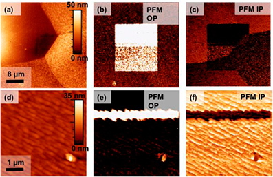
Figure 30. Polling measurements of BiFeO3 films across triple junctions ((a)–(c)) and grain boundaries ((d)–(f)). (a) PFM Topography, (b) out-of-plane, (c) in-plane, (d) PFM topography, (e) out-of-plane, and (f) in-plane. PFM contrasts were recorded after local application of a +12 V bias showing a 180° switching event. The images confirm the film gronw on ceramic has similar properties as those grown on single-crystals. Adapted from [221], with the permission of AIP Publishing.
Download figure:
Standard image High-resolution imageThese results demonstrate the potential of CSE in the design and growth of a wide range of complex functional oxides. They also open new directions for materials scientist and condensed matter physicists that could impact several areas. When CSE is coupled with scanning property measurements, high-throughput correlations can be generated between functional properties, film-substrate pairs, and crystal orientation, providing a library of physical property observations and expanding our understanding of engineering function into transition metal oxides. From the potential applications, it is further expected that this method could become a general rapid, convenient approach, for the search of metastable oxide films with a relatively low-cost fabrication, and this is probably one of the major topic to be explored. This will definitively speed the discovery of unexpected properties in oxide thin films.
Concluding remarks.
These examples demonstrated that structure-property relationships can be investigated for complex oxide heterostructures using the combinatorial substrate epitaxy approach, a high-throughput method for investigating the local epitaxy and properties of films deposited on polycrystalline substrates. Generally, efforts need to be intensified to rapidly prepare metastable phases in the form of thin films, and CSE is one of the potential approach to be used.
Acknowledgement.
Partial support of the Conseil Régional Basse-Normandie (Programe Asie) is acknowledged.
18. Topological oxide electronics
Masaki Uchida and Masashi Kawasaki
University of Tokyo
Status.
In the past, oxide materials have been complementarily used in conventional semiconductor technologies and devices. In particular, polycrystalline or amorphous oxide thin films with a large band gap have been widely adopted as gate insulators, capacitors, or transparent conductors. In recent decades, on the other hand, a number of unprecedented functionalities such as high temperature superconductivity, colossal magnetoresistance and electroresistance, and multiferroics have been discovered and attracted burgeoning attention for unique electronics applications as well as emerging new physics only realized in oxide materials. These properties and functionalities essentially originate from strong electron correlation in charge, spin, and orbital degrees of freedom. Technical advances in epitaxial film growth have opened the door to utilize the functional oxide thin films and also to explore atomically controlled oxide interfaces showing further emergent phenomena. Interface superconductivity and ferromagnetism are their examples demonstrating great potential of oxide heterostructures [224].
In the field of condensed matter physics, more recently, there is a growing awareness of other important degree of freedom, topology. Topology is the term used to describe or classify properties maintained for a continuous deformation in a given space. A topological state is thus intrinsically stable against perturbations favoring other different states, producing novel functionalities suited for storing and processing information as a state variable. Typical topological systems and their materials are summarized in figure 31. One example is a topological insulator, where the bulk bands have non-trivial topology in momentum space, giving rise to a symmetry protected conductive surface state [225]. This surface state is directly confirmed such as in bismuth selenides and bismuth tellurides, showing promise for dissipationless electronic devices. A more complicated state, connecting two sides of the surface state through the bulk, is also observed in transition-metal arsenides, called a topological semimetal. Quantum Hall systems represented by high-mobility GaAs heterostructure are another example of the topological phase, leading the research of edge states from the early period. The other example of topological systems is a magnetic skyrmion, where the spin textures have non-trivial topology in real space, giving rise to a topologically protected macroscopic spin object [226]. Typically, spins in two dimensions increasingly twist towards the center and show a vortex-like arrangement, as directly observed in chiral metals such as manganese silicides and germanides and a chiral insulator. The skyrmion behaves as a quasiparticle in a magnet, attracting rising attention as a stable information carrier.
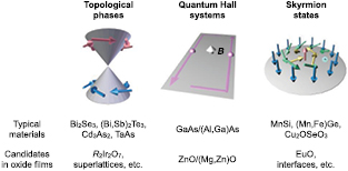
Figure 31. Typical topological materials and their candidates in oxide films.
Download figure:
Standard image High-resolution imageThe topological states are more generally characterized by topological numbers, which are respectively defined as integral of some spatial variances in the given space, and correspondent properties such as edge current or fictitious field robustly emerge in the unit of quantum conductance (e2/h) or flux (h/e). On the other hand, detailed performances of these topological properties, which are strongly dependent on fundamental parameters including electron correlation, spin–orbit interaction, and magnetic exchange interactions, as well as band gap and carrier concentration, require further improvement for their future applications. Oxide materials having the wide-ranging physical parameters are highly desirable for this purpose, and actually, several candidates in oxide films, interfaces, and superlattices are just beginning to be reported, as explained one by one in the following.
Current and future challenges.
Several perovskite and pyrochlore oxides with heavy elements such as iridium and bismuth or their superlattices have been theoretically suggested to exhibit novel topological insulator or semimetal phases, which originate from interplay of strong spin-orbit interaction and electron correlation [227]. For example, the discovery of a large gap topological insulator will lead to effective use of the dissipationless surface conduction at room temperature. As illustrated in figure 32, in addition, control of the topological phase domains and the correspondent dissipationless conductions is one of the significant goals for developing future low power consumption devices. Magnetic topological semimetals as expected in pyrochlore iridates R2Ir2O7, as well as magnetic topological insulators, are candidate systems for achieving magnetic control of the topological domains and conductions [228].

Figure 32. Concepts of topological electronics devices.
Download figure:
Standard image High-resolution imageRegarding quantum Hall systems, most efforts have focused on the even-denominator fractional quantum Hall state observed in the GaAs system. Its ground state has been extensively examined in the context of a non-abelian state, where quasiparticles obey non-abelian braiding statistics and their exchange operation is expected to be applied in topological quantum computation [229]. Clean oxide 2D electron systems can be alternative candidates for further advancing this research. In particular, ZnO/(Mg,Zn)O heterointerface, where the even-denominator state has been confirmed besides the GaAs heterostructure [230], is promising due to its higher controllablility of the ratio between Zeeman and Landau splitting energies. Determination of the non-abelian state, such as by demonstrating e/4 charge and full spin polarization, will pave the way for application to the quantum computation.
Magnetic skyrmions have much potential for application in future nonvolatile memory device, which has advantages such as high memory density and low driving current, compared to the magnetic bubble and racetrack memories [231]. While skyrmion crystals have been observed both in metals and insulators, the discovery in magnetic semiconductors is one of the important challenges for controlling skyrmion states through the carrier doping. Among many magnetic oxides, for example, ferromagnetic semiconductor EuO is one of the leading candidates, because topological Hall effect resulting from the fictitious magnetic field has been confirmed in its film form [232]. For creating small skyrmions for high memory density, it is necessary to modulate magnetic exchange interactions in materials, especially, the Dzyaloshinskii–Moriya interaction, which favors a cating of the two neighboring spins. Magnetic oxide heterostructures with tunable magnetic interactions at the interface are a highly promising system for realizing size-controlled skyrmion states, as atomic-scale skyrmions have been already demonstrated in metal heterostructures [233].
Advances in science and technology to meet challenges.
For directly confirming the topological surface state in candidate films or superlattices, in situ characterization integrating film growth and angle-resolved photoemission spectroscopy is remarkably helpful. Microscopy techniques for visualizing topological phase domains and/or the correspondent surface conductions are also needed to be developed for strongly promoting this research field. Regarding quantum Hall systems, advances in oxide molecular beam epitaxy technique will enable us to create new high-mobility 2D electron systems. Development of process techniques is also important for identifying the ground state such as by mesoscopic measurements. For demonstrating basic operations in skyrmion memory, an experiment combining transport measurement and direct observation using magnetic force microscopy or transmission electron microscopy is of key importance. Direct observation of interface skyrmion states is also technologically significant.
Concluding remarks.
Manipulation of topological properties in materials by external stimuli will trigger revolutionary changes in the present framework of electronics. The above described concepts are just a few examples that are expected to be realized in the typical topological systems—topological phases, quantum Hall systems, and skyrmion states. Once such basic operations of topological properties are demonstrated in oxide materials, it holds great promise for developing next generation innovative devices contributing low power consumption, quantum information, and magnetic memory technologies. The beginning of topological oxide electronics is envisaged on this frontier field.
19. Control of orbital reconstruction, metal-to-insulator transitions and topologically nontrivial phases at oxide interfaces
Rossitza Pentcheva
Theoretical Physics, Department of Physics and Center for Nanointegration Duisburg-Essen (CENIDE), University of Duisburg-Essen, Lotharstrasse 1, 47057 Duisburg, Germany
Status.
Technological demands driven by the fundamental limits of miniaturization of electronics devices call for the development of materials with tailored functionality that have the potential to substitute e.g. conventional semiconductors. Transition metal oxides (TMO) emerge as a promising class of such materials. Already in the bulk they exhibit a rich range of fascinating properties such as magnetism, superconductivity and ferroelectricity as a result of the interplay of charge, spin, orbital and lattice degrees of freedom [234]. Moreover, at their interfaces novel electronic phases can be stabilized that are not available in the parent compounds. This opens new avenues to design nanoscale materials with enhanced and new functionality. The past few years have witnessed an unprecedented activity in the field of oxide interfaces [186]. It is of paramount importance to achieve a fundamental understanding of the emergent physics at oxide interfaces. To this end, material-specific density functional calculations (DFT) can bring invaluable insight to identify and explore systematically the parameters that control this complex behaviour. In the following we will discuss the role of symmetry breaking, strain, exerted by the substrate, polar discontinuities, confinement, as well as variation in crystallographic orientation (see figure 33) in designing novel electronic ground states.
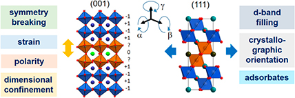
Figure 33. Side views of perovskite heterostructures along the (0 0 1) and (1 1 1) crystallographic directions along with parameters controlling the behaviour at oxide interfaces: symmetry breaking, strain, polar discontinuities, finite size effects. etc.
Download figure:
Standard image High-resolution imageCurrent and future challenges.
The ramifications of a polar discontinuity are evident in the case of the LaAlO3/SrTiO3 (0 0 1) interface. The AO/BO2 stacking in the perovskite structure ABO3 along the (0 0 1) direction leads to alternating positively and negatively charged layers in LaAlO3 (LAO) and formally neutral layers SrTiO3 (STO) and consequently an excess of 0.5 e at the TiO2/LaO interface (see figure 33). SrTiO3 quantum wells confined within LaAlO3 with symmetric n-type interfaces are experimentally more challenging to realize than the commonly investigated thin LaAlO3 films on SrTiO3 (0 0 1), but bear analogies to the recently investigated GdTiO3/SrTiO3 superlattices [177]. DFT + U results predict that in the thinnest quantum wells (N = 2) the electrostatic doping results in a charge and orbitally ordered state (alternating dxz, dyz at Ti3+) sites accompanied by strong octahedral tilts and rotations that are not observed in bulk STO (figure 34(a)) [235].
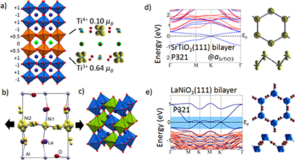
Figure 34. Mechanisms of electronic and orbital reconstruction at oxide interfaces obtained from DFT+U calculations: a) charge and orbital order at a polar (LaAlO3)4/SrTiO3)2(0 0 1) superlattice with a very narrow STO QW (N = 2) [235]; b) Band gap opening in (LaAlO3)1/LaNiO3)1(0 0 1) under tensile strain due to Ni-site disproportionation [238]. In contrast, a strong control of orbital reconstruction is possible in the double perovskite La2NiAlO6 c) which corresponds to a (LaAlO3)1/LaNiO3)1(1 1 1) superlattice [243]. A Dirac-point Fermi surface in d) (LaAlO3)4/SrTiO3)2(1 1 1) [245] and e) (LaAlO3)4/LaNiO3)2(1 1 1) [243] is unstable with respect to symmetry lowering that opens a gap.
Download figure:
Standard image High-resolution imageNovel effectively 2D behavior can be achieved even without a valence discontinuity. An example are heterostructures containing the paramagnetic metal LaNiO3 and the band insulator LaAlO3. Although the initially proposed control of orbital polarization by strain [236] could only partially be realized [237], intriguing electronic behavior was detected in this system: confinement of a single LaNiO3 layer leads to an opening of a gap under tensile strain (using e.g. SrTiO3 as a substrate) [238]. This metal-to-insulator transition (MIT) is driven by the interplay of quantum confinement, electronic correlations and strain and emerges from a disproportionation of Ni into two inequivalent sites with different magnetic moments but similar total charges (figure 34(b)) [238], similar to the mechanism identified in bulk nickelates [239, 240]. Upon increasing the thickness of the LaNiO3 layer the system quickly undergoes a dimensional crossover to a metallic state [241, 242]. In particular, the modification of bond angles and octahedral tilts under tensile strain effectively controls the bandwidth, triggering the MIT.
Advances in science and technology to meet challenges.
Currently, the interest is shifting from the much studied (0 0 1) oriented perovskite systems to the (1 1 1)-crystallographic orientation. In the [1 1 1] direction the stacking changes to AO3 and B layers (see figure 33), where each B layer forms a triangular lattice. In contrast to the (0 0 1) oriented superlattices, where the orbital polarization is limited due to the inherent covalency of the in-plane Ni–O bond, a strong control of orbital polarization can be achieved in (1 1 1)-oriented (LaNiO3)1/(LaAlO3)1 [243] or (NdNiO3)2/(LaAlO3)2 [244] superlattices. The spatial decoupling of the NiO6 octahedra either through layering (figure 34(c)) [243] or antiferromagnetic order [244] suppresses the covalency and enables orbital polarization. The strong influence of the crystallographic orientation coupled with the inherent high frustration in the (1 1 1)-oriented superlattices makes these systems very promising to host exotic electronic phases. Recently, the stabilization of a polar metallic state in NdNiO3 grown on LaAlO3(1 1 1) was reported, that is not accessible in the (0 0 1) orientation [245].
A new research area aims at designing topological states in oxide superlattices with (1 1 1) crystallographic orientation [246]. A bilayer in this configuration comprises a combination of two triangular lattices and forms a buckled honeycomb lattice which is known to host nontrivial behavior. This combined with the correlated, multi-orbital nature of transition metal ions leads the emergence of a Dirac-point Fermi surface in SrTiO3 and LaXO3 bilayers (X = Mn, Co, Ni) sandwiched between LaAlO3 as a spacer (see figures 34(d) and (e)). These states are interaction-driven (i.e. arise for a non-zero Hubbard U) and are protected by symmetry [243, 244, 247, 248]. Sublattice symmetry breaking of different origin leads to a Mott insulating gap. An interesting case emerges for LaMnO3 where a topological transition takes place from a Chern insulator with a sizeable band gap of ~150 meV to Jahn-Teller distorted trivial Mott insulator [248].
Concluding remarks.
The results achieved so far point to a series of parameters that can be used to tune the properties of oxide surfaces and interfaces in order to realize novel charge, magnetic and orbitally ordered states and enable control of functionality for applications in electronics and spintronics devices, as well as in energy conversion. Some major challenges for the future are the improvement in the theoretical description of strongly correlated systems e.g. by using hybrid functionals or dynamical mean-field theory, and, furthermore, the mastering of growth of highly polar surface orientations as the (1 1 1)-orientation, which has recently been demonstrated for nickelate superlatties (e.g. [244, 245]). Systems with this crystallographic orientation promise an even richer spectrum of possibilities concerning orbital reconstructions and topologically nontrivial states.
Acknowledgments.
Research supported by the German Science Foundation within SFB/TRR 80 'From electronic correlations to functionality'.
20. Kitaev exchange in hexagonal iridates and rhodates
Philipp Gegenwart
Experimentalphysik VI, Center for Electronic Correlations and Magnetism, Augsburg University, 86159 Augsburg, Germany
Status.
The honeycomb Kitaev model [249] describes a novel spin interaction which couples a spin with its three neighbors in a special way: each of the three different bonds realizes an Ising like coupling of one spin component, e.g. Sx, Sy, or Sz, respectively. Consequently along an 'x-bond' the x-components of the spins are coupled and respectively the two other bonds couple the two other spin components. This leads to a strong exchange frustration between the spins, as these cannot simultaneously align with all neighbours preferring distinct quantization axes. The exchange frustration prohibits even for ferromagnetic coupling a finite-temperature ordering and leads to a highly correlated, but strongly fluctuating low-temperature regime called quantum spin liquid (QSL). Kitaev's model requires a three-fold coordinated structure. It has attracted much attention, because it hosts a QSL with Majorana fermion excitations that could potentially be relevant for topological quantum computation [249]. An experimental realization is thus highly desired. However a bonding directional coupling of varying spin components in matter is generally quite unnatural and thus difficult to engineer.
In a seminal work, Jackeli and Khaliullin have predicted Kitaev exchange to arise in a certain class of 'spin–orbit' Mott insulating transition-metal (TM) oxides [250]. Figure 35(a), shows the d electron levels for heavy TM atoms in octahedral oxygen environment, as relevant e.g. for iridates with 5 electrons in the 5d shell. Here, the six t2g levels are split by spin-orbit coupling (which amounts to ~0.4 eV for iridates) in four Jeff = 3/2 and two Jeff = 1/2 states, the former being filled, the latter being half filled [251]. The resulting Jeff = 1/2 pseudospin has a wave function with orbital and spin contributions and one complex component. For the case of a 90° TM–O–TM bonding angle, as illustrated in figure 35(b), there appears a destructive interference between two different hopping processes. This leads to a bond-directional Ising type magnetic exchange (figure 35(c)) where only the Jeff = 1/2 components perpendicular to the plane formed by the two TM atoms and its O connections are coupled, like in a 'quantum compass' [251]. In Na2IrO3, edge-shared IrO6 octahedra are connected as displayed in figure 35(d), leading to a honeycomb configuration with three different bonds that couple x, y, and z-components of the Jeff = 1/2 pseudospins, respectively, as required for the Kitaev exchange.
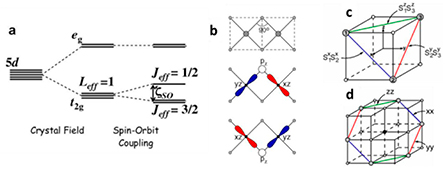
Figure 35. Kitaev magnetic exchange in spin-orbit Mott insulators. Splitting of 5d levels in an octahedral oxygen crystal electric field in the presence of strong spin-orbit coupling (a) Reprinted figure with permission from [250]. Copyright 2008 by the American Physical Society. Active bonds (in color) for edge-shared TM octahedra (b) Reprinted figure with permission from [251]. Copyright 2009 by the American Physical Society. Bond dependent Ising interactions in structural units with 90° TM–O–TM bonds (c). Design of the Kitaev model by combination of those units (d) Reprinted figure with permission from [251]. Copyright 2009 by the American Physical Society.
Download figure:
Standard image High-resolution imageCurrent and future challenges.
Na2IrO3 crystallizes in a layered C2/m structure with alternating stacks of Na-hexagonal layers and IrO6 honeycomb layers filled by another Na-atom [252]. Its electronic and magnetic properties indicate a Mott insulating state with a gap of order 0.35 eV and spin–orbit coupled Jeff = 1/2 moments. However, instead of displaying the desired Kitaev QSL ground state the material shows a zigzag antiferromagnetic ordering below TN = 15 K. While the observed spin–orbital entanglement of fluctuations above TN directly points to the dominance of the Kitaev interaction [253], small admixture of additional interactions, which are allowed by crystal structure symmetry in Na2IrO3, prevent the formation of the QSL. These are in particular next-neighbour Heisenberg and off-diagonal anisotropic exchange interactions as well as various further neighbour couplings [254]. The isoelectronic Li2IrO3 crystallizes in three different structures illustrated in figure 36. Honeycomb α-Li2IrO3 has so far only been synthesized in polycrystalline form [255]. Compared to Na2IrO3 it has compressed lattice parameters and a reduced gap ~0.16 eV. The Curie Weiss temperature of −33 K is significantly smaller than for Na2IrO3 (−116 K). An incommensurate magnetic ordering appears at 15 K whose exact structure is yet unknown. Isostructural honeycomb Li2RhO3 with Rh4+ is another most promising candidate material for Kitaev exchange [254]. Polycrystals did not show long-range ordering, but this needs to be confirmed on high-quality single crystals. α-RuCl3 is another honeycomb material with spin–orbit Jeff = 1/2 moments [256]. Advantageous compared to honeycomb iridates and rhodates, the RuCl6 octahedra in this material are likely closer to cubic symmetry because of only very weak van der Waals forces between the honeycomb layers. This is ideal for undisturbed Kitaev physics.
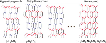
Figure 36. Various structures with three-fold configuration required for the Kitaev interaction that are derived from the planar honeycomb structure by out-of-plane rotations and their realization in various materials. Reprinted figure with permission from [257]. Copyright 2014 by the American Physical Society.
Download figure:
Standard image High-resolution imageAdvances in science and technology to meet challenges.
Crystal quality is a very important aspect for the characterization of candidate materials such as α-Li2IrO3 or isostructural Li2RhO3. Clean single crystals are required in order to determine the magnetic ground state and the dynamical properties related to the Kitaev interaction. Furthermore, it is promising to search for new materials with other than planar honeycomb structures. The three-fold coordination needed for Kitaev physics can also be realized in 3D structures. Figure 36 shows different synthesized variants of Li2IrO3 which realize 'hyper'- and 'stripy'-honeycomb configurations [257]. Unfortunately, β- and γ-Li2IrO3 both display long-range magnetic ordering at 38 K, though the configuration of the spins within the ground state could only be explained by a highly dominating Kitaev exchange. In order to achieve a Kitaev QSL, fine tuning of structural properties by chemical composition, hydrostatic or uniaxial pressure is required. Respectively for thin films epitaxial strain can be used.
In addition to the search for new candidate materials, it is promising to investigate signatures of Kitaev physics in dynamical properties. Recent Raman scattering on α-RuCl3 has shown a broad continuum below 100 K which cannot be explained by conventional two-magnon scattering and is compatible with theoretical expectations for fractionalized Majorana excitations in Kitaev materials [258]. Further dynamical investigations e.g. by inelastic neutron scattering, magnetic resonant x-ray scattering and ultrafast optical spectroscopy are following this direction.
Concluding remarks.
Driven by the discovery of topological insulators and motivated by the theoretical proposal of various novel states in correlated materials with large spin–orbit coupling, transition metal compounds with 4d and 5d elements such as Ru, Rh or Ir are currently the focus of strong interest. One field of intensive research concerns the search for solid state realizations of the Kitaev magnetic exchange. The latter induces strong dynamical frustration and supports a QSL with emergent Majonara fermion excitations that can be used for topological quantum computation. The required bond-directional exchange between differing spin components can be realized in three-fold coordinated structures of spin–orbit coupled moments. Several planar and 'hyper' honeycomb materials have been shown to realize Kitaev exchange. Structural fine tuning by chemical substitution, hydrostatic and uniaxial pressure or strain by choosing proper substrates for thin films can diminish additional exchange interactions which currently are spoiling pure Kitaev physics in real materials. Furthermore, the dynamical signature of Kitaev physics can be investigated in the paramagnetic state at elevated temperatures.
Acknowledgments.
Research supported by the German Science Foundation within SFB/TRR 80 and SPP1666.
21. A European action tracing the roadmap towards oxide electronics: perspective on nonvolatile oxide memories
Fabio Miletto Granozio1, Josep Fontcuberta2 and Nini Pryds3
1 CNR-SPIN UOS Napoli, Complesso Universitario di Monte Sant'Angelo, Via Cinthia 80126, Napoli, Italy
2 Institut de Ciència de Materials de Barcelona (ICMAB-CSIC), Campus UAB, Bellaterra 08193, Catalonia, Spain
3 Department of Energy Conversion and Storage, Technical University of Denmark, Risø Campus, Roskilde 4000, Denmark
Status.
The TO-BE COST action 'towards oxide-based electronics' (TO-BE)26, funded by the European Commission through the COST Association within the EU Framework Programme Horizon 2020, was started in 2014 and will run until 2018. The action gathers, at a European level, scientists from 29 European countries. TO-BE aims to create a strongly networked community of EU scientists active on synthesis, analysis, modelling and applications of transition metal oxides, with special emphasis on epitaxial heterostructures. TO-BE organises and funds semestral (spring and fall) meetings, biennial training schools and frequent international scientific missions between participating laboratories. The scientific activity is framed into three main work packages (WPs), as sketched in figure 37, named 'fundamental understanding', 'growth control' and 'towards application'. The last WP is focused on a wide range of applications as nanoelectronics, microactuation and microsensing, and energy conversion.
Figure 37. (a) Map showing the EU and associated countries currently participating to TO-BE COST action. (b) Schematic representation of the scientific activities.
Download figure:
Standard image High-resolution image
TO-BE main objectives include the publication by 2018 of an International Technology Roadmap for Transition Metal Oxides (ITR-TMOs). Our future roadmap aims to (i) trigger a 'paradigm shift' within the oxide-related research community, helping the scientists in the field to more effectively contextualize their research in the framework of the needs and trends of the mainstream semiconductor industry; (ii) identify oxide material and oxide-based devices that are really bound to play a role in the industrial development of novel technologies, (iii) increase awareness of the perspectives offered by oxide materials among the solid state community, the semiconductor industry, the general public and the policy makers. This section contributed to this roadmap is a first output of the activity that will eventually produce the future TO-BE roadmap.
Current and future challenges.
An overview of current and future challenges related to oxides is extensively provided by the other section published in this roadmap. To complete such an overview, it is mandatory in our opinion to include non-volatile memory technologies, a crucial topic in our action activity. We limit ourselves for brevity to emphasizing the role of oxides in so-called storage class memory devices. These are non-volatile memory (NVM) devices, i.e. memories that retain their information when power is switched off. They show promise to bridge the latency (time-access) gap presently open between fast volatile memories currently employed for code storage and execution (e.g. dynamic random access memories, DRAMs) and the slower non-volatile devices employed for data storage (traditionally magnetic hard disk drives and now, increasingly, flash NANDs). In the list below, following [261], a broad categorization of novel storage class memory devices is divided in two blocks: 'prototypical', for which the involvement of industry has already started, and 'emerging', for which research is still largely limited to the academic sector. Highlighted in bold in the lists below are the storage class memory types where oxides are expected to play a key role.
Prototypical non-volatile memory technologies are: (P1) FeRAM (ferroelectric-RAM); (P2) PCM (phase change materials); (P3) MRAM (magnetic-RAM) and (P4) STT-RAM (spin transfer torque-RAM).
Non-volatile memory technologies classified as emerging are: (E1) ReRAM (redox-RAM); (E2) ferroelectric memories (FeFET, ferroeletric field effect transistor and FTJ, ferroelectric tunnel junction); (E3) Mott memories; (E4) carbon memories and (E5) molecular memories. According to recent reviews from Marinella [259, 261], the performances of these devices are schematically reported and compared in table 1. Here, we restrict our revision only to Redox-RAM and ferroelectric memories, labelled as E1 and E2 in table 1.
Table 1. Synoptic table summarizing and evaluating different novel memory technologies, as reported in the ITRS-2013 ERD.
| Parameters | Prototypical | Emerging | |||||||
|---|---|---|---|---|---|---|---|---|---|
| P1 FeRAM | P2 STT-MRAM | P3 PCRAM | E1.1 Conducting bridge | E1.2 Bipolar filamentary | E1.3 Unipolar filamentary | E1.4 Bipolar interface effect | E2 Emerging FE memories | E3–E4–E5 Mott, carbon, molecular | |
| Scalability | + | ++ | +++ | +++ | +++ | +++ | +++ | ++ | ? |
| MLC | + | + | +++ | +++ | ++ | ++ | ++ | + | ? |
| 3D integration | + | ++ | +++ | ++ | +++ | +++ | +++ | + | ? |
| Fabrication cost | ++ | ++ | ++ | ++ | +++ | ++ | ++ | ++ | ? |
| Retention | ++ | ++ | ++ | ++ | +++ | ++ | + | ++ | ? |
| Latency | +++ | +++ | ++ | ++ | ++ | ++ | ++ | +++ | ? |
| Power | +++ | ++ | + | +++ | ++ | + | ++ | +++ | ? |
| Endurance | +++ | +++ | ++ | ++ | ++ | + | ++ | ++ | ? |
| Variability | +++ | + | ++ | ++ | + | + | +++ | ++ | ? |
Note: Freely rearranged from [261]. The number of plus marks is intended to quantify how successfully of the single device types have been meeting specific parameters.
Redox-RAMs (ReRAMs), presently considered as the most promising candidates for next-generation NVMs, are two-terminal passive device consisting of a nanometric thin oxide films, e.g. TaOx, TiO2, Al2O3, HfO2−x or SiOx, sandwiched between two metal electrodes. Under an applied electric field, a migration and redistribution of oxygen vacancies takes place [260], resulting in a large, measurable, reversible and non-volatile resistance switch between a high resistance state (HRS) and a low resistance state (LRS). Classified as emerging NVMs in 2013, ReRAMs are substantially shifting towards the prototypical class. ReRAM-based devices are commercially available27 today and are at the core of the 3D XPoint technology jointly released in 2015 by Micron and Intel28. ReRAMs are expected to be scalable below 10 nm and have been shown to possess large endurance, good retention and short latency (i.e. short access times). Their fabrication processes can be made CMOS compatible and allow for multilayering.
ReRAMs can be divided in different classes [261]. In table 1, the potential of (E1.1) electrochemical metallization bridge, (E1.2) bipolar filamentary, (E1.3) unipolar filamentary, and (E1.4) bipolar non-filamentary ReRAMs is assessed. Some present weaknesses of ReRAM technology are related to the undesirable initial forming steps, to the requirement of large switching currents, to the subsequent limitations due to crosstalk in high density cell arrays and (for bipolar devices) to the need for a bipolar power supply. The generation/creation of oxygen vacancies in thin films and their role in the filamentary process is an important issue which need to addressed and understood before these materials can be widely used in a device [262].
Ferroelectric tunnel junctions (FTJs), being the only family of ferroelectric memories to which we restrict here our interest, are rapidly progressing within the larger class of emerging ferroelectric (FE) memories. In FTJs a FE tunnelling layer is typically grown on a metallic oxide back-electrode and covered by a (different) top electrode. Large tunnelling electroresistance (TER) ratios between ON and OFF states, depending on the polarization direction of the FE barrier have been obtained [263]. Typical FE materials employed so far include BaTiO3, Pb(ZrxTi1−x)O3 (PZT), and BiFeO3. Once the use of ferroelectric doped HfO2 [264] will be demonstrated for application in FTJs, it would offer notable potential advantages. Being based on epitaxial heterostructures, FTJs are at the core of the TO-BE action. The tunneling conductance across the device is determined by the FE polarization direction and by the asymmetry in the screening length of the electrodes. This simple picture has guided the tremendous progress achieved in the last few years. TER values exceeding 104% (at room temperature) have been achieved in micron-size patterned devices and even larger values may be expected by performing modifications to the basic metal/FE/metal structure design. Such strategies include the introduction of slave layers behaving as Mott insulators [265] and the use of appropriate semiconducting electrodes [266] also allowing to modulate the effective barrier thickness [267]. From a more general perspective, additional control parameters of the memory state as light or strain can be exploited. In spite of its' potential, FTJ technology is as yet immature. Scalability below 50 nm, endurance, retention and sample-to-sample variability in patterned devices all need further investigations. Integration with present semiconductor technology is made possible by recent progresses on the growth of epitaxial complex functional oxides on Si [268]. While FTJ fabrication on Si platforms [269, 270] has been demonstrated, processing is not yet thoroughly CMOS-compatible and the full potential of integrating FTJ-on-Si has not been yet exploited [271].
Concluding remarks.
Beside extending the impressive trend of miniaturization, speed increase and unit cost reduction seen in last decades, oxide-based devices can be the key players within a revolutionary 'more-than-Moore' approach to non-volatile memories. A major example is given by memristors29 [272], presently considered as the key components of a future neuromorphic networks technology [273]. The first claim that a device based on resistive switching, based on a ReRAM-like device architecture, could be seen as the 'missing' memristor was reported in 2008 [274]. More recently other kinds of NVMs, including FTJs [275], have been proposed as an alternative to ReRAM for the fabrication of memristive devices. Non-volatile memories appear therefore to be one of the fields where oxide-based technologies may have a large impact, in next decade and beyond. This is an important challenge for oxide electronics that the TO-BE action aims to support in terms of research, networking and dissemination.
Acknowledgements.
This work has been partially supported by the TO-BE COST action MP1308. J F acknowledges financial support from the Spanish Ministry of Economy and Competitiveness, through the 'Severo Ochoa' Programme for Centres of Excellence in R&D (SEV-2015-0496) and MAT2014-56063-C2-1R, and from the Catalan Government (2014 SGR 734). F.M.G. acknowledges support from MIUR through the PRIN 2010 Project 'OXIDE'.
Footnotes
- 26
Further details about the MP1308 TO-BE COST action are found at the action web site http://to-be.spin.cnr.it/
- 27
See e.g. the Panasonic MN101L Resistive RAM based on a on a TaOx layer http://electronics360.globalspec.com/article/4246/embedded-reram-gets-into-distribution
- 28
- 29
Memristors are non-linear passive two-terminal electrical components first postulated on the base of their circuital properties principles, and regardless to their implementation, in 1971 by Leon Chua [272].