
Abstract
Amorphous zirconium oxide thin films deposited at room temperature, sandwiched between Pt and Ti electrodes, show resistive bipolar resistive switching with good overall performance figures (retention, ON/OFF ratio and durability). A variability observed during electrical characterisation is consistent with the coexistence of two different resistive switching mechanisms within the ZrO2 layer. Electron energy loss spectroscopy is used to map chemical variations across the device on the nanoscale. Partial oxidation of the Ti electrode creates an ohmic contact with zirconia and injects positively charged oxygen vacancies into the zirconia layer that are then responsible for resistive switching at the Pt / zirconia interface.
Export citation and abstract BibTeX RIS

Original content from this work may be used under the terms of the Creative Commons Attribution 3.0 licence. Any further distribution of this work must maintain attribution to the author(s) and the title of the work, journal citation and DOI.
1. Introduction
Resistive random-access memory (RRAM) has emerged as a candidate non-volatile memory technology that could transcend the physical and technical limitations of conventional RAM [1–5]. It relies on reproducible, history-dependent changes in the resistance of an 'active' material, but in most cases, the precise, mechanistic details of the resistive switching (RS) mechanism are unclear. In broad terms, there are two main mechanisms used to explain RS in binary metal oxides [1–9]. Filamentary RS occurs via the formation and dissolution of a localised, conductive filament that spans the active, generally oxide layer. Alternatively, interface RS occurs via wide-scale modification of the electrode/oxide interface. Several recent reports of device variability have highlighted deviations from these idealised mechanisms, for example, by suggesting their coexistence [8]. The impact of structural inhomogeneities, such as those introduced by defects in crystalline systems, is also under debate [10–16]. For example, grain boundaries in polycrystalline insulators are linked to higher on/off ratios and increased ease of switching because they act as fast migration paths. However, material granularity will limit scalability since devices of comparable size to the grains themselves will exhibit greater performance variability [13–15]. For this reason, fully amorphous switching layers may be better RRAM candidates because they offer structural homogeneity and do not require high temperature processing or the epitaxially-matched substrates that are needed for single crystal materials. Indeed, recent reports suggest that amorphous RRAM devices can offer an enhanced reproducibility and better long term stability in comparison to polycrystalline based devices [13–17]. Here, we report on amorphous ZrO2 based RRAM devices that were fully prepared at room temperature and demonstrate reliable RS and a resistance ratio greater than 100. Zirconia is a particularly good RRAM candidate because it has a high ionic conductivity [18] that may facilitate RS, has been extensively investigated as a substitute for silicon dioxide as a gate dielectric, and is compatible with conventional CMOS processes [19]. In contrast to our work, previous studies of zirconia-based devices have focused predominantly on (poly) crystalline zirconia, which is widely reported to support filamentary RS [19]. As in other RRAM studies that involve valence change mechanisms, the inclusion of an electrochemically active electrode that sources and sinks oxygen has also been discussed, with interfacial redox activity of titanium attracting the greatest attention [1, 20, 21]. Here, we focus on variability observed during electrical characterisation, and the clear coexistence of two independent RS modes with different switching characteristics. Analytical electron microscopy allows us to link this variability in RS to the presence of a partially oxidised Ti electrode under electrical cycling and possible crystallisation of the amorphous zirconia.
2. Methods
RRAM devices were prepared in a Pt/ZrO2/Ti/SiO2/Si(substrate) configuration. 170 nm of Ti was deposited as a bottom electrode onto thermally oxidised (300 nm thick oxide) Si substrates using pulsed laser deposition (PLD) of a clean Ti target within 0.5 mTorr of Argon. A KrF excimer (248 nm) laser was operated at 15 Hz and with approximately 2 mJ cm−2 energy density at the target surface. The amorphous ZrO2 switching layer, which is 38 nm thick, was then immediately deposited by PLD in 2 mTorr O2 without breaking the vacuum. An 80 nm thick platinum top contact was then deposited in a separate magnetron sputtering system, and conventional photolithographic techniques were used to pattern 400 μm2 devices. All depositions were done at room temperature, thereby retaining compatibility with a number of potential substrates and processing techniques, a particular advantage of amorphous RRAM devices. A cross-sectional transmission electron microscopy (TEM) specimen was prepared using standard techniques [22] on an FEI Company NovaNanolab focused ion beam (FIB) system. The usual plasma cleaning or annealing prior to TEM imaging was omitted in order to avoid accidental oxidation or crystallisation of the device layers. Scanning transmission electron microscopy (STEM) was performed using a probe corrected JEOL ARM200cF instrument operating at 80 kV, using a Gatan Quantum 965 spectrometer and 60 mm2 Bruker XFlash detector for electron energy loss spectroscopy (EELS) and energy dispersive x-ray spectroscopy (EDX), respectively. Electrical characterisation was performed under N2 on a temperature controlled stage, using a Keithley 2602 sourcemeter with a LabView interface. The platinum electrode was grounded for all measurements. For the forming and set processes, a current compliance (typically 2 mA) protected devices against hard breakdown of the initial high resistance state. No current compliance was used for the reset process. For pulsed measurements, a read voltage of 100 mV and write/erase voltage of 1.5 V was employed.
3. Results and discussion
Electron microscopy analysis of the cross-section of a typical device (after electrical switching) is summarised in figure 1. Figure 1(a) shows the cross-section in dark field STEM and indicates the layers to be smooth, continuous and structurally homogeneous. Electron diffraction (not shown) confirmed the ZrOx layer to be amorphous and there is little diffraction contrast evident in the STEM image. The spectrum imaging technique [23] was used to assess compositional variations within the two highlighted regions. Elemental profiles across the first region are presented in figure 1(b). Data were collected using EELS to map the Zr, O and Ti profiles and EDX to map the Pt. The integrated signals have been normalised in each case to aid comparisons. Our main interest is in the O profile across the active layer, since oxygen migration and variations in the oxidation state underpin both filamentary and interfacial switching mechanisms [1, 3, 8]. Figure 1(b) reveals an asymmetry in the ZrOx—electrode interfaces. At the Pt / ZrOx interface, the oxygen profile follows very closely that of zirconium, and the overlap of Pt and ZrOx signals at the interface is consistent with interfacial roughness. Platinum is electrochemically inert and there are no obvious reactions or variations in the oxide stoichiometry at the Pt / ZrOx interface. However, at the ZrO2 / Ti interface there is a clear extension of the oxygen signal beyond Zr and into the Ti layer, suggesting that a thin interfacial region of Ti has oxidised. Variations in the EELS fine structure, illustrated in figures 1(c)–(f) and collected from the second region of figure 1(a), confirm this oxidation. Figure 1(d) presents normalised Ti L23 EELS spectra obtained at the ZrO2 / Ti interface (full lines) and in the bulk of the titanium electrode (dashed lines), collected using the Dual EELS technique to allow the effects of plural scattering to be removed [24]. The spectra indicate a clear 1.0 eV chemical shift of the L3 and L2 main peaks, which is consistent with previous studies [25, 26] of oxidation and suggests specifically the formation of TiO. A lack of obvious crystal field splitting of the L2 and L3 features further suggests that the interfacial TiO is amorphous [27]. Higher resolution images (not shown here) did not reveal any evidence of crystallisation. Turning to the O K-edge, figure 1(f) compares the oxygen of bulk zirconia with that at the ZrO2 / Ti interface. The peak broadening of the bulk ZrO2 spectrum is consistent with the amorphous nature of the zirconia layer, whereas the spectrum obtained at the interface is in good agreement with previous results for amorphous TiO [28–30]. The changes in EELS fine structure are mapped in figures 1(c) and (e), allowing the width of the interfacial oxide to be estimated. Figure 1(c) shows that the chemical shift of the Ti L2,3 edge is restricted to a 3 nm thick region, thicker than the peak-to-peak roughness of as-deposited ZrO2, which was measured to be less than 0.5 nm by atomic force microscopy. Modification of the zirconia is similarly restricted: figure 1(e) shows that the Zr:O ratio is uniform until within 2 nm of the interface, where it drops by 10%. It is interesting that the change in zirconia stoichiometry illustrated in figure 1(e) is more spatially localised than the trends of figure 1(b), which were collected in a separate region, but only 50 nm away. The statistical relevance of this variation is unclear but does suggest slight chemical inhomogeneities within the active zirconia layer that cannot be observed in STEM imaging alone but which could have notable implications in electrical switching. Irrespective, the drop in ZrO2 oxygen content strongly suggests an interfacial reaction between ZrO2 and Ti to form TiO, which is interesting. The formation of TiO rather than TiO2 is notable because it suggests the formation of a quasi-ohmic interface since TiO is known to be electrically conductive. Indeed, our own measurements of symmetric Ti/ZrO2/Ti stacks show ohmic behaviour, in support of this assignment and in agreement with previous studies [1, 2, 20]. Together with reduction of the zirconia, the EELS data suggest the formation of an interface of the form ZrO2/ZrO/TiO/Ti. The implication of such an interfacial redox reaction is twofold: first, it suggests the creation of oxygen vacancies within the initially insulating zirconia layer, and second, it turns ZrO2/Pt into the active interface where RS occurs, which has not been described before for ZrO2 based devices [1, 20]. As the Pt is chemically inert, this then suggest a mechanism based on filamentary RS within the interfacial zirconia.
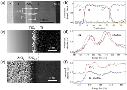
Figure 1. (a) STEM dark field image of the RRAM stack with the two regions used for EELS analysis indicated. (b) Normalised elemental distributions within region 1, derived from EELS (Zr, Ti, O) and EDX (Pt) analysis. (c) A map of the chemical shift of the Ti L23 edge within region 2, indicating a thin strip of oxidation at the Ti interface. (d) The Ti L23 EELS spectra used to construct the map in (c) and illustrating the chemical shift between bulk and interfacial Ti. (e) A map of the O:Zr ratio across the interface in region 2, indicating localised zirconia reduction. (f) A comparison between the oxygen K EELS edges collected from the zirconia film and from the Ti interface.
Download figure:
Standard image High-resolution imageInterestingly, the existence of oxygen vacancies is corroborated by the lack of an electroforming step: all devices exhibited RS without the application of a higher voltage pre-treatment. Characteristic current–voltage (I–V) sweeps of a typical device are summarised in figure 2. These were obtained after a small number of DC cycles. Figure 2(a) shows two bipolar switching modes, both of which were observed to occur within a single device. One trend would typically be observed for several voltage sweeps before changing, seemingly at random, to the second trend. Despite this variability, the devices showed good durability, withstanding >104 pulsed SET/RESET transitions. A 100-cycle subset of those transitions is presented in figure 2(b), which illustrates the device variability during SET/RESET pulsing of a typical device.
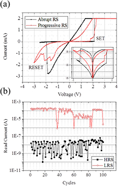
Figure 2. (a) I–V sweeps illustrating two distinct resistive switching behaviours. (b) Pulsed measurements which show discrete variability, consistent with two RS mechanisms.
Download figure:
Standard image High-resolution imageThe device switched reliably in every cycle, with good reproducibility of the insulating, high resistance state (HRS). The on/off ratio was typically 104 but would periodically dip to values around 103 and occasionally to as low as 101. We attribute this behaviour to the device switching between the two main modes of figure 2(a). Following the literature, we term the first mode (figure 2, black solid circles) 'abrupt RS', which exhibits ohmic behaviour in the low resistance state (LRS), abrupt SET/RESET transitions and a very favourable on/off ratio of 104. This contrasts with the second mode (figure 2, red open circles), which we term 'progressive RS' and which exhibits non-linear behaviour, progressive switching between states and an on/off ratio of 102–103. Both hysteresis modes have been described previously in the literature and have good on/off switching ratios that would be viable in a practicable memory element, however their coexistence in a single device is surprising and not so well documented. Interestingly, SET and RESET transitions were observed for positive and negative voltages, respectively, such that RS occurs as positive oxygen vacancies migrate towards (SET) and away (RESET) from the Pt/ZrO2 interface. Thus, if it is oxygen depletion that initiates the transition to a low resistance state, then the RS must occur at the Pt/ZrO2 interface. We infer that it is the localised electromigration of oxygen vacancies created at the Ti / ZrOx interface that ultimately gives rise to RS at the ZrO2/Pt interface. Conduction mechanisms can often be inferred from the slope of log(I)–log(V) curves [31–35], which are plotted in figures 3(a) and (b) for the set (positive voltage sweep) and reset (negative voltage sweep) operations, respectively. The LRS state of the abrupt mode is well described by a single, linear relationship, with unity gradient for both polarities, and indicates ohmic conduction throughout. It has previously been argued that an abrupt SET/RESET transition and an ohmic LRS is consistent with a metal-insulator transition [1, 3, 36–38], which would here occur in the ZrOx conducting filament, in the vicinity of the Pt / ZrO2. The trends observed here are consistent with other reports of Pt / ZrO2/Ti devices, which show that Ti electrodes enhance bipolar RS in ZrOx based devices [39–41]. However, these reports place the RS at the ZrO2 / Ti interface, which is not the case here. In the off state—i.e. when the device is not appreciably conductive—the trends of figure 3 are more consistent with space-charge-limited conduction [31, 33] and are therefore bulk limited, as expected for an insulator [33].
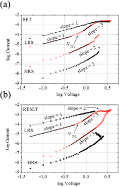
Figure 3. log(I)–log(V) plots used to assess the conduction mechanisms for the LRS and HRS during (a) SET and (b) RESET transitions.
Download figure:
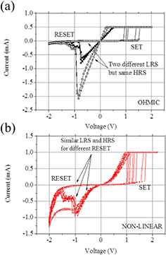
Standard image High-resolution imageConsiderable variability exists within this basic conduction mechanism for the abrupt RS mode and figure 4(a) illustrates five additional hysteresis loops recorded from the same device as that of figure 2. These loops were recorded during an automated sequence of DC voltage sweeps and were observed to be 'stable' for several cycles, before evolving. There did not appear to be any obvious degradation with time, and (as illustrated in figure 2(b)), the device would readily switch from a mode with low on/off ratio back to one with better performance; indeed, the hysteresis loops with low on/off ratios tended to be the least reproducible. All of the loops of figure 4(a) retain the abrupt RS characteristics seen in figure 2(a) with clear ohmic behaviour in the LRS. Typically, the RESET voltages and subsequent HRS characteristics hardly changed from sweep to sweep, whilst the SET transition was more variable. We propose that the variability in the LRS is due to the formation of conductive filaments with different geometries and therefore different resistances, but with similar activation energies given that the voltages at which switching happens are very similar. Turning to the progressive mode, a less abrupt SET followed by a progressive RESET transition suggests the formation of a conducting filament that does not completely connect the electrodes during switching, so that the current is limited by a thin layer of dielectric, or perhaps by the formation of a semiconducting filament [3]. The fits illustrated in figures 3(a) and (b) indicate that two different conduction mechanisms operate in the LRS [33–35]. Conduction is ohmic only at low voltages and the gradient in figure 3 departs from unity above ≈0.63 V (VTFL), changing to a trend that suggests the presence of trap-filled states (characterised by a gradient of 3 in the log-log plot of figure 3) [35, 39]. The HRS is again consistent with space-charge-limited conduction [33–35] expected for an insulator and is very reproducible from cycle to cycle. However, we again observe dynamic changes to the LRS, which would show good cycle-to-cycle reproducibility for some time, then change. Figure 4(b) illustrates a number of progressive RS hysteresis loops, all of which share the basic characteristics outlined above and which overlap remarkably well throughout the majority of the I–V cycle. However, there are notable differences in the SET and RESET characteristics. The SET process exhibits similar variability to that seen in figure 3(a) whilst the RESET process is in some cases a gradual variation (red open circles) and in other cases is mediated by more abrupt step-changes in conductivity (red filled circles). This variability in the non-linear behaviour could be explained by different trapping and de-trapping mechanisms taking place in slightly different regions of the Pt / ZrO2 interface, rather than at a single point. The existence of two types of RESET transitions in progressive mode indicates different reactions taking place at the ZrO2 / Pt interface.
Figure 4. I–V sweeps of variability within main switching behaviours (a) two discrete ohmic behaviours in 5 consecutive sweeps; (b) two discrete non-linear behaviours in 10 consecutive sweeps.
Download figure:
Standard image High-resolution image
It has been suggested that the existence of RESET transitions showing negative differential resistance (NDR) is explained by trapping/detrapping effects at a Schottky interface. Alternatively, the amount of electric current that passes through the RS oxide on the LRS will promote Joule heating that can also lead to crystallisation, and also give rise to NDR [30, 31]. Depending on the electrical current values, DC cycling RRAM devices can reach temperatures in excess of 900 K [11]. Ongoing crystallisation promotes changes and the formation of grain boundaries that could explain the existence of several conduction or fast diffusion paths with competing activation energies [15, 16, 26].
4. Conclusions
In summary, amorphous zirconia RRAM devices with very satisfactory overall properties, fully prepared at room temperature, were described. Transmission electron microscopy was used on a cross section so that EELS could be performed on all deposited layers that form the RRAM stack. The unambiguous oxidation of the titanium active electrode gives rise to an n-type conductive region that turns that interface ohmic, and simultaneously introduces oxygen vacancies that are vital for RS at the counter electrode. The switching characteristics are inherently variable, which we attribute to the existence of multiple switching mechanisms, including possible crystallisation of the amorphous layer. We propose that the coexistence of different RS modes is a characteristic of RRAM devices in general rather than a specific property of ZrOx. Notwithstanding the variability, our results suggest that low temperature deposition of amorphous ZrO2 films is a viable basis for RRAM devices.
Acknowledgments
This work was funded by the Engineering and Physical Sciences Research Council of the UK (EP/I00419X/1). Raw data relating to the study can be found at http://dx.doi.org/10.5525/gla.researchdata.258