
Abstract
Here we report a non-contact method for microwave surface impedance measurements of reduced graphene oxide samples using a high Q dielectric resonator perturbation technique, with the aim of studying the water content of graphene oxide flakes. Measurements are made before, during and after heating and cooling cycles. We have modelled plane wave propagation of microwaves perpendicular to the surface of graphene on quartz substrates, capacitively coupled to a dielectric resonator. Analytical solutions are derived for both changes in resonant frequency and microwave loss for a range of water layer thicknesses. In this way we have measured the presence of adsorbed water layers in reduced graphene oxide films. The water can be removed by low temperature annealing on both single and multilayer samples. The results indicate that water is intercalated between the layers in a multilayer sample, rather than only being adsorbed on the outer surfaces, and it can be released by applying a mild heating.
Export citation and abstract BibTeX RIS
1. Introduction
The transport properties of graphene have been an area of extensive study since the discovery of this exceptional material in 2004 [1–4]. The unique high mobility and massless Dirac particle behaviour for single-layer graphene at low frequencies and the quantum attenuation of graphene (πα attenuation per layer) at optical frequencies [5] have both spawned a number of investigations. On the other hand there has as yet been very little work reported on the microwave properties of graphene, more specifically on measuring the surface impedance of graphene. This is not surprising since it is in essence a rather low loss, high resistivity metal, transparent at optical frequencies. The complex permittivity at microwave frequencies may be expected to be similar, given the simple electronic structure of ideal graphene.
There are several methods to produce this atomically thin two-dimensional layer material [1, 6–8]. Amongst them, graphene oxide (GO) [6], a single layer of graphene covalently functionalized by oxygen atoms in the form of epoxy and hydroxyl groups, holds promise for a wide range of applications [9–12]. Graphene and graphene oxide have already been employed for several biosensing applications [13–15]. This latter material is particularly appealing because of its low preparation cost, due to water-based exfoliation of graphite oxide, its chemical versatility with regard to functionalization, and the easy assembly of individual flakes of GO into the form of thin films. Graphene oxide in its ideal form is an insulator. Thus it might be assumed that it would not be possible or useful to measure the microwave surface impedance of single-layer GO, given that the absorptive skin depth would be expected to be many orders of magnitude greater than a single atomic layer (0.35 nm). However, chemically reduced forms of GO (rGO) have shown much improved electrical conductivity compared with GO [11, 12]. Reduced GO is a thin film of conducting graphene platelets but is also expected to contain a variable amount of adsorbed or absorbed water, as well as other chemically bonded entities. It is also of interest because of its finite band gap, making it a potentially attractive material for transistor applications [12] and electrodes for supercapacitors [16]. Its outstanding mechanical properties and the ease of transfer to different substrates will enable other applications such as nanoelectromechanical systems (NEMS) [17, 18]. It has also attracted significant interest as a building block for novel applications in composites [9, 11]. Graphene-based actuators have shown that actuation depends on humidity and/or temperature [19]. Thus GO applications relying on interfacial properties may be important for applications. Nevertheless, to date little is known about the GO interfacial properties in different liquids.
The anticipated presence of water adsorbed or absorbed in samples of reduced GO arises from the method of preparation. Water is an exceptional liquid in many ways but its very high permittivity (both real and imaginary parts) at all frequencies up to the microwave region and beyond makes a microwave perturbation method particularly useful for studying the presence of small quantities of this liquid. Desorption of this water may produce a quantifiable effect on the surface impedance. No electrical contacts are required for this approach, removing one potential source of uncertainty.
2. Sample preparation and measurement technique
The samples used in this study were of GO synthesized by the modified Hummers method [6, 10, 12]. GO thin films were made by the vacuum filtration method as described by Mattevi et al [20], since this technique permits fine control of the GO thickness. The GO samples were transferred onto low loss single-crystal quartz substrates with size 10 mm × 10 mm. Various samples of graphene oxide and reduced graphene oxide have been prepared, including single-layer, five-layer GO and reduced GO on quartz, and then the samples have been installed in the sapphire puck system (see below) and measured. To confirm the layer number of these samples Raman measurements have been made and are discussed in section 4.
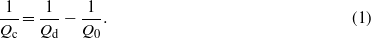
Our sapphire puck system contains a sapphire cylindrical resonator, 12.5 mm in diameter and 6 mm high which is mounted on a short quartz spacer in the middle of a copper housing (figure 1(a)), to reduce the associated microwave losses due to the Cu housing. Small microwave loop antennas protrude slightly into the base of the housing. The antennas' orientation and insertion may be adjusted to excite different modes of the sapphire resonator. The graphene/quartz sample is mounted on a Cu support and the distance between the graphene sample and the top surface of the sapphire puck can be adjusted. The typical separation between graphene and sapphire is 1.5 mm. A Hewlett Packard 8720 vector network analyser (VNA) is connected to the two antennas, allowing S-parameters to be measured at any frequency between 2 and 20 GHz. In addition, this instrument allows the centre frequency and 3 dB linewidth to be measured using internal software routines. A Labview virtual instrument program has been written which allows centre frequency, linewidth (and therefore Q value) and insertion loss of a single sapphire resonance to be monitored as a function of heated-stage temperature. The entire housing is mounted in a vacuum enclosure with a temperature sensor and heater (see figure 1(b)). The pressure is reduced to below 1 × 10⁻⁵ mbar to ensure good thermal isolation from external fluctuating temperature and to ensure that any adsorbates liberated on heating are effectively removed. This setup allows annealing of the resonator system at temperatures up to around 150 °C, an essential feature of the present experimental work.
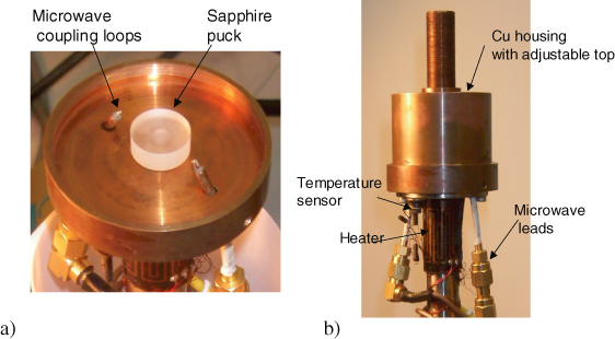
Figure 1. (a) The picture shows that the sapphire puck with quartz spacer is located in the middle of the bottom Cu housing. (b) Microwave cavity house with adjusting top and microwave probes are mounted on the top of the heated stage with a temperature sensor and heater.
Download figure:
Standard image3. Microwave surface impedance analysis
The technique described above enables quantitative measurement of the microwave surface impedance of thin film samples to be estimated, provided certain quantities are known. In the following two sections we summarize first a means for extracting the surface impedance (real and imaginary) from measured resonance data and in the second we show that, because of its high permittivity, even very thin layers of water can produce significant changes in surface impedance.
3.1. Relationship between Q values and surface resistance Rs
Upon suitable re-orientation of the coupling antennas at least four modes of the sapphire puck can be excited in the frequency range up to 20 GHz. These include the TM010 at 8.6 GHz and a series of TE01n modes with n running from 1 to 3 with frequencies 12.16, 14.34 and 17.89 GHz respectively. In view of the different radial field distributions of the TM and TE mode families, they sample any irregular property distribution of the graphene film differently. This provides a check that the perturbed frequency and linewidth values are representative of the whole of the surface of the graphene film rather than representing the response of a specific small section of it. Similarly the geometry factors for the n = 1–3 TE01n modes vary, although their end face mode distributions are identical. This can confirm the validity of the perturbation method to determine surface impedance [21, 22].
To calculate the geometry factor for the puck resonator we assume that we can analytically solve the field distribution arising for the eigenmodes of the puck. These eigenmodes are calculated in terms of dimensions, relative permittivity εr and a factor R which is the ratio of the electrical energy stored outside to that stored inside the sapphire puck. We follow the method described in the paper by Shen et al [23].
For a dielectric resonator which is closely coated with a conductor of surface resistance Rs and reactance Xs the following expressions hold, where the loaded Q is Q0 and the conductor Q is Qc and the dielectric Q is Qd and we ignore any radiation Qr. Then
If F is the fractional area of the end face which is covered by the graphene sample and R is the ratio of electromagnetic energy stored outside the resonator compared with the total energy including that stored in the dielectric:

where L is the height of the puck, λ is the free space wavelength of the microwave radiation and f0 and fd are the unperturbed and perturbed resonant frequencies respectively. Thus frequency and Q shifts arising from thin film samples allow Rs and Xs of those samples to be calculated, provided R and F are known. We will require a finite element model for the rather complex structure of the cavity plus substrate and we have not yet carried out the necessary modelling. In section 3.2 we show that a simple plane wave approach can give an indication of what effects we can expect from a thin layer of adsorbed water on a quartz substrate.
3.2. Surface impedance analysis
We consider plane wave propagation of microwaves perpendicular to the surface of the graphene coated quartz. There are several different materials involved, including the graphene layer, thin water layer, quartz and copper (see the schematic in figure 2) with various complex permittivities and thicknesses, but we are most interested in the influence of an adsorbed water layer. In the interests of simplicity we assume plane wave solutions since the sample is close to the sapphire puck resonator. Boundary conditions for the waves propagating in each direction are set out below.
At z = 0


At z = d1


At z = d1 + d2


where Zi and ki are the characteristic impedance and wave vector for the ith medium (see in figure 2).
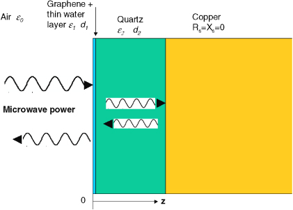
Figure 2. Schematic of multilayer of graphene with adsorbed water layer on top of quartz substrate with Cu backing. Here di and εi are the thickness and relative permittivity respectively of the ith region.
Download figure:
Standard imageThese six equations may be solved for the ratio of reflected wave E0− to the incident wave amplitude E0+. We assume the permittivities and thicknesses of the various dielectrics so all the k values and Z values are known, leaving only five unknowns. For water we assume that εw = 80 + i80 at microwave frequencies. Analytical solutions were obtained using Mathcad for a range of water layer thicknesses. The real and imaginary components for the ratio of absorbed to incident power relate to the fractional power loss and the fractional frequency shift respectively. These are summarized in figure 3. It is interesting that the reflected signal depends on the thickness of the quartz substrate as well as being linear in the water layer thickness for small thicknesses.
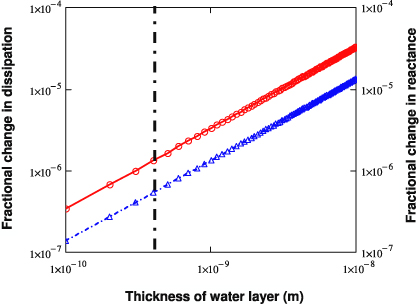
Figure 3. Schematic of the predicted contribution of a thin water layer to both loss (solid line with open circle) and reactive loading (dashed line with triangle) indicating the sensitivity of the method. A monolayer of adsorbed water has a typical thickness of 0.4 nm (see [24]) as shown by the dashed vertical line.
Download figure:
Standard imageIt is important to note that at present we have not managed to combine these two models for the influence of adsorbed water on the observed surface resistance and reactance of the composite sapphire puck and graphene sample. This will require a full finite element model extending over a very large range of scale, from 10 mm to 0.1 nm, stretching computing capability to its limits. We are working on this problem but note that the above models indicate the approach we will follow. In the meantime the high sensitivity of the resonant microwave method allows relative comparisons of different samples to be made and that is what we present in section 4.
4. Experimental results
We have carried out the measurement procedure described in section 2 on a number of reduced GO samples, including one with a single layer of graphene and a second with five layers, grown as described by Mattevi et al [20]. This growth technique is particularly useful as it permits fine control of the GO thickness. The GO samples were transferred onto low loss single-crystal quartz substrates with size 10 mm × 10 mm. Various samples of graphene oxide and reduced graphene oxide have been prepared, including single-layer, five-layer GO and reduced GO on quartz, and then the samples have been installed in the sapphire puck system and measured. (Note for GO samples where there are a large number of overlapping flakes we mean that the layer thickness is the average number of graphene layers perpendicular to the substrate surface, averaged over the entire substrate area.) Although there has been considerable evidence to support the correctness of the layer assignments it was thought advisable to carry out multi-point Raman spectrum measurements on each sample as reinforcing information. The Raman results are compared in the following figure 4. This shows that the five-layer reduced sample has a G peak which is approximately double that of the one-layer reduced sample. The G peak is an indicator of the amount of sp2 carbon that is being detected—it should rise for multilayer graphene systems, as is observed. The ratio of G peak to 2D peak intensities rises from 9 to 14 from one-layer to five-layer reduced samples. This ratio value is often used to infer the number of graphene layers observed to eliminate substrate effects [25]. Again, we see a rise in the value, in keeping with what is observed in multilayer graphene. Thus the Raman data confirm that the five-layer reduced sample is considerably thicker than the one-layer reduced sample.
The resonant frequencies and Q values were measured for several modes as a function of annealing cycles over a period of several weeks. In a typical heating cycle the system, under vacuum, was measured at a controlled temperature of 295 K then heated to more than 373 K and held there for a period. Then controlled cooling to 295 K was carried out and further microwave measurements recorded. This process was carried out a number of times for each reported sample.
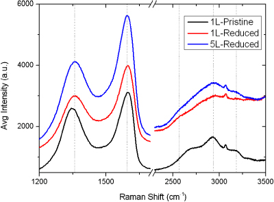
Figure 4. Raman spectra of three different graphene oxide samples. Each is an average over 12 separate spectra taken at 12 separate positions across the samples.
Download figure:
Standard imageIn the following four figures we compare the results obtained with a single reduced GO layer (figures 5(a) and (b)) and a five-layer reduced GO sample (figures 6(a) and (b)) as they are repeatedly annealed at temperatures around 100 °C (373 K). Although there is some considerable scatter (possibly due to more rapid heating and cooling on some runs) what is clear is that irreversible changes in both Q value and resonant frequency have been observed. The Q value and frequency change rapidly in early measurements, but after around 10 days the bulk of the changes in both values appear to have taken place. The change in microwave loss is approximately five times greater for the thicker sample (five layers) than for the single-layer sample. This leads to the conclusion that the adsorbed water is between GO layers, rather than being merely absorbed on the surface since in the latter case the change in surface impedance on annealing would be expected to be the same for both single- and five-layer samples.
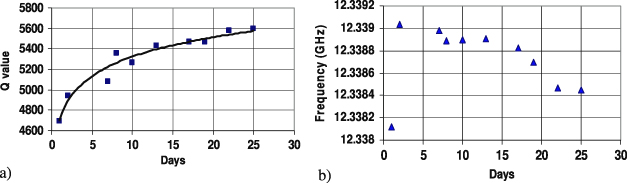
Figure 5. Results for single-layer reduced GO as a function of time and annealing cycles. The left-hand graph shows Q value and the right-hand graph shows frequency shift. The solid line in the left-hand figure provides a simple polynomial fit to the data but is mainly a guide to the eye.
Download figure:
Standard imageNote that the Q values achieved are still a factor of ∼4 × worse than for the empty sapphire puck resonator (∼2 × 10⁴). Future measurements will examine the limits to sensitivity of this non-contact method as a characterization and quality control technique. Higher quality quartz substrates with minimum dielectric loss should enable determination of high frequency transport properties of the reduced GO layers.
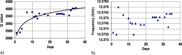
Figure 6. Results for five-layer reduced GO as a function of time and annealing cycles. The left-hand graph shows Q value and the right-hand graph shows frequency shift. The solid line in the left-hand figure provides a simple polynomial fit to the data but is mainly a guide to the eye.
Download figure:
Standard image5. Conclusions
Microwave surface impedance measurements have been little used previously for measurements of graphene samples. We show here that our measurement technique, combined with analytical modelling results, is sensitive enough to detect the removal of a monolayer of water and the results suggest that water is absorbed between reduced graphene oxide layers (i.e. intercalated) in multilayer samples. The results further show that the intercalated water in a multilayer sample can be released by applying a mild heating, which provides a simple first step towards optimization of reduced GO samples. The technique may also be applicable for characterizing other wafer scale graphene material prepared by chemical vapour deposition (CVD) or the SiC derived graphene method.
Acknowledgment
This work has been funded by the UK NMO EMT programme.