
Abstract
By depositing a graphene layer on the metallic film with subwavelength hole arrays, the tunable extraordinary transmission property based on the metal-dielectrics-graphene (MDG) structure has been investigated in the terahertz (THz) and near-infrared (NIR) regimes. The influences of operation frequency, composed materials, and the Fermi level of the graphene layer have been taken into account. The results show that by varying the Fermi level of the graphene layer, the transmission of the MDG structure can be tuned in a wide range and the modulation depth of the peak value of the transmission can reach more than 50%. But the tunable mechanisms in the THz and NIR regimes are quite different. In the infrared (THz) regime, the graphene behaves like the dielectric (metallic) layer; its dielectric constant decreases (increases) with the increase of Fermi level, resulting in the transmission increasing (decreasing). Compared with the metallic structure, the transmission of the semiconductor structure can also be modulated by using the doping or varying temperature; its peak position can also be changed in a much broader range. The results are very useful to understand the mechanism of the graphene plasmonic devices and to design novel filters, switchers, modulators, and sensors.
Export citation and abstract BibTeX RIS
1. Introduction
In 1998, Ebbesen et al discovered the enhanced extraordinary optical transmission (EOT) phenomenon, which means that when the optical light passes through subwavelength metallic hole arrays (MHA), the transmission shows an enhancement of several orders of magnitude with respect to the classical aperture theory [1]. Since then, much research work has been devoted to the EOT [2, 3], which has been investigated at different wavelengths [4, 5], hole shapes [6], and different lattice configurations [7]. This phenomenon is largely attributed to the resonant interaction of the incident light, with surface plasmons (SPs) generated by the subwavelength grating on the metal surface. SPs are electromagnetic waves that describe the collective excitations of electrons and propagate along the surface of conducting materials, with the properties of concentrating electromagnetic waves on the subwavelength scale [8–12]. The MHA structure manifests potential applications in many fields, such as near-field microscopy, resonators, and microlens [13, 14]. For instance, with the help of the semiconductor gain layer, the MHA structure can be used as resonators to fabricate SP lasers and has been realized experimentally [15].
Graphene, a flat monolayer of carbon atoms packed into a dense 2D honeycomb crystal lattice, has the merits of near-zero effective electron mass, high carrier motilities, and strong interaction with light in a broad frequency regime with the help of doping or regular structured patterns [16–19]. The conductivity of graphene can also be modified by means of chemical doping, electric field, or magnetic field [20, 21]. In addition, when the imaginary part of graphene conductivity is negative, graphene can support a transverse electric mode and display prospects for the development of optoelectronic devices [22, 23]. With those excited electronic transport properties, graphene is an alternative to traditional metallic materials [24, 25]. Recently, research based on graphene MHA or similar structures has been conducted [26–28]. For instance, the grapheme-coated metal films can be used as tunable molecular sensors in the near-infrared (NIR) region, and the SPs resonances can be enhanced because of the coupling between carriers in graphene and metal SPs [27]. Nguyen et al experimentally investigated the EOT phenomenon using pyrolytic graphite, which showed that though the conductivity of the graphite is smaller than that of the conventional metals, the graphite-based MHA structure manifests similar resonant transmission properties [28]. The graphene periodic micro- or nano-size antidot arrays have also been investigated to show that the GSPs are excited and exhibit strong absorption resonances [29].
To dynamically control the transmission of the MHA structure is a very interesting and important research topic, which can find many applications, such as in the design of switchers, filters, and phase shifters. Currently, there are some methods to modulate the transmission, but most of them depend on adjusting the structure parameters, using semiconductor-to-metal transition, or coating a dielectric layer on the MHA structure [30]. By depositing a graphene layer on the metal film with subwavelength hole arrays, we suggest the metal-dielectrics-graphene (MDG) structure can realize the modulation of transmission. Because the permittivity of the graphene layer can be changed by applying electric fields or chemical doping, the transmission of the MDG structure can be easily tuned. In addition, semiconductors can manifest 'metallic' characters, such as InSb in the THz regime [31, 32] or transparent conducting oxides and transition metal nitrides in the NIR spectral range [33]. Compared with the metals, the dielectric properties of the semiconductor can be modified by chemical doping or by varying the temperature, giving us much more freedom in the design of plasmonic devices. Therefore, the tunable transmission properties of the proposed MDG structure have been explored in the infrared and THz regimes, taking into account the effects of the Fermi level of the graphene layer, operation frequency, and the composed materials.
2. Theoretic model and research method
Figure 1(a) shows the sketch of the top view of the metallic subwavelength hole arrays. The lattice period lengths are dx and dy along the x and y directions, and the sizes of the holes are ax and ay along the x and y directions, respectively. The subwavelength metal hole arrays are covered first with a graphene monolayer patterned on the dielectric layer (SiO2), as shown in figure 1(b). The thicknesses of the metallic hole arrays, SiO2, and graphene layers are dMHA, dSiO2, and dg, respectively. The incident waves are normally transmitted through the MDG structure along the z direction.

Figure 1. (a) The top view of the schematic picture of metallic subwavelength hole arrays. The lattice period lengths are dx and dy along the x and y directions, and the sizes of the holes are ax and ay along the x and y directions, respectively. Figure 1(b) the side view of the schematic picture of metallic subwavelength hole arrays, which are deposited on the dielectrics layer (SiO2) and the graphene layer. The light is normally incident upon the metal film along the z direction.
Download figure:
Standard image High-resolution imageGraphene can be considered a 2D material and described by a surface conductivity σg, which is related to the radiation frequency ω, temperature T, phenomenological scattering rate Γ, and chemical potential (Fermi level, Ef). The conductivity of the monolayer graphene can be calculated by using the Kubo formula [34]:
where fd (ε) is the Fermi–Dirac distribution, j is the imaginary unit, ε is the energy of the incident wave, kB is Boltzmann's constant, and ℏ is the reduced Planck's constant. The first part of the equation is the intraband contribution, and the second part contributes to the interband contribution.
The dielectric constant of the graphene layer can be expressed as:

The permittivity of metal in the THz regime can be written as [35]:

where ωp and ωτ are the plasma and damping frequencies, respectively.
Besides metal, some large band-gap semiconductors (Al-doped ZnO (AZO), Ga-doped ZnO (GZO), indium-tin-oxide (ITO)), and transition metal nitrides (TiN, ZrN) can also be highly doped and exhibit metallic properties in the NIR regime. Furthermore, their losses are very small, and the real parts of the dielectric constant are comparable to that of the common dielectric materials, which are suitable for fabricating metamaterials devices. The frequency-dependent dielectric constants of metals and semiconductors in the visible and NIR spectral ranges can be described by using the Drude-Lorentz equation [33]:
in which m is the number of oscillators, fj is the oscillator strength, ωj is the resonant frequency of the oscillator, and γj is the oscillator damping frequency.
3. Results and discussion
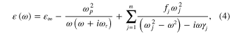
Figure 2 shows the transmission of the incident light through MDG structures at different Fermi levels in the NIR spectral range. The simulation results have been acquired by using the CST Microwave Studio, which is based on the finite integration technique. The frequency domain solver and unit cell boundary condition are adopted. The thicknesses of the Ag and SiO2 layers are 1200 nm and 5 nm, respectively. The Fermi levels of the graphene layer are 0.1, 0.2, 0.3, 0.4, and 0.5 eV, respectively. The lattice periodic lengths along the x and y directions (dx and dy) are both 1500 nm, and the hole lengths along the x and y directions (ax and ay) are both 600 nm. The EOT phenomenon, i.e., the resonant transmission efficiency higher than unity when normalized to the area, can be realized in the MDG structure. When a thin SiO2 layer is deposited on the metal film, the transmission decreases, and the peak position shifts to the longer wavelength. Compared with the conventional MHA structure, the transmission of the proposed MDG structure can be tuned in a wide range by adjusting the Fermi level of the graphene layer. Though the thickness of the graphene layer is very thin, only about 0.34 nm, its influence on the transmission is significant. Compared with the structure without the graphene layer (the peak value of the transmission is about 0.45), when the Fermi level of the graphene layer is 0.1 eV, the peak value of the transmission of the MDG structure decreases drastically, only about 0.12. This result from the graphene layer shows a large dielectric constant. As the Fermi level of the graphene layer increases, the transmission of the MDG structure increases significantly. The possible reasons are as follows. In the NIR regime, when the Fermi level is small, the real part of the dielectric constant of the graphene layer is positive; the graphene behaves much more like a dielectric layer. As the Fermi level increases, the absolute value of the permittivity of the graphene layer (|εm|) decreases, as shown in figure 2(b). When the Fermi level is 0.5 eV, |εm| shows a dip near 1.55 μm (193.5 THz). If the Fermi level of the graphene layer is beyond 0.5 eV, the sign of the real part of the graphene layer changes from positive to negative, and the graphene layer shows metallic properties. Therefore, the peak absolute transmittance can be tuned from 0.12 to 0.36 when the Fermi levels of the graphene layer change in the range of 0.1–0.5 eV. The modulation depth ((TEf0.5eV − TEf0.1eV)/TEf0.5eV) can reach more than 60%.
Figure 2. (a) The transmission of the MDG structure at different Fermi levels in the NIR regime. The thickness of the Ag film is 1200 nm. The lattice periodic lengths along the x and y directions (dx and dy) are both 1500 nm, and the hole lengths along the x and y directions (ax and ay) are both 600 nm. The substrate layer is SiO2 with a thickness of 5 nm. Figure 2(b) the dielectric constants of the graphene layer in the infrared regime. The Fermi levels of the graphene layer are 0.1, 0.2, 0.3, 0.4, and 0.5 eV, respectively. The insets in figures 2(a) and (b) show the top and back views of the unit cell of the MHA.
Download figure:
Standard image High-resolution imageHeavily doped semiconductors can also manifest 'metallic' properties and be considered alternatives to metals to fabricate SPs devices. Figure 3(b) shows the dielectric constants of several kinds of semiconductors and transition metal nitrides. Ag manifests the best metallic properties in the NIR regime. But the imaginary part of the dielectric constant of the doped semiconductor, such as AZO, is smaller than that of Ag, and its real part is also smaller. The transition metal nitride shows much better 'metallic' properties, but regretfully, the losses are also larger than that with Ag. The transmission of the incident light through ZrN-SiO2-graphene (ZrDG) structures at different Fermi levels is shown in figure 3(a). The ZrN layer is adopted as the 'metallic' film. The Fermi levels of the graphene layer are 0.1, 0.2, 0.3, 0.4, and 0.5 eV, respectively. The lattice periodic lengths along the x and y directions (dx and dy) are both 1500 nm, and the hole lengths along the x and y directions (ax and ay) are both 600 nm. The thicknesses of the ZrN and SiO2 layers are 800 nm and 5 nm. The EOT phenomenon is closely related to the dielectric constant of metal, and the large value of the ratio of the real to imaginary dielectric constants is beneficial to the SPs propagation. By adjusting the Fermi level of the graphene layer, the transmission of the ZrNDG structure can be modulated, as shown in figure 3(a). The transmission increases as the Fermi level of the graphene layer increases, which is similar to the results seen with the AgDG structure. When the Fermi level of the graphene layer is 0.5 eV, the absolute value of the dielectric constant of the graphene layer is small and shows a dip near 1.55 μm, leading to an increase in transmission. For the Fermi level of the graphene layer in the range of 0.1–0.5 eV, the peak value of the transmission of the ZrDG structure can be tuned in the range of 0.15–0.30, and the modulation depth ((TEf0.5eV − TEf0.1eV)/TEf0.5eV) can reach more than 50%. In addition, compared with the results seen with the AgDG structure, the transmission line width of the ZrDG structure becomes broader, which can be attributed to variation in the larger imaginary part of the dielectric constant and losses of the ZrN layer, as shown in figure 3(b).
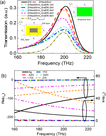
Figure 3. (a) The transmission of the ZrNDG structures at different Fermi levels in the NIR regime. The thickness of the semiconductor ZrN film is 800 nm. The lattice period lengths along the x and y directions are both 1500 nm, and the hole lengths along the x and y directions are both 600 nm. The Fermi levels of the graphene layer are 0.1, 0.2, 0.3, 0.4, and 0.5 eV, respectively. The insets in figure 3(a) show the top and back views of the unit cell of the MHA. Figure 3(b) the dielectric constants of several kinds of semiconductor layer in the NIR regime.
Download figure:
Standard image High-resolution imageFigure 4(a) shows the transmission of the MDG structures in the THz regime. Cu is adopted as the metal layer, with a thickness of 240 μm. The lattice period lengths along the x and y directions (dx and dy) are both 300 μm, and the hole lengths along the x and y directions (ax and ay) are both 120 μm. The substrate layer is SiO2 with a thickness of 0.3 μm. In the mid-IR and terahertz regimes, because the dielectric constant of metal is large, the transmission of light passing through the metal film is very small [36]. To enhance the transmission of the MDG structures, only part of the hole area is covered with the graphene layer. The insets in figure 4(a) show the top and back views of the unit cell of the MHA. In the THz regime, when the graphene is 'doped,' the graphene shows 'metallic' properties, with a negative real part of the dielectric constant and a positive imaginary part of the dielectric constant. Therefore, if a graphene layer is covered on the MDG structure, the transmission of the MDG structure decreases. Furthermore, the transmission of the MDG structure decreases with as the Fermi level of the graphene layer increases, which is rather different from the results in the NIR. The possible reasons are as follows. As the Fermi level increases, the negative real part of the dielectric constant of the graphene layer decreases and the positive imaginary part of the dielectric constant of the graphene layer increases, which means that at a larger Fermi level, the graphene layer shows a much better metallic property and larger losses. For instance, at the frequency of 1 THz, when the Fermi levels are 0.1, 0.2, and 0.5 eV, the dielectric constants of the graphene layer are −3.56 × 10⁵ + 2.20 × 10⁵i, −7.14 × 10⁵ + 4.39 × 10⁵i, and −1.78 × 10⁶ + 1.10 × 10⁶i, respectively. Therefore, the transmission of the MDG structure decreases as the Fermi level increases. Figure 4(a) shows that by varying the Fermi level in the range of 0.1–0.6 eV, the peak value of the transmission of the CuDG structure can be tuned in the range of 0.22–0.48, and the modulation depth ((TEf0.1eV − TEf0.5eV)/TEf0.1eV) can reach about 50%.
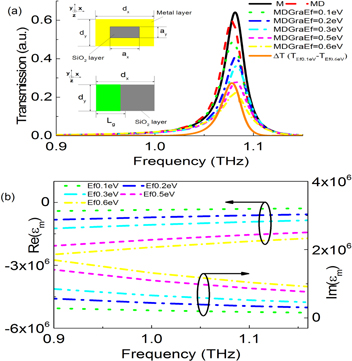
Figure 4. (a) The transmission of the MDG structures in the THz regime. The thickness of the metal film is 240 μm. The lattice period lengths along the x and y directions (dx and dy) are 300 μm, and the hole lengths along the x and y directions (ax and ay) are 120 μm. One-quarter of the hole area is covered with a graphene layer. The insets in figure 4(a) show the top and back views of the unit cell of the MHA. The substrate layer is SiO2 with a thickness of 0.3 μm. Figure 4(b) the dielectric constants of the graphene layer at different Fermi levels. The Fermi levels of the graphene layer are 0.1, 0.2, 0.3, 0.5, and 0.6 eV, respectively.
Download figure:
Standard image High-resolution imageSome semiconductors, e.g., InSb, also show metallic properties in the THz regime. Figure 5 shows the transmission of the InSbDG structures in the THz regime. InSb is adopted as the metal layer, with a thickness of 120 μm. The lattice period lengths along the x and y directions (dx and dy) are both 300 μm, and the hole lengths along the x and y directions (ax and ay) are both 120 μm. The dielectric layer is SiO2 with a thickness of 0.3 μm. The insets in figure 5 show the top and back views of the unit cell of the MHA; half of the hole area is covered with a graphene layer. As stated earlier, as the Fermi level of the graphene layer increases, the dielectric constant of the graphene layer increases, leading to a decrease in transmission of the InSbDG structure. Figure 5 shows that by varying the Fermi level of the graphene layer in the range of 0.1–0.6 eV, the peak value of the transmission of the InSbDG structure can be tuned in the range of 0.32–0.37, and the modulation depth can reach about 14%. It should be noted that the modulation depth of the InSbDG structure is not larger than that of the CuDG structure. Furthermore, the line width of the transmission of the InSbDG structure is much broader than that of the CuDG structure, which may result from the fact that the dielectric constant of the InSb is much smaller than that of the Cu. For example, at the frequency of 1 THz, the dielectric constants of Cu and InSb are −5.50 × 10⁵ + 1.20 × 10⁶i and −2.21 × 10² + 9.79 × 10²i, respectively.
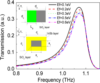
Figure 5. The transmission of the InSbDG structures in the THz regime. The thickness of the InSb film is 120 μm. The lattice periodic lengths along the x and y directions (dx and dy) are both 300 μm, and the hole lengths along the x and y directions (ax and ay) are both 120 μm. Half of the hole area is covered with a graphene layer. The insets in figure 5(a) show the top and back views of the unit cell of the MHA. The substrate layer is SiO2 with a thickness of 0.3 μm.
Download figure:
Standard image High-resolution imageFor the InSbDG structure, the temperature of the InSb layer also affects the transmission property. Figure 6 shows the transmission of the InSbDG structures at different temperatures. The thickness of the InSb layer is 120 μm. The insets in figure 6 show the top and back views of the unit cell of the MHA, and half of the hole area is covered with a graphene layer. The Fermi level of the graphene layer is 0.2 eV. The temperatures of the InSb layer are 280, 300, 350, 400, 500, and 600 K, respectively. As the temperature increases, the transmission of the InSbDG increases and the line width of the transmission decreases. The possible reasons are as follows. As the temperature increases, the carrier concentration of the InSb layer increases, showing much better 'metallic' properties. The larger negative real dielectric constant means smaller field penetration into the metal, and a smaller imaginary dielectric constant results in smaller losses. There is a tradeoff between the confinement and losses. The figure of merits (FOM) can be defined by Re(εm)2/Im(εm) [33]. As the temperature increases, the carrier concentration and plasma frequency of the InSb layer increases, resulting in the large negative real permittivity, which affects the FOM much stronger than the imaginary part of the dielectric constant. For instance, at the frequency of 1 THz, when the temperatures are 300, 400, and 500 K, the dielectric constants of the InSb layer are −41.95 + 126.77i, −172.30 + 407.93i, and −281.32 + 609.41i, respectively, and the values of the FOM are 13.88, 72.78, and 129.86, respectively. As a result, the transmission of InSb increases as the temperature increases. Figure 6 shows with the change in temperature, the peak value of the transmission of the InSbDG structure can be tuned in the range of 0.16–0.40 THz, and the modulation depth Tmod ((T600K − T280K)/T600K) can reach about 60%. The temperature also has a large influence on the peak position of transmission, which can be tuned in the range of 1.0–1.08 THz by changing the temperature. This probably results from the fact that the dielectric constant of InSb changes drastically as the temperature increases. This is very useful to fabricate plasmonic spectrometers, tunable filters, and beam steering devices.

Figure 6. The transmission of the InSbDG structures in the THz regime. The thickness of the InSb film is 120 μm. The lattice periodic lengths along the x and y directions (dx and dy) are both 300 μm, and the hole lengths along the x and y directions (ax and ay) are both 120 μm. Half of the hole area is covered with the graphene layer. The Fermi level of the graphene layer is 0.2 eV. The insets in figure 6 show the top and back views of the unit cell of the MHA. The substrate layer is SiO2 with a thickness of 0.3 μm. The temperatures of the InSb layer are 280, 300, 350, 400, 500, and 600 K, respectively.
Download figure:
Standard image High-resolution image
4. Conclusions
On the basis of the MDG structure, the tunable transmission properties have been given and discussed in the NIR and THz regimes, including the effects of the Fermi levels of the graphene layer, composed materials, and operation frequency. The results show that the transmission properties of the MDG structure can be widely modulated by adjusting the Fermi level of the graphene layer. The modulation depth of transmission can reach more than 50%, but the situations in the NIR and THz regimes are rather different. In the NIR spectral range, the graphene behaves like a dielectric layer, and the graphene permittivity decreases as the Fermi level increases, leading to the transmission increasing; while in the THz regime, the graphene layer shows metallic properties, and its permittivity increases in response to the chemical potential, resulting in the value of the transmission decreasing. In addition, some highly doped semiconductors can shows metallic properties. Compared with the metal structure, the transmission and modulation depth of the semiconductor structure are smaller. But the transmission of the semiconductor structure can also be modulated by varying the carrier concentration or temperature, and the peak position can also be changed in a wider range. These results are very useful to gain a better understanding of the mechanisms of the graphene plasmonic devices, which can find applications in the fields of polarization control, filtering, and switching.