

Abstract
Subwavelength plasmonic waveguides are the most promising candidates for developing planar photonic circuitry platforms. In this study a subwavelength metallic ridge waveguide is numerically and experimentally investigated. Differing from previous plasmonic waveguides, the metallic strip of the subwavelength ridge waveguide is placed on a thick metal film. It is found that the surface-plasmon-polariton (SPP) waveguide modes result from the coupling of the corner modes in the two ridge corners. The bottom metal film has a great influence on the SPP modes, and nearly all the evanescent fields of the SPP modes are tightly confined outside the ridge waveguide. Simulations show that 50% of the total power flow in the SPP mode can be confined outside the ridge waveguide with an area of only about λ2/20. The propagation length is still about 10 times the plasmon wavelength. Through comparison with a metallic strip placed directly on the dielectric substrate, the proposed ridge waveguide exhibits a much higher sensing performance. This plasmonic ridge waveguide with deep-subwavelength outside-field confinements is of significance in a range of nano-optics applications, especially in nanosensing.
Export citation and abstract BibTeX RIS
1. Introduction
The miniaturization of optical devices and circuits is important for integrated optics, but it is hampered by the diffraction effect of light. Surface plasmon polaritons (SPPs), the electromagnetic waves propagating along metal–dielectric interfaces, can be guided by metallic nanostructures beyond the diffraction limit [1, 2]. This remarkable capability has important applications in optical communications, computing, and sensing in high-integration circuits [1, 2]. In recent years, enormous attention has been focused on the design of various metallic structures to guide SPPs, including long-range SPPs (LRSPPs) guided by thin metal strips [3–6], channel plasmon polaritons (CPPs) guided by V-shaped metallic grooves [7–9], and dielectric-loaded SPPs (DLSPPs) guided by dielectric strips on the metal surface [10, 11] as well as the metal–isolator–metal (MIM) waveguide [12–14], slot waveguide [15, 16], wire waveguide [17–21], and hybrid plasmonic waveguide [5, 22, 23] modes. For most of these, the electromagnetic fields of the SPP modes are tightly confined in the plasmonic waveguides, such as in the dielectric layers or strips (LRSPPs [3–6], DLSPPs [10, 11], and hybrid SPPs [5, 22, 23]), substrates (wire waveguides [17, 19, 20] and slot waveguides [15, 16]), and the narrow metal gaps (CPP waveguides [7–9], MIM waveguides [12–14], and slot waveguides [15, 16]). Consequently, other media, particles, and molecules are difficult to immerse into the electromagnetic fields of the SPP modes, which considerably decreases the light–matter interaction in many applications, especially in optical sensing [24–26].
In this paper, a subwavelength metallic ridge waveguide is designed, and its modal properties together with the influence of the bottom metal film on the SPP modes are investigated numerically and experimentally. Numerical simulations show that the metallic ridge waveguide can support a symmetric SPP mode and an anti-symmetric SPP mode, which originate from the coupling of the corner modes guided by the two ridge corners. More importantly, nearly all (>99%) the evanescent fields of the SPP mode are tightly confined outside the metallic ridge waveguide because of the bottom metal film and the strong coupling of the two corner modes. As a result, the SPP modes supported by the metallic ridge waveguide have a long propagation length and a high sensitivity to the surrounding medium. It is found that the bottom metal film has a great influence on the SPP modes, such as the cut-off, mode shape, and propagation length. However, the dielectric substrate below the metal film has no influence on the SPP modes. Experimentally, the metallic ridge waveguide is fabricated on a gold film, and its propagation property is quantitatively measured by using back-side illumination [27].
2. Theoretical analysis
The proposed metallic ridge waveguide is depicted in figure 1, where a metallic strip with a width of w and a height of h is placed on a metal film with a thickness of t. This is quite different from previous designs in which the metallic strips or wires were directly placed on the dielectric substrates [3–5, 17–19, 28] or embedded in air [21]. Herein, the metallic strip and metal film are set to be gold. In the metallic ridge waveguide, there are two ridge corners, which can support the corner mode. The coupling of the two plasmonic corner modes can result in a symmetric SPP mode and an anti-symmetric SPP mode [4, 6], which are greatly influenced by the metal film. Because of the thick metal film, back illumination, which eliminates the noise of incident light, can be used in the experiment [27]. Moreover, this ridge waveguide with a small strip height can be easily fabricated.

Figure 1. Schematic and geometrical parameters of the ridge waveguide.
Download figure:
Standard image High-resolution imageFirst, the properties of the corner mode supported by the metallic corner in the ridge structure are numerically studied with the finite element method of Comsol Multiphysics. The metallic corner structure (w = ∞) is shown in the upper part of figure 2(a). The vacuum wavelength is λ = 830 nm and the permittivity of the gold is εAu = −26.61 + 1.665i [29]. When h is large enough (such as h = 1.2 μm, a typical value for experiments of CPPs [7–9] and wedge surface plasmons [8, 30, 31]), this metallic corner is similar to the metallic wedge structure of the angle α = 90° [8, 30, 31]. Simulations show that the metallic corner supports a plasmonic corner mode, the fields of which surround the corner, as shown by the lower part of figure 2(a). It is noted that the corner mode does not exhibit Gaussian distributions, and its shape varies with the structural parameters. Hence, it is difficult to define the mode area. To quantitatively describe the field confinements, the smallest area S, in which 50% of the total power flow in the SPP mode is confined, is introduced here. Based on this definition, the value of S is determined by


Figure 2. (a) Schematic of the metallic corner structure and field distributions (power flow for h = 400 nm). The arrows and the green line denote the vector of the electric field and a contour line of the power flows, respectively. (b) Effective refractive index, (c) propagation length, and (d) field confinements of the corner mode varying with the height of the metallic corner structure.
Download figure:
Standard image High-resolution imageIt is easy to obtain that the boundary of this area is a contour line of the power flows in the SPP mode, as depicted by the green line in the lower part of figure 2(a). Because of the ohmic loss, the effective index of the corner mode is a complex number (neff + i × nIeff). Usually, the propagation length is defined as L = 1/[2k0nIeff] [5, 8, 11, 19, 22, 28, 30, 31]. Here, k0 is the vacuum wave vector. The effective refractive index (neff), propagation length, and confinements of the corner mode in the metallic corner structure are calculated, and the results are shown in figures 2(b)–(d). From figure 2(b), it can be seen that the effective refractive index of the corner mode approaches that of the SPPs (n'eff = 1.0193) on the flat metal surface (violet dotted line in figure 2(b)) as h decreases. When the effective index of the corner mode is smaller than that of the SPPs on the flat metal surface, the SPP field cannot be confined in the x-axis direction, and thus the corner mode is cut off. Thus, the cut-off height of the corner mode is hcut-off = 100 nm. The propagation length and area (S) of the SPP mode supported by the metallic corner rapidly decrease with an increase in height, as shown in figures 2(c) and (d). At small heights, the long propagation length (figure 2(c)) is attributed to the poor field confinements (figure 2(d)), which is greatly affected by the bottom metal film. When h is large enough, the effective refractive index (neff), propagation length, and field confinements remain unchanged because the bottom metal film has little influence on the corner mode. These modal properties in figures 2(b)–(d) are very similar to that of the wedge surface plasmons [31].
As the ridge width of w becomes small, the corner modes supported by the two ridge corners will couple with each other. This can give rise to a symmetric mode and an anti-symmetric mode in the metallic ridge waveguide [4, 6, 32]. For the symmetric SPP mode in the ridge waveguide, the electric fields in the two corners are in-phase, as shown by the upper part in figure 3(a). For the anti-symmetric SPP mode in the ridge waveguide, the electric fields in the two corners are anti-phase, as shown by the lower part in figure 3(a). From figure 3(a), it can be seen that nearly all the evanescent fields of both the symmetric and anti-symmetric modes are tightly confined outside the ridge waveguide. To quantitatively investigate the modal properties of the ridge waveguide, the effective refractive index (neff), propagation length, and confinements of the SPP modes are also numerically calculated, and the results are displayed in figures 3(b)–(d). When the ridge width is small, the corner modes at the two corners strongly couple with each other. Consequently, the effective refractive index of the symmetric SPP mode is greater than that of the corner mode, while the effective refractive index of the anti-symmetric SPP mode is smaller than that of the corner mode [4, 6, 32]. Hence, the anti-symmetric SPP mode is not supported at the cut-off height (hcut-off = 100 nm) of the corner mode, as shown in figure 2(b). When the ridge width becomes large, the coupling between the corner modes at the two corners is very weak. Thus, the modal properties (including effective refractive index, propagation length, and confinement) of both the symmetric and anti-symmetric modes in the ridge waveguide are close to those of the corner mode in the metallic corner structure, as shown in figures 3(b)–(d). This strongly verifies that the symmetric and anti-symmetric modes originate from the coupling of the corner modes at the two ridge corners.

Figure 3. (a) Field distributions (power flow) of the symmetric SPP mode (top) and anti-symmetric mode (bottom) for h = 800 nm and w = 1000 nm. (b) Effective refractive index, (c) propagation length, and (d) field confinements varying with the width of the metallic ridge waveguide for different strip heights. (e) Field distributions of the symmetric SPP mode for different ridge widths when h = 300 nm.
Download figure:
Standard image High-resolution imageFor the symmetric SPP mode, its effective refractive index rapidly decreases with the increase of the ridge width and finally approaches that of the corner mode with the same height, as shown by the solid lines in figure 3(b). Its propagation length increases with the ridge width and also finally approaches that of the corner mode, as shown by the solid lines in figure 3(c). The propagation length is over ten times the SPP wavelength and thus is sufficient for a range of nano-optics applications [30, 33, 34]. For the anti-symmetric SPP mode, as the ridge width increases, its effective refractive index increases from that of the SPPs on the flat metal surface (violet dotted line in figure 2(b)) to that of the corner mode in the corner structure with the same height, as depicted by the dashed lines in figure 3(b). Thus, there is a cut-off width, which decreases with the increase of the ridge height, as shown in figure 3(b). The propagation length of the anti-symmetric SPP mode nearly remains unchanged, and it equals that of the corner mode (dashed lines in figure 3(c)) because of the weak coupling at large ridge widths.
For the field confinements, it can be seen that the symmetric mode can be tightly confined at small ridge widths (figure 3(d)) because of the strong coupling. However, the confinements of the anti-symmetric mode are poorer than those of the symmetric mode (figure 3(d)) due to the small neff of the anti-symmetric mode (figure 3(b)). To intuitively depict the field confinements of the symmetric mode, its field distributions are displayed in figure 3(e), where the fields become more and more localized when the ridge width decreases. This is quite different from the dielectric nanofiber [1, 26]. For example, for w = 50 nm in figure 3(e), 50% of the total power flow in the SPP mode is confined in the area of only about λ2/20 outside the ridge waveguide. This area is only about 5% of that in the corner mode (0.5λ2 × 2 for two corners in the ridge structures). However, the propagation length (LSPP = 7.4 μm) only decreases to 21% of that of the corner mode. The phenomenon of deep-subwavelength confinements in figure 3(e) can be utilized to realize nano-focusing [1, 35] and a nano-resonator [34] in a platform. When the sharp corners of the metallic ridge become rounded, simulations show that the propagation length of the SPP modes increases a little, and the cut-off width of the anti-symmetric SPP mode also increases.
Next, the properties of the metallic ridge waveguide at different wavelengths are investigated. As the metallic ridge width is fixed to be w = 300 nm, only the symmetric mode is supported based on the results in figure 3(b). The modal properties of the symmetric mode are calculated at different wavelengths, and the results are displayed in figures 4(a)–(d). It is observed that the effective refractive index decreases with the increase of the vacuum wavelengths, as shown in figure 4(a). At the same wavelength, the effective refractive index becomes large as the ridge height increases. At long wavelengths, the effective refractive index is close to that of the SPPs on a flat metal surface (violet dotted line in figure 4(a)). The propagation length of the symmetric SPP mode increases with the wavelength (figure 4(b)), which accords well with the confinements of the symmetric SPP mode, as depicted in figure 4(c). At λ = 1550 nm, the propagation length of the symmetric SPP mode is about LSPP = 240 μm, and 50% of the total power flow is confined in an area of about 1.9λ2 outside the ridge waveguide for w = h = 300 nm. This propagation length is greater than that of CPP waveguides [7–9], DLSPP waveguides [10, 11], the MIM waveguides [12–14], slot waveguides [15, 16], and wire waveguides [17–19]. It is noted that the propagation length of the SPP mode in the ridge waveguide is only a little smaller than that (LSPP = 290 μm) of the SPPs on the flat metal surface. Figure 4(d) presents the field distributions at four typical wavelengths. It is observed that the field confinement becomes poor when the wavelength increases. At long wavelengths, the field distribution approaches that of the SPPs on a flat metal surface, as shown by the bottom-right panel in figure 4(d). In any case, the evanescent field distributed outside the ridge waveguide can be easily manipulated to realize many applications, such as subwavelength sensors with an ultra-high sensitivity [36], ultra-small unidirectional SPP launchers [37, 38], polarization controllers, and manipulations of quantum-dot emission.

Figure 4. (a) Effective refractive index, (b) propagation length, and (c) field confinements of the symmetric SPP mode varying with the wavelengths for different strip heights. (d) Field distributions of the symmetric SPP mode at different wavelengths when h = 300 nm.
Download figure:
Standard image High-resolution image3. Experimental demonstration and discussion
Experimentally, the metallic ridge waveguide is fabricated and the propagation length of the guided SPP mode is quantitatively measured. By using the focused ion beam (FIB) technology, the metallic ridge waveguide is fabricated on a 450 nm thick gold film, which is evaporated on a glass substrate with a 30 nm thick titanium adhesion layer. Here, the subwavelength plasmonic waveguide is fabricated by etching two 2 μm wide grooves with a space of w on the gold film, leaving a subwavelength metal ridge on the metal surface to construct the plasmonic waveguide. SEM images of the metallic ridge waveguide in a sectional view and top view are displayed in figures 5(a), (b), respectively. Here, the smooth top surface of the metal strip and the rough surface of the bottom metal film are clearly observed. The measured parameters of the ridge structure are about w = 300 nm and h = 250 nm. Based on the above results, only the symmetric SPP mode is supported in the subwavelength ridge waveguide. Moreover, the glass substrate below the metal film has no influence on the SPP modes in the metallic ridge waveguide. This is quite different from previous plasmonic waveguides [3–5, 17–19, 28]. To excite the symmetric SPP mode with back-side illumination, a 200 nm wide rectangular aperture is fabricated on the metallic ridge waveguide, as depicted in figure 5(b). The back-illumination light first excites the aperture mode, which then excites the SPP mode along the ridge waveguide. To scatter the confined SPPs to free space for far-field detection, a 6 μm long decoupling grating (period of 800 nm) is fabricated on the right of the metallic ridge waveguide. The whole sample is depicted in figure 5(c). Herein, the separation between the aperture and the decoupling grating is L, and seven samples of different L are fabricated to measure the propagation length of the symmetric SPP mode guided by the metallic ridge waveguide.

Figure 5. SEM images of the metallic ridge waveguide in (a) sectional and (b) top views. (c) Typical experimental sample including an aperture and a decoupling grating.
Download figure:
Standard image High-resolution imageThe measurement set-up is shown in figure 6(a). A monochromatic light, which is filtered from a super-continuum light source (Fianium) by an acoustic optical tunable filter, is first polarized to be a p-polarized light. Then, the incident light is focused on the sample from the back by an objective (20×, NA 0.40), and the focused spot radius is about 100 μm. Here, the back-side illumination can eliminate the noise of the incident light [27]. The SPP mode is excited and then propagates along the metallic ridge waveguide until it is scattered by the decoupling grating. The scattered light is collected by a long working distance objective (100×, NA 0.50) and then imaged onto a charge-couple device (CCD). The CCD captured image at λ = 700 nm for L = 20 μm is displayed in figure 6(b), where a bright spot is observed on the decoupling grating. Moreover, it can be seen that the area of the bright spot is much smaller than that of the decoupling grating (the red dashed rectangle in figure 6(b)). Without the coupling plasmonic waveguide, the whole decoupling grating is lit up in the CCD pictures. Hence, the excited SPP mode propagates along the metallic ridge waveguide.

Figure 6. Measurement set-up and experimental results. (a) Schematic of the measurement set-up. (b) CCD picture captured at λ = 700 nm. (c) Relationship between ln(I) and L at λ = 700 nm in the experiment (black symbols). The red line is the linear fit line. (d) Experimental (red symbols) and simulation (black and blue line) results of the propagation lengths of the SPP mode at different wavelengths.
Download figure:
Standard image High-resolution imageIt is easy to obtain that the scattered intensity from the decoupling grating is

where, I0 is the SPP intensity at the aperture, and η is the scattering coefficient of the decoupling grating. To calculate the propagation length of Lspp, equation (2) is simplified to be [39–42]

Figure 6(c) displays the relationship between ln(I) and L at λ = 700 nm in the experiment, revealing a good linear relationship. From the slope of the curve in figure 6(c), the propagation length is calculated to be LSPP = 8.1 μm based on equation (3). This value is a little smaller than the simulation data (LSPP = 10.0 μm). The propagation lengths at long wavelengths are also measured in this way, and the results are depicted by the red symbols in figure 6(d), where the simulation results are denoted by the black line. It is observed that the propagation length becomes greater at longer wavelengths. It is also observed that the experimental results of the propagation lengths become much smaller than the simulation data at long wavelengths. This is mainly attributed to the fact that the fields of the SPP mode tend to be confined on the surface of the bottom metal film at long wavelengths (figure 4(d)). Thus, the rough surface of the bottom metal film (figures 5(a)–(b)) has a great influence on the propagation length at long wavelengths. The propagation length of the ridge waveguide with fabrication defects is calculated, and the simulation results (the blue line in the figure 6(d)) are in excellent agreement with the experimental data. This reveals that the surrounding medium (such as adherent particles and molecules) can also significantly affect the outside field of the SPP mode in the metallic ridge waveguide. This remarkable capability would greatly benefit waveguide-based sensors in highly integrated optics.
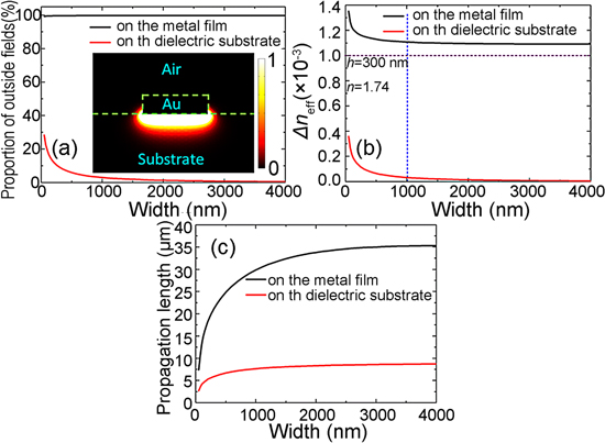
To test the validity of this benefit to the performance of waveguide-based sensors, the sensing performances of the metal strip placed on a metal film and a dielectric substrate [20, 43] are compared, and the results are shown in figure 7. For the metallic ridge waveguide, more than 99% of the evanescent fields of the SPP mode (figures 3(a),(e)) are tightly confined outside the metallic ridge waveguide, as depicted by the black line in figure 7(a). Thus, the variation of the effective refractive index of the SPP mode is large, and its value is greater than the refractive-index change of the surrounding medium (Δn = 0.001, violet dashed line), as shown by the black line in figure 7(b). While, for the metallic strip directly placed on the sapphire substrate (refractive index 1.74) [20], very small proportions of the total fields of the SPP mode (inset in figure 7(a)) are distributed in the air (outside the waveguide), as displayed by the red line in figure 7(a). It is observed that this small proportion approaches zero as the metallic strip width increases, and the vast majority of the fields of the SPP mode are distributed in the sapphire substrate (inset in figure 7(a)). Hence, the variation of the effective refractive index of the SPP mode is much smaller than the refractive-index change of the surrounding medium (Δn = 0.001), as depicted by the red line in figure 7(b). This indicates that the SPP mode guided by the metallic strip, which is directly placed on the sapphire substrate, is insensitive to the surrounding medium. For example, the variation of the effective refractive index in the ridge waveguide is about 35 times that in the metallic strip placed directly on the substrate for w = 1000 nm (blue dashed line in figure 7(b)). Moreover, the propagation length of the SPP mode guided by the ridge waveguide is much greater than that of the SPP mode guided by the metallic strip directly placed on the dielectric substrate (figure 7(c)) because of the large outside-field distributions. Therefore, the metallic ridge waveguide with large outside-field distributions possesses a pronounced feature in the sensing applications [24–26, 36].
Figure 7. (a) Proportions of the outside fields of the SPP modes guided by the metallic strip placed on the metal film (black line) and dielectric substrate (red line). The inset shows the typical field distribution of the SPP mode when the metallic strip (h = 300 nm and w = 1000 nm) is placed on the dielectric substrate. (b) Variations of the effective refractive index of the SPP modes guided by the metallic strip placed on the metal film (black line) and dielectric substrate (red line) when the refractive index of the surrounding medium is changed by Δn = 0.001. (c) Propagation length of the SPP modes guided by the metallic strip placed on the metal film (black line) and dielectric substrate (red line).
Download figure:
Standard image High-resolution image
4. Conclusion
In summary, the modal properties of a metallic ridge waveguide as well as the influence of metal film on the SPP modes were numerically and experimentally investigated. The SPP modes guided by the ridge waveguide resulted from the coupling of the corner modes at the two ridge corners. Due to the existence of the bottom metal film and the strong coupling, nearly all the evanescent fields of the SPP modes were tightly confined outside the ridge waveguide. For example, 50% of the total power flow in the SPP mode could be confined in the area of only about λ2/20 outside the ridge waveguide at λ = 830 nm when w = 50 nm and h = 300 nm. The bottom metal film had a great influence on the SPP modes, including the mode shape and propagation length. The propagation length ranged from 10 times the plasmon wavelength to nearly that of the SPPs on the flat metal surface, and thus it was sufficient for a range of nano-optics applications, especially in nano-lasers, nano-sensors, nano-resonators, and manipulations of quantum-dot emission. The subwavelength ridge waveguide was fabricated and its propagation lengths were measured in an experiment, the results of which accorded well with the simulation results. In comparison with a metallic strip placed directly on the dielectric substrate, the proposed ridge waveguide exhibited higher sensing performance. This plasmonic ridge waveguide with deep-subwavelength outside-field confinement might find important applications in plasmonic devices and circuits.
Acknowledgments
This work was supported by the National Basic Research Program of China (Grants 2013CB328704) and the National Natural Science Foundation of China (Grants 11204018, 61475005, and 11134001).