
Abstract
The electro-osmotic flow limit of detection and separation efficiency of glass channels machined using abrasive jet micromachining (AJM) were measured and compared with those for channels machined using conventional wet etching with hydrofluoric acid. It was found that the electro-osmotic mobility in AJM channels was similar to that in wet-etched channels, ∼4 × 10⁻⁴ cm2 V−1 s−1 for 20 µm channels, despite a two-decade difference in surface roughness. Similarly, limits of detection measured on the two types of chips were roughly comparable to each other and on the order of 1 nM (injected sample concentration). The separation efficiency calculated from TAMRA dye injections in AJM channels, however, was found to be significantly lower, ∼0.2–0.25 times, than that in wet-etched channels. The effect of surface roughness on the separation efficiency and electro-osmotic mobility in micro-channels is discussed in the context of the literature. Furthermore, experimental data concerning the effect of the AJM process conditions on the surface roughness are presented and discussed with the aim of exploring methods to improve surface quality in AJM. Commercially available self-adhesive elastomeric masks were found to be particularly suitable for rapid prototyping as they provided reasonably high resolution and machining flexibility.
Export citation and abstract BibTeX RIS
1. Introduction
In ∼20 years of concerted development of microfluidic devices, a variety of substrate materials have been used, but the vast majority of devices have been made using plastic or glass. Within these two material categories, the developer of a microfluidic analysis system must weigh not only the different chemical and physical properties of the materials, but also the different fabrication methods available for each. Regarding material properties, the developer might consider the UV transparency, higher thermal conductivity and chemical inertness of glass to be advantageous for one application, while for another, the mechanical ruggedness, flexibility and excellent visible spectrum transparency of a polymer might make it the preferred choice. In glass, the developer might weigh the direct-writing advantage and rougher etched surfaces of abrasive jet micromachining (AJM) against the more streamlined (but less flexible) nature and smoother surfaces of conventional photolithographic patterning and wet etching. Moreover, to what extent does reduced surface roughness confer a performance advantage to channels made by wet etching versus AJM? It is this question in the context of glass devices which is central to this study.
In AJM, the erosion caused by a high-speed (100–200 m s−1) stream of particles (10–50 µm) is used together with an erosion resistant mask to fabricate a pattern on a substrate [1–3]. The method has been used in a wide variety of applications such as the fabrication of steel micro-molds [4], micro-channels in PMMA [1, 2], and ball valve micro-pumps in glass [5]. AJM has several attractive features such as a high etch rate, machining flexibility, and low capital and operation costs. A more complete comparison between the achievable etch rate in AJM and conventional micro-fabrication processes, as well as other examples of AJM devices and apparatus can be found in previously published papers [1–3].
A potential disadvantage of AJM is the relatively high surface roughness that it imparts to the etched surface, several orders of magnitude higher than that resulting from conventional micro-fabrication methods. However, the effect of surface roughness on the functionality and performance of microfluidic devices machined using AJM is not well understood, and the literature concerning these effects is contradictory in some instances. For instance, Pu et al [6] found a negligible difference between the electro-osmotic flow (EOF) mobility in wet-etched (WE) and AJM channels, while Solignac et al [7] reported a 56% decrease in EOF mobility in AJM channels compared to WE channels (table 1). The deleterious effects of roughness on separation efficiency have been discussed by several authors [6, 8], but to our knowledge and surprise, the effect of roughness on optical detection sensitivity has not been considered.
Table 1. Summary of previous work comparing the electro-osmotic mobility of charged species and the separation efficiency in micro-fluidic channels fabricated using AJM and HF wet etching (WE).
| Channel size (µm) | Surface roughness Ra (µm) | µEO (cm2/(V ⋅ s)) | ||||||
|---|---|---|---|---|---|---|---|---|
| Source | Width | Depth | Nominal particle size used in AJM (µm) | AJM | WE | AJM | WE | Separation Efficiency |
| Solignac et al [7] | 100 | 30 | 30 | 8–10 | 0.030–0.060 | 3.4 × 10⁻⁴ | 7.8 × 10⁻⁴ | N/A |
| Pu et al [6] ('PBL' channel) | 109 | 50 | 9 | 1–5 | 0.003–0.015 | 7.08 × 10⁻⁴ | 7.64 × 10⁻⁴ | AJM 7–9 |
| times lower | ||||||||
| Pu et al [6] ('PBS' channel) | 92 | 22 | 9 | 1–5 | 0.003–0.015 | 7.34 × 10⁻⁴ | 7.64 × 10⁻⁴ | AJM 7–9 |
| times lower | ||||||||
| Belder et al [8] | 100 | 40 | 9 | 3–4 | 0.003–0.015 | N/A | N/A | N/A |
| Lacharme and Gijs [9] | 100–160 | 20–40 | 30 | 1 (After post- | N/A | 6.2 × 10⁻⁴ | N/A | N/A |
| heating) | ||||||||
| This study | 50 (AJM) | 20 | 10 | 0.4–0.6 | 0.002–0.005 | 4.2 ± 0.2 × 10⁻⁴ | 4.2 ± 0.1 × 10⁻⁴ | AJM 4–5 |
| 60 (WE) | times lower | |||||||
| This study | 330–350 | 100 (AJM) | 10 | 0.4–0.6 | 0.002–0.005 | 3.2 ± 0.1 × 10⁻⁴ | 2.8 ± 0.1 × 10⁻⁴ | AJM 4–5 |
| 150 (WE) | times lower | |||||||
Table 1 summarises results reported in the literature for the electro-osmotic mobility (not all using the same running buffer) and the separation efficiency of channels made using AJM compared with WE channels. Solignac [7] measured the velocity v of negatively charged 2 µm diameter fluorescent beads within microfluidic channels in the presence of a high field (2.5 kV cm−1). The channels that they produced using AJM were exceptionally rough, having Ra of 8–10 µm, which is as much as an order of magnitude rougher than those used in other studies as well as this study. They determined the electro-osmotic mobility (µEO) of the beads using equation (1) after a separate measurement of the electrophoretic mobility (µEP) in a relatively large beaker where the EOF due to the adjacent walls was negligible. In an electrophoretic separation, an ion's (or neutral's) electro-osmotic and electrophoretic mobilities comprise its total mobility µT, which together with the applied electric field E determine the ion's velocity v through
As shown in table 1, the electro-osmotic mobility of the charged beads in a 100 µm wide channel machined using AJM was less than half of the corresponding value for the channel machined using HF wet etching. This caused a reversal in the sign of the total mobility such that the negatively charged beads flowed to the anode in the AJM channel and to the cathode in the WE channel. Solignac et al [7] also observed that the channels produced using AJM caused a large broadening of the front of a plug flow of fluorescein isothiocyanate-labeled amino-acid mixture in 50 mM borate buffer (pH 9.2). These observations were attributed to the greater roughness of the powder blasted channels compared with those that were WE.
Pu et al [6] questioned Solignac's results, pointing to the very high roughness of their AJM channels and to the possibility of surface cracks remaining after the low-temperature bonding procedure that they used in the attachment of cover plates. Pu et al also found that the electro-osmotic mobility of powder blasted channels was similar to that of WE channels and that the separation efficiency of channels machined using AJM was 7–9 times lower than that of WE channels, but remained high enough to be suitable for most capillary electrophoresis applications. Lacharme and Gijs [9] also detected a lower separation efficiency in the channels machined in glass using AJM. Citing Pu et al's results, they attributed the reduction in separation efficiency to the relatively high surface roughness in AJM channels.
Belder et al [8] found that the separation efficiency of channels made using AJM was less than that of WE channels. They showed that coating the AJM channels with polyvinyl alcohol, and thereby reducing the surface roughness, increased the separation performance significantly, to a point where the resolution was comparable to that observed in an uncoated WE channel. They also noted that the separation efficiency was the same in channels with Ra values of 3 and 4 µm.
In this paper, EOF, limit of detection (LoD) and separation efficiency for both AJM and WE chips are investigated. The method developed by Huang et al [10] is used to calculate the electro-osmotic mobility in micro-channels via current measurements. The LoD and electrophoretic separation efficiency of chips made using AJM are also compared with those of WE chips. Finally, the effect of channel size on electro-osmotic mobility and LoD is discussed.
2. Experimental details
2.1. WE microfluidic chips
Micralyne Simple Cross Standard Chips (part PC-SC, Micralyne, Edmonton, Canada) were used for the WE chip experiments. These chips measured 16 mm × 95 mm × 1.1 mm and have 50 µm wide × 20 µm deep WE channels with 2 mm diameter cylindrical reservoirs at their termini (figure 1(a)). The long and short channels were 90.28 and 9.64 mm long, respectively, had quarter-turns next to each reservoir and their intersection bisected the short channel 9.39 mm along the long channel. The same channel layout was used for WE chips with deeper channels (300 µm wide × 150 µm deep).
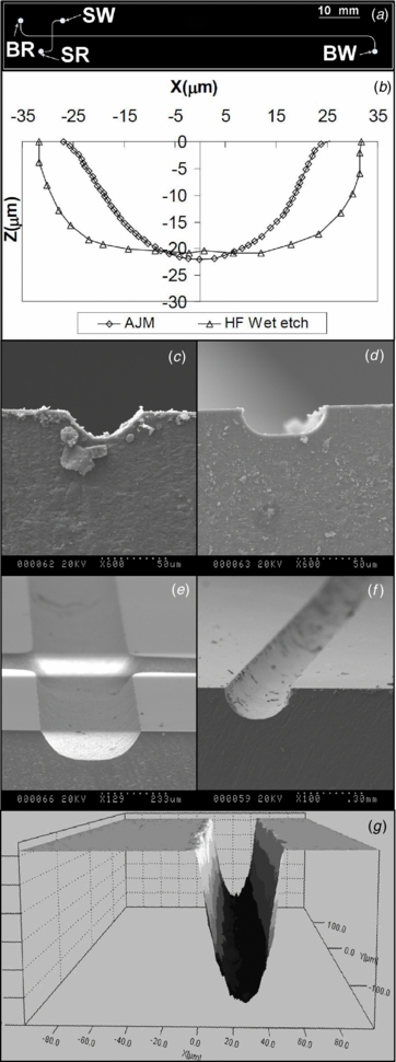
Figure 1. Channel layout, cross-sectional photos and scans. (a) Channel layout for both AJM and WE chips with reservoir designations per: SR = sample reservoir, SW = sample waste, BR = buffer reservoir, BW = buffer waste; (b) profilometer scans of both AJM and WE channels; (c–f) typical SEMs of the channels machined using AJM (c and e) or HF wet etching (d and f) for shallow channels (∼20 µm; b and c) or deep channels (∼150 µm; d and e); (g) 3-D image of AJM channel. Each unit in the Z-axis in (g) is 5 µm. Particulate matter seen in SEMs (c–f) reflects handling of diced sections in non-clean environments for imaging purposes.
Download figure:
Standard image2.2. AJM of microfluidic chips
Aluminum oxide particles of 10 µm mean diameter were blasted using multiple passes of a 0.3 mm × 3.8 mm rectangular nozzle. The particle mass flow rate was between 5 and 6 g min−1, the nozzle stand-off distance was 20 mm, and the nozzle was kept at 90° to the target surface [11]. Two types of microfluidic chips were machined: channels 50 µm wide × 20 µm deep and 300 µm wide × 100 µm deep, both machined into 1.1 mm thick Schott Borofloat™ glass (100 mm × 100 mm) in the pattern shown in figure 1(a), defined using an erosion-resistant polymeric mask [1–3]. The chips were cleaned using high pressure air and rinsed with water and acetone prior to the cross-sectional profile measurements.
The mask was manufactured using a photolithographic process by first printing the channel pattern on a clear acetate sheet using a high-resolution laser image setter (5080 dpi). This was then laid over a self-adhesive photomask material (RapidMask HD or RapidMask HT, IKONICS Imaging, Duluth, MN, USA) which was UV-cured using a 1 kW metal halide lamp (nuArc 26-1KS, The M&R Companies, NuArc, Glen Ellyn, IL, USA). Because it was relatively thin (50 µm), the RapidMask HD mask was well suited for transferring the small features of the 20–50 µm channel geometry. Its erosion resistance was adequate for the desired channel depth of 20 µm. The RapidMask HT mask (100 µm thick) was used for machining the deeper and wider AJM channels (300 µm wide and 100 µm deep). This set of larger channels was machined using AJM to compare with 300 µm × 150 µm conventional WE channels. Unfortunately, these larger AJM channels could not be machined to a depth of 150 µm because the self-adhesive mask (HT RapidMask) that was used eroded too quickly.
As seen in figure 1(a), the microfluidic channel pattern contained straight and curved channels, and relatively large diameter (2 mm) reservoir holes. Since the erosive efficacy distribution (i.e. a function of the product of the particle flux and velocity distributions) across the rectangular nozzle was non-uniform (as described elsewhere [12]), the effective width of the blast zone was not wide enough to machine the entire pattern to a uniform depth in a single pass. Therefore, a summation of multiple passes was used to obtain a uniform erosive efficacy to the surface using methods described previously [12].
The cross-sectional profile and roughness of the channels were measured using a WYKO white light interferometry profilometer. Scanning electron microscope (SEM) images of the features were obtained to examine the edge quality and uniformity of the channel.
2.3. Fusion bonding of glass cover plates
The AJM micro-channel borosilicate glass baseplates, described above, were fusion bonded at Micralyne using a process similar to that used for their standard microfluidic chips. The micromachined baseplate and cover plate with pre-drilled holes were first cleaned with soap, solvent and water rinses, aligned and bonded at approximately 700 °C for 1 h.
The elevated temperatures of the fusion bonding process reduced the surface roughness in the AJM channels by about 10% without deforming the channel structure in the 1.1 mm thick glass baseplate. As discussed below, the surface roughness in AJM channels was still two orders of magnitude greater than that produced by wet etching.
2.4. LoD, separation efficiency and EOF measurements
The performance of both the WE chips and those machined using AJM was tested using identical procedures. The EOF mobility was calculated for all AJM and WE channels, while the LoD and separation efficiency experiments were done with only 20 µm deep WE and AJM channels.
2.4.1. Reagents, solutions and instrumentation
For the LoD and separation efficiency experiments, both dye and buffer were required. A stock solution of 3.67 mM TAMRA fluorescent dye (Molecular Probes, Eugene, OR) in methanol was prepared. Dilute dye solutions of 367, 36.7 and 3.67 nM TAMRA in 1× TBE (Sigma; '1×' concentration of a tris, borate and ethylenediaminetetraacetic acid (EDTA) in aqueous solution: 89 mM tris(hydroxymethyl)aminomethane, 89 mM boric acid and 2 mM EDTA) were prepared via serial dilution. The running buffer was 1× TBE. Cleaning solutions of 1.55 M HNO3 and 1.01 M NaOH were prepared from concentrated nitric acid (69% HNO3, Anachemia), solid NaOH pellets (Fisher) and deionised water. For the EOF experiments, a dilution of 0.5× TBE was prepared and used together with the stock 1× concentration. The electrophoresis and fluorescence detection instrument used for all experiments was a Microfluidic Tool Kit (or µTK; Micralyne, Edmonton, AB, Canada) configured with the green laser-induced fluorescence (LIF) detection (λex = 532 nm, λem = 568.2 nm). Instrument software was used to capture current, voltage and LIF data at 25, 25 and 200 Hz, respectively; data were subsequently exported for further processing with Microsoft Excel. The µTK is described in detail elsewhere [13].
2.4.2. Chip preparation and storage
To prepare the chip at the start of each 4–8 h period of experimentation, cleaning fluids were drawn into the chip (WE or machined by AJM) by applying vacuum to one reservoir and supplying the other three with the appropriate fluid. For a given fluid rinse, a vacuum supplied by a 60 mL syringe was applied first to the buffer waste (BW) reservoir (figure 1(a)) for ∼10–15 min to slowly flush the chip. Daily chip preparation consisted of drawing through first HNO3, then NaOH, and finally the running buffer, 1× TBE. At the end of the period of experimentation, the chip channels had water drawn through them for 1–2 min and then were blown dry prior to storage of the chip under a dust cap.
2.4.3. LoD and separation efficiency experiments
After a chip was prepared, the BW, buffer reservoir (BR) and sample waste (SW) wells were filled with 3.5 µL of 1× TBE buffer, and the SR well was filled with 3.5 µL of the TAMRA dye solution at the concentration being evaluated. The chip was then inserted into the µTK instrument and the 2-step HV programme for pinched injection was executed. The two steps were (1) plug formation for 20 s, with SR, BR, SW and BW at 1.5, 1.1, 0 (ground) and 2 kV, respectively, and (2) separation for 60 s, with SR, BR, SW and BW at 5.1, 6, 5.1 and 0 kV (ground), respectively. (See figure 1(a) for reservoir designations.)
2.4.4. LoD data analysis
The unsmoothed electropherogram from each injected sample run was analyzed in Microsoft Excel to find the peak maximum, calculate the signal to noise ratio S/N and thereby determine the LoD (3σ) as follows. The peak height in the electropherogram signal S after the injection was defined as the difference between the peak maximum and the average baseline over the period from 6 to 3 s prior to the maximum value. The baseline noise N or σ was the standard deviation over the same 3 s segment. For each trace, the S/N value of the peak was calculated and the LoD was determined as the diluted sample concentration that would proportionally reduce the signal to a value of 3σ (S/N = 3). The process was automated through statistical functions to virtually remove human judgment; occasionally, noise spikes would mislead the peak maximum locator, and the range would be manually confined somewhat to omit the noise spike.
2.4.5. Separation efficiency data analysis
Using the peak and baseline values established in the LoD analysis, the up-slope and down-slope of the electrophoretic peak were determined by performing a linear regression on the data between 30% and 70% of the peak height on either side of the peak centre. The peak's half width W1/2 was calculated using these two lines, and the separation efficiency N was determined via
where tmig is the peak's migration time.
2.4.6. EOF experiments
Huang et al's method [10] was modified for use in a microfluidic chip similar to the measurements made by Crabtree et al [13]. Briefly, the SR, SW and BR reservoirs and the entire channel network were filled with 0.5× TBE buffer, and the BW reservoir was filled with 1× TBE. 4 µL was pipetted into each reservoir, but sufficient time was provided after the first well was filled with 0.5× TBE to ensure that the entire channel network was filled by the capillary action, as observed by eye (typically ∼30 s); this ensured that no air was trapped in the channels when the other reservoirs were filled. 6 kV (chips with 20 µm deep channels) or 1 kV (chips with 150 µm deep channels) was then applied to the BW, with the BR grounded and the SR and SW allowed to float. The current was measured by the µTK over the course of the run (200 s).
2.4.7. EOF data analysis
The current data from the BR reservoir were used to track the migration of the stronger buffer from the BW with the HV applied. The data were regressed along both linear portions and the intersection of both linear fits determined the migration time tmig required for the strong buffer to replace the weak one. Data intervals for regression were chosen to bracket the transition from down-slope to plateau; the down-slope interval was 5–25 s (chips with 20 µm deep channels) or 5–15 s (chips with 150 µm deep channels), while that for the plateau was 35–100 s. Given the channel length L = 90.28 mm, applied voltage V = 6000 V, and graphically determined tmig, one can easily calculate the electro-osmotic mobility µEO as

3. Results and discussion
3.1. Roughness and shape of AJM and WE channels
3.1.1. Roughness
A white light interferometry profilometer (WYKO, Bruker AXS Inc., Madison, WI) was used to measure the surface roughness of both AJM and WE channels. As expected, the AJM channels, with a surface roughness of ∼400–600 nm, were ∼2–3 orders of magnitude rougher than the WE channels at 1–5 nm. The effect of surface roughness on EOF, LoDs and separation efficiency is discussed in the following sections.
3.1.2. Shape
The cross-sectional profile of channels machined by AJM was generally different than that of WE channels (figure 1(b)). Low-aspect-ratio WE channels had a rotated 'D' shape at the edges and a flat portion in the middle (figures 1(d) and (f)). The transition from sidewalls to the middle of channel was not as pronounced in AJM channels. Low-aspect-ratio AJM channels had a shallow bowl shape cross-section with a smooth transition from the edges to the middle (figures 1(c) and (e)). For aspect ratios higher than 0.5, AJM and WE channels had approximately similar bowl-shaped cross-sections.
In contrast to WE channels, the AJM channels had a non-smooth edge, i.e. at z = 0 in figure 1(g). The edge quality in AJM depends on parameters such as the size of erosive particles and particle velocity (i.e. the impact energy). Ideally, smaller particles than the 10 µm alumina considered here should be used to machine channels as narrow as 50 µm. However, the resulting low impact energy makes them unattractive for machining purposes. An alternative option is to use small particles for final machining passes and smoothing. The mask thickness and quality, i.e. the maximum contrast that can be achieved between the cured and the uncured masking material, also affect the channel edge smoothness.
The 50 µm-wide channel intersection in the AJM channels was not as cleanly defined as in the WE channels. Figure 2 shows a comparison of the intersections of the two types of chips, with and without water in the channels. The difference was much less pronounced in the 350 µm wide channels. The channel depth and width at the intersection was influenced mainly by the mask quality. Although the HD RapidMask used for AJM machining provided good resolution for machining the 50 µm wide channel, it was vulnerable at the channel intersections, resulting in an increase in the channel width. The channel depth also increased as the channel widened, in keeping with previous work [12]. The HT RapidMask used for the 150 µm deep channels did indeed provide an adequate erosion resistance at the channel intersections; however, its resolution was too low for machining the 50 µm wide channel.
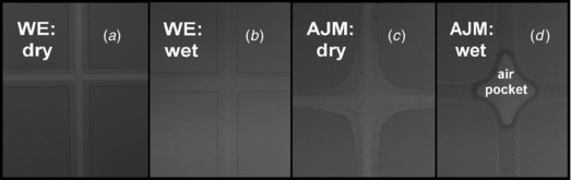
Figure 2. Channel intersections for WE and AJM chips. (a) Dry and (b) wet channel intersections for a WE chip and (c) dry and (d) wet channel intersections of an abrasive jet machined chip are shown. As described in the text, the serial nature of AJM means intersections are etched twice and are thus substantially larger and deeper than those in WE chips. The larger dimension both reduces capillarity, as suggested by the air pocket that appears during initial filling with solution (d) and leads to larger injected volumes given the same HV protocol. All optical micrograph images are brightfield at 200×; channel widths are ∼50 µm for both chips. Images (b)–(d) have given a +25 contrast enhancement in LView Pro software for clarity.
Download figure:
Standard image3.2. Limit of detection
Table 2 lists the average LoDs obtained at three different sample concentrations for both the WE and the AJM chips. In both cases, several data points were rejected due to either a poor peak shape with a pronounced tail, or an intermittent electronic interference that significantly increased the baseline noise.
Table 2. Average limit of detection (LoDAvg) values for n measurements in WE and AJM microfluidic chips with 20 µm deep channels.
| Chip type | (Sample) (nM) | LoDAvg ± 1σ (nM) | n |
|---|---|---|---|
| WE | 367 | 1.2 | 1 |
| AJM | 367 | 1.1 | 1 |
| WE | 36.7 | 2.0 ± 1.3 | 2 |
| AJM | 36.7 | 0.49 ± 0.05 | 4 |
| WE | 3.67 | 1.0 ± 0.2 | 2 |
| AJM | 3.67 | 0.41 ± 0.04 | 3 |
A preliminary hypothesis regarding a comparison of detection sensitivity for AJM and WE chips was simple and intuitive: microfluidic separations conducted in a channel created by abrasive jet machining, ∼2–3 orders of magnitude rougher than one made by wet etching, ought to show significantly poorer detection limits as a result of the optical scattering effect of the roughened AJM channel surface. The results of this study, however, suggested the contrary: AJM chip LoDs were 2–4 times better than those for WE chips at the lower sample concentrations.
The apparently better LoDs seen for AJM chips were likely an artefact of the method by which they were fabricated. WE chips have the entire channel network exposed to the HF-based etching solution, simultaneously, and the etch depth is controlled by limiting the time of the etch. As explained in section 3.1, the machining process used for 50 µm wide AJM channels generated channel intersections that were both quite broad, and also deep, ∼2× the channel depth elsewhere. The intersection of the AJM chip was much larger and deeper than that of the WE chip and had reduced capillarity which led to air pockets occasionally forming when the chip was first filled. The larger volume at the intersection of an AJM chip relative to a WE chip likely resulted in a larger sample plug being injected with the same HV protocol used to generate a pinched injection. Barring this artefact of AJM chips, the scattering generated by the considerably rougher surfaces in these chips seems not to have been a significant factor.
3.3. Separation efficiency
Graphical analysis depicted in figure 3 and described in section 2 was used to generate peak half-widths and separation efficiency data for all the injections at the three sample concentrations for both WE and AJM chips. These data are plotted in figure 4, together with the associated averages and standard deviations.

Figure 3. Example of electropherogram peak. Solid gray trace shows the PMT detector signal as the TAMRA zone passes through the LIF detection volume. Solid triangles and squares show the peak slope regressions from 30% to 70% peak height on the left-hand and right-hand sides of the peak. Horizontal trace shows the automatically calculated peak half-width (FWHM). Data were raw for the LoD analysis, but were smoothed for separation efficiency analysis, as explained in the text.
Download figure:
Standard image
Figure 4. Separation efficiency for WE and AJM chips. Efficiency calculated using peak half-widths in smoothed LoD data, plotted at each of the three sample concentrations (3.67, 36.7 and 367 nM TAMRA). Separation efficiency is between 4.0 and 4.9 times better for a chip made by WE versus AJM.
Download figure:
Standard imageData smoothing of the LoD electropherograms was required for the separation efficiency calculations. For the weaker concentration samples, 36.7 and 3.67 nM TAMRA, the noise fluctuation relative to the peak amplitude was significant (on the order of 30% for the 3.67 nM samples), which resulted in half-widths that were initially measured erroneously high along the peak profile (up to 3/4 peak height for the lowest sample concentration) which led to artificially short half-widths and thus higher peak efficiencies. For this reason, all of the traces were smoothed with a second-order 21-point Savitzky–Golay filter [14] using Igor Pro (v3.14, WaveMetrics, Lake Oswego, OR, USA).
The striking feature of figure 4 is the fourfold to fivefold worsening of separation efficiency for AJM chips. There may be several reasons for the inferior performance seen with abrasive jet machining, which are discussed in sections 3.5 and 3.6. First, the roughened surfaces themselves include undulations in the channel sidewalls which act to repeatedly expand and contract the analyte zone as it moves through the channel, promoting band broadening. Second, an approximately double injection volume and irregular channel intersection geometry present in the AJM chips lead to the injection of a longer plug which, though potentially advantageous for sensitivity, is a considerable source of band broadening as well.
3.4. Electro-osmotic flow
Current traces were acquired for both WE and AJM chips and were regressed along the two linear portions to find their intersection, as depicted in figure 5. The time at the intersection of the two lines was taken as the migration time for the stronger buffer to replace the weaker and was used to calculate the EOF mobility as described earlier.
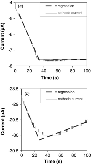
Figure 5. Current data used for EOF measurements. (a) Solid trace shows the actual current data acquired at the grounded electrode, while the 1× TBE buffer replaces the weaker 0.5× buffer in the 20 µm deep, 9.028 cm long channel of the WE chip. The dashed traces are the two linear regressions for the down-slope (regressed from 5–25 s) and plateau (regressed from 35–100 s), extended to intersect; their intersection at 33.6 s marks the migration time for the EOF calculation. (b) The same as for (a) but for the WE chip with 150 µm deep channels. Down-slope and plateau regressions (regressed from 5–15 and 35–100 s, respectively; see the text for discussion) intersect at 27.4 s.
Download figure:
Standard imageThe two linear regions were obvious for the 20 µm channel WE and AJM chips (figure 5(a)), while the 150 µm analogues showed the same trend, but curved upward and were less easily interpretable (figure 5(b)). Fixed data intervals were used for the linear segment regression to remove the possibility of analysis bias, but the fit was poor for the 150 µm channel chips nonetheless. The current profiles with these larger channels are thought to have been strongly perturbed by bulk solution backflow arising from both hydrostatic (siphoning) and Laplace pressures [13]. This backflow was generated from the significantly higher volumetric flow rate in the 150 µm channel chips which changed both the meniscus levels and shapes in both reservoirs. The resultant Laplace and hydrostatic back pressures would drive solution back toward the anode reservoir (with the higher strength buffer, from which the EOF originated) through the radial centre of the channel. Such a backflow would be comprised mainly of the weaker buffer from the cathode reservoir and would act to dilute the channel buffer concentration. This in turn would gradually decrease the current that the channel was carrying. As a result, the curve of figure 5(b) was pushed progressively upward with time as the growing volume displacement generated increasing pressures. We believe that this distortion of the current trace caused an erroneously small arrival time to be determined at the intersection of the two linear segments, which in turn generated an inflated value for the electro-osmotic mobility for these large channel chips. Estimating the effect of this replicate error could be achieved with fairly intricate finite-element analysis modelling, but was beyond the scope of this work.
The EOF data calculated from the current traces are shown in table 3 and display several trends. First, the EOF data for the 20 µm channel chips are fairly repeatable for both WE and AJM chip types, as shown by the relatively small standard deviations (RSDs of 2.9% and 3.8% for WE and AJM, respectively). Second, the EOF data are comparable for both chip types, as shown by the similar average values for each. Third, the EOF is observed to increase for the larger 150 µm channel chips though, as mentioned above, these values are suspected to have a negative bias from backflow. Fourth, our EOF values for either WE or AJM 20 µm channel chips are generally comparable to the values of others listed in table 1 (within a factor of 2); however, an explanation for the approximate twofold discrepancy is not obvious.
Table 3. Average EOF mobility (µEO) values for n measurements in WE and AJM microfluidic chips.
| Chip type | Channel depth (µm) | (µEO)Avg ± 1σ (cm2 (V s)−1) | n |
|---|---|---|---|
| WE | 20 | 4.2 ± 0.1 × 10⁻⁴ | 3 |
| AJM | 20 | 4.2 ± 0.2 × 10⁻⁴ | 3 |
| WE | 150 | 2.8 ± 0.2 × 10⁻³ | 2 |
| AJM | 100 | 3.2 ± 0.2 × 10⁻³ | 2 |
3.5. Surface roughness effects
The results showed that the surface roughness greatly affected the separation efficiency, but it had very little or no effect on the electro-osmotic mobility. Previous work [6–9] has attributed the lower separation efficiency to the higher surface roughness in AJM channels; however, little explanation has been provided. One hypothesis is that the electro-osmotic mobility and flow are reduced by surface roughness, thereby decreasing the separation efficiency to which it is linearly proportional [15]. Kirby and Hasselbrink [16] believe that the surface roughness influences the zeta potential and can affect the EOF; however, they viewed these effects as being negligible for conventional WE micro-channels.
In contrast to the presented observations (table 3), the numerical work of Hu et al [17, 18] suggested that the EOF pattern and mobility are greatly affected by roughness, mainly due to its effect on the flow pattern in the channel. This explanation is in contrast with what has been observed in this study, and also in previous work [6, 9]. One hypothesis that is consistent with the results of this study is the enhanced mixing, and consequently reduced separation in excessively rough channels [19].
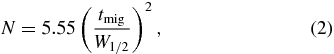
A factor affecting separation efficiency is the fluctuation of capillary radius. Studies have shown that the effect of the flatness of capillary walls on electrophoretic resolution is very significant. The time–width increase of eluted zones shows a sixth-power dependence on fluctuations in capillary radius [15]. For conventional WE channels, this effect is insignificant as the reported average roughness of less than 1 nm on a nominal capillary diameter of 20–100 µm would lead to a dispersion increase of 0.04% at the most [15]. However, the situation is different for AJM channels. The mathematical formulation for the plate number sheds some light on this dependence. The plate number (the measurement denoting the separation efficiency) is inversely proportional to the diffusion coefficient D:
and

where C is a constant, Pe is the Peclet number (Pe = Re ⋅ Sc, where Re and Sc are the Reynolds and Schmidt numbers). Variations [15] in the channel width change Pe and consequently D and the plate number N.
3.6. Effect of channel profile shape
As shown in figure 1 and discussed in section 3.1, the cross-sectional profile of the channel machined using AJM was slightly different from that of the WE channel. The effect of the channel shape on the separation efficiency is not well understood, but it likely results in a change in the flow pattern and factors such as Reynolds number and Peclet number. The effect of channel shape on pressure-driven flow in micro-channels was modeled by Dutta et al [20] who investigated channels of varying shape. They found that the mechanism by which the separation efficiency is disturbed by the channel geometry is related to the effect of channel geometry on fluid shear. The fluid shear degrades the separation resolution by dispersing the solute slugs as they travel through the micro-channels. Dispersion is increased by the higher drag on the fluid near the rough channel walls. Modelling and calculating the dispersion coefficients for the different geometries shown in figure 1 were beyond the scope of this work. It is however believed that the reduced separation efficiency is collectively due to the differences in both channel shape and roughness as described in the previous section.
4. Conclusions
Electro-osmotic mobility, LoD and separation efficiency of microfluidic channels machined using both AJM and wet etching were studied and compared. Electro-osmotic mobility and LoD were nearly identical for both AJM and WE chips, while separation efficiency was, as expected, significantly degraded in AJM chips due to their greater roughness.
The surface roughness was found to have a negligible effect on the electro-osmotic mobility. It is believed that the surface roughness distorts the electric field near the liquid–solid interface in electrophoresis. This distortion results in a non-uniform electro-osmotic velocity and, hence, a non-uniform electro-osmotic mobility distribution within the channel cross-section. Our results and those of others support the hypothesis that (a) the disturbance is negligible and does not affect the mobility of charged species in the charged field, and/or (b) the disturbance is limited to a narrow region, i.e. the mobility is still fairly uniform within the channel and only disturbed close to the channel surface.
Limits of detection were somewhat better for AJM chips versus WE chips; this small difference was attributed to differences in the channel intersection where the sample plug was formed. It was somewhat surprising that the increased roughness in the AJM chips was not more detrimental to the LODs attained in these devices, though we have not found similar studies in the literature for comparision.
The separation efficiency was dramatically reduced in the channels machined using AJM compared with wet etching. The reduction in separation efficiency was attributed to the increase in the dispersion coefficient, which is a function of the Peclet number, which itself depends on the Reynolds number. Specifically, the irregularities in the surface of the channel machined using AJM increased the Reynolds number and, consequently, the Peclet number, resulting in a higher dispersion coefficient, i.e. a higher effective diffusion coefficient and, consequently, a lower number of theoretical plates N.
Self-adhesive polymeric masks were found to be very useful for rapid prototyping and provided good accuracy and edge definition. They are particularly suitable for machining complex channel patterns in glass; however, their small thickness limits their application to relatively low-aspect-ratio profiles (less than 1).
Taken together these studies suggest that the surface roughness inherent in AJM micromachining, while detrimental to separation efficiency, does not appear to erode the LoD or EOF. Furthermore, in separation-based microfluidic applications, where separation efficiency is critical, it may be possible to perform a rapid post-AJM whole wafer (unpatterned) wet etch to reduce channel roughness. This would confer some of the strengths of both micro-fabrication methods, allowing for both rapid and direct-writing prototyping with the option of low-roughness WE surfaces obtained with minimal additional processing effort.
Acknowledgments
The research was supported by the Natural Sciences and Engineering Research Council of Canada and Micralyne Inc.