

Abstract
This paper reports a highly effective technique for rapid fabrication of microlens arrays based on an ultrasonic assisted hot embossing process. In this method, a thin stainless steel mold with micro-holes array is fabricated by a photolithography and wet etching process. Then, the thin stainless steel mold with micro-holes array is placed on top of a plastic substrate (PMMA plate) and the stack is placed in an ultrasonic vibration embossing machine. During ultrasonic assisted hot embossing operation, the surface of the stainless steel mold with micro-holes array presses against the thermoplastic PMMA substrate. Under proper ultrasonic vibration time, embossing pressure and hold time, the softened polymer will just partially fill the circular holes and due to surface tension, form a convex lens surface. After the stainless steel mold is removed, the microlens array patterns on the surface of plastic substrate can be obtained. The total cycle time is less than 10 s. Finally, geometrical and optical properties of the fabricated plastic microlens arrays were measured and proved satisfactory. This technique shows great potential for fabricating microlens array on plastic substrates with high productivity and low cost.
Export citation and abstract BibTeX RIS
1. Introduction
In recent years, microlens array devices have been used widely in various fields of optical data storage, optical communication and flat panel display. They are used to focus light on detector arrays, optical fiber and sensors and for illumination in flat panel displays. Many different fabrication technologies have been proposed for fabrication of microlens arrays, including the thermal reflow method [1–3], ink-jet printing method [4, 5], laser direct writing method [6, 7], gray scale photolithography method [8], polymer injection molding method [9, 10], UV molding method [11, 12] and hot embossing method [13, 14].
Most methods employ complex processes and require expensive equipment. Among them, hot embossing is a relatively low-cost replication method for fabricating microlens array patterns on the plastic substrate. However, the process involves high temperature and high pressure. The heating and cooling processes in hot embossing are time-consuming. The long cycle time makes the hot embossing an inefficient method for mass production. To reduce heating/cooling times, ultrasonic vibration heating for the hot embossing process has been developed [15, 16]. During the ultrasonic vibration and embossing of thermoplastics, ultrasonic energy is converted into heat through intermolecular friction between the master mold and the thermoplastics substrate. Under the proper processing conditions, the softened polymer will completely flow into the mold cavity. The micro- and nano-structure patterns on the mold can be successful transfer to plastic substrate.
In this study, a high effective ultrasonic assisted hot embossing process for rapid fabricating plastic microlens arrays has been proposed, developed and attempted. In this method, a thin stainless steel mold with micro-holes array is fabricated by a photolithography and wet etching process. During the ultrasonic assisted hot embossing operation, the surface of the stainless steel mold with micro-holes array presses against the thermoplastic PMMA substrate. By using proper processing conditions, the surface of thermoplastic PMMA substrate is heated, the softened polymer will just partially fill into the circular holes of the mold and due to surface tension, form a convex lens surface. After the stainless steel mold is removed, the microlens array patterns on the surface of PMMA substrate can be obtained. The total cycle time is less than 10 s.
In the experiments, the effects of processing conditions on the shape and quality of fabricated plastic microlens array were investigated. During ultrasonic assisted hot embossing operation, the pressure and temperature of plastic substrates were measured. The optical property and surface roughness of fabricated plastic microlens array are also analyzed.
2. Experimental setup
2.1. Fabrication of the thin stainless steel mold with micro-holes array cavity
The fabricating procedure of the thin stainless steel mold with micro-holes array cavity is shown in figure 1. First of all, a thin stainless steel plate (SUS 304 L) was cleaned and coated with a positive photo-resist (AZ 4620) using a slit coater. This sample was prebaked on a hot plate with a temperature of 90 °C for 2 min to remove excess solvent from the photo-resist. The thin stainless steel plate coated with photo-resist was then exposed through a mask with 100 × 100 circles array features for 10 s using a UV mask aligner. After dipping in the developer (AZ 400 K) for 90 s, the photo-resist layer with micro-holes array pattern was obtained. The second step was wet chemical etching. The thin stainless steel plate with photo-resist pattern was then soaked in an etchant for the etching process. An etchant containing 10 wt% FeCl3, 15 wt% HCl and 3 wt% HNO3 was used. The wet etching process was carried out at 40 °C for 1 h. Finally, acetone was used to remove the photo-resist. The thin stainless steel mold with micro-holes array pattern was obtained. Figure 2 shows the photo-image and surface profile of the micro-holes array on the thin stainless steel mold. The thickness of the thin stainless steel mold was about 0.1 mm. The area of the micro-holes array pattern was about 4 × 4 cm. The diameter and pitch of the micro-holes array pattern on the mold were 250 and 400 μm, respectively. The depth of the micro-holes array was about 100 μm.
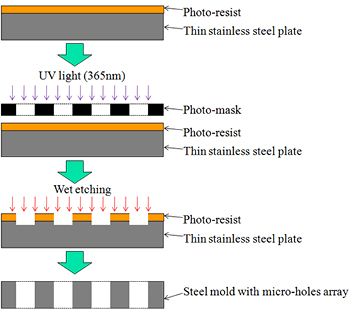
Figure 1. The procedure of fabricating the thin stainless steel mold with the micro-holes array.
Download figure:
Standard image High-resolution image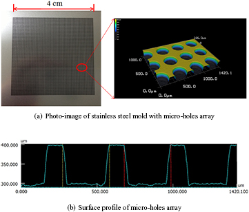
Figure 2. Photo-image and surface profile of the micro-holes array on the thin stainless steel mold.
Download figure:
Standard image High-resolution image2.2. The ultrasonic assisted hot embossing facility and process
After the thin stainless steel mold with micro-holes array is obtained, the ultrasonic assisted hot embossing process was used to fabricate of microlens array pattern on the transparent plastic substrates. The plastic substrate used in this study was optical PMMA plate (Chi Mei Corporation, Taiwan) with a thickness of 4 mm. It has good weather resistance and high transparency. It can be widely applied for backlight light guide plate (LGP), scanners and lighting advertisement. The glass transition temperature (Tg) and refractive index of the PMMA plate are 105 °C and 1.49, respectively.
Figure 3 shows the ultrasonic assisted hot embossing facility in the experiments. The system mainly consists of a commercial ultrasonic welder with horn, power supply and air compressor. The stack of stainless steel mold and plastic substrate was built into the bottom loading stage. The maximum output power and frequency of the machine were 1500 W and 20 kHz, respectively. The ultrasonic vibration time, embossing pressure and embossing hold time can be controlled.
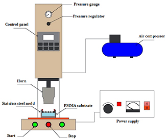
Figure 3. Schematic drawing of the ultrasonic assisted hot embossing facility.
Download figure:
Standard image High-resolution imageFigure 4 shows the procedures of ultrasonic assisted hot embossing for fabrication of plastic microlens array. It can be divided into three steps.
- (a)First, the thin stainless steel mold with micro-holes array is placed on top of the plastic substrate. The stack is put in the bottom loading stage and fixed by screw bolt.
- (b)Then, the horn of the ultrasonic welder comes down to contact the stainless steel mold and plastic substrate. The ultrasonic vibration is applied. During this period, the plastic materials in contact with the mold surface absorb the vibration energy and are heated. The softened polymer flows and fills into the cavities of the mold under a constant pressure. After the vibration stops, the horn holds the plastic substrates against the stainless steel mold for some time for cooling.
- (c)Finally, the horn is pulled back and the plastic substrate releases from the mold. Under the proper processing conditions, the softened polymer material only partially fills the micro-holes of the mold and a convex lens surface is formed due to surface tension. The plastic substrate with microlens array pattern is obtained.

Figure 4. The procedures of ultrasonic assisted hot embossing for fabrication of plastic microlens array.
Download figure:
Standard image High-resolution image3. Results and discussion
3.1. Investigation of the ultrasonic assisted hot embossing process
To verify the feasibility and uniformity of ultrasonic assisted hot embossing process, pressure and temperature distribution during the embossing stage were measured by a pressure-sensitive film and thermocouples. The shape and peak height of embossed microstructures were measured by a surface profiler. As shown in figure 5, nine different measurement points on the PMMA substrate were selected. Figure 6 shows the temperature profiles and processing cycle times of ultrasonic assisted hot embossing and traditional hot embossing. The ultrasonic assisted hot embossing cycle takes only a few seconds, which is shorter than traditional hot embossing process. This would provide significant advantages in terms of a shorter cycle time and improved production efficiency.

Figure 5. Position of the measurement points on the PMMA plate.
Download figure:
Standard image High-resolution image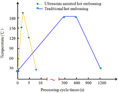
Figure 6. The temperature profiles and processing cycle times of ultrasonic assisted hot embossing and traditional hot embossing.
Download figure:
Standard image High-resolution imageTo study the various processing parameters on the ultrasonic assisted hot embossing of precise micro-lens structures, three processing parameters, i.e. the ultrasonic vibration time, embossing pressure and hold time, were chosen. The values used in the experiments are listed in table 1. By changing one parameter, with other parameters fixed at reference states (underlined in table 1), the effect of each parameter on the quality of micro-lens structures using ultrasonic assisted hot embossing can be determined. Each processing parameter in this study had seven experimental data values. The experimental results and data of average peak height of embossed microstructures were shown in the table 2.
Table 1. The processing conditions used in the experiments.
| Processing Parameters | |||
|---|---|---|---|
| Run | Ultrasonic vibration time (seconds) | Embossing pressure (kgf cm−2) | Hold time (seconds) |
| 1 | 0.5 | 1 | 2 |
| 2 | 1 | 2 | 4 |
| 3 | 1.5 | 3 | 6 |
| 4 | 2 | 4 | 8 |
Table 2. Results of the processing parameter experiments.
| Processing Parameters | Experimental No.:T1 ~ T7 | |||||||||
|---|---|---|---|---|---|---|---|---|---|---|
| (Average Peak height of embossed microstructures under various processing Parameters) | ||||||||||
| Ultrasonic vibration Time (s) | Embossing pressure (kgf cm−2) | Hold time (s) | T1 | T2 | T3 | T4 | T5 | T6 | T7 | Mean (μm) |
| 0.5 | 2 | 4 | 9.6 | 9.9 | 9.8 | 9.9 | 10.1 | 8.6 | 9.1 | 9.6 |
| 1 | 2 | 4 | 39.2 | 39.1 | 39.5 | 39.6 | 39.2 | 39.8 | 40.3 | 39.5 |
| 1.5 | 2 | 4 | 93.5 | 93.2 | 93.6 | 93.7 | 92.9 | 92.8 | 93.9 | 93.4 |
| 2 | 2 | 4 | 99.5 | 99.9 | 100 | 99.8 | 99.7 | 100 | 99.9 | 99.8 |
| 1 | 1 | 4 | 25.9 | 26.1 | 24.9 | 25.6 | 25.8 | 25.4 | 26.2 | 25.7 |
| 1 | 3 | 4 | 44.9 | 46.2 | 45.5 | 45.4 | 44.8 | 46.1 | 45.7 | 45.5 |
| 1 | 4 | 4 | 66.2 | 65.5 | 64.8 | 64.2 | 65.3 | 65.5 | 65.6 | 65.3 |
| 1 | 2 | 2 | 30.2 | 30.5 | 29.5 | 29.8 | 31.2 | 31.6 | 30.5 | 30.5 |
| 1 | 2 | 6 | 44.6 | 43.9 | 45.1 | 43.2 | 42.9 | 43.6 | 43.8 | 43.9 |
| 1 | 2 | 8 | 48.1 | 47.2 | 44.7 | 42.5 | 44.1 | 43.2 | 43.1 | 44.7 |
Note. T1 ~ T7: Average Peak height of embossed microstructures under various processing parameters. The position of the measure points on the PMMA plate was shown in figure 5. T1 ~ T7: (P1 + P2 + P3 + P4 + P5 + P6 + P7 + P8 + P9)/9 Mean = (T1 +T2 + T3 + T4 + T5 + T6 + T7)/7
Figure 7 shows the effect of ultrasonic vibration time on the average peak height of embossed microstructures. When the ultrasonic vibration time was varied from 0.5 to 2 s, the average peak height of the embossed microstructure increases dramatically. This might be due to the fact that during vibration embossing, the surface temperature of plastic substrate increases with ultrasonic vibration time as shown in figure 8. In this experiment, the ultrasonic vibration time was varied from 0.5 s to 3 s while keeping the embossing pressure at 2 kgf cm−2 and hold time at 4 s. When the ultrasonic vibration time is at 0.5 s, the surface temperature of plastic substrate is near 116° C. The polymer material on the surface of the substrate is still rigid and limits the material flow into the mold cavity. The average peak height of the embossed microstructures is only 9.6 μm and no lens shape is formed. At the ultrasonic vibration time of 1 s, the surface temperature of plastic substrate reaches 155° C. The hemispherical micro-lens array pattern on plastic substrate can thus be formed. Figure 9 shows a SEM image of the hemispherical microlens array and its measured result of surface profile. The diameter and sag height of a micro-lens were 250 and 39.5 μm, respectively. When the ultrasonic vibration time is at 1.5 s, the surface temperature of plastic substrate is near 190° C. The average peak height of embossed microstructures is 93.4 μm. The shape and surface profile of the embossed microstructure is shown in figure 10. When the ultrasonic vibration time is at or above 2 s, the surface temperature of the plastic substrate is above 210° C. The plastic material is completely filled into the micro-hole array cavity and forms a micro-cylinder array. The average peak height of the embossed microstructures is 99.8 μm. The only deviation of embossed microstructure from the mold is the peak height and the deviation is less than 0.2%. The shape and surface profile of the embossed micro-cylinder array is shown in figure 11.
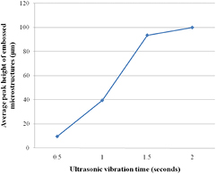
Figure 7. Peak height of embossed microstructures under various ultrasonic vibration times in the process.
Download figure:
Standard image High-resolution image
Figure 8. Surface temperature of plastic substrate under various ultrasonic vibration times in the process.
Download figure:
Standard image High-resolution image
Figure 9. The hemispherical microlens array and its surface profile.
Download figure:
Standard image High-resolution image
Figure 10. Shape of embossed microstructure under ultrasonic vibration time of 1.5 s, with embossing pressure of 2 kgf cm−2 and hold time of 4 s.
Download figure:
Standard image High-resolution image
Figure 11. SEM image of the micro-cylinder array.
Download figure:
Standard image High-resolution imageFigure 12 shows the experimental results recorded by changing the embossing pressure from 1 to 4 kgf cm−2 while keeping the ultrasonic vibration time at 1 s and hold time at 4 s. It is found that the average peak height of the embossed microstructures increased from 25.7 to 65.3 μm. The shape of the embossed microstructure changes from simple hemisphere to cylindrical hemisphere. Typical cylinders with hemispherical profile and their cross-sectional view are shown in figure 13.

Figure 12. Peak height of embossed microstructures under various embossing pressures in the process.
Download figure:
Standard image High-resolution image
Figure 13. SEM of the typical cylindrical microlens array.
Download figure:
Standard image High-resolution imageFigure 14 shows the measured peak heights of the embossed microstructures with respect to the hold time from 2 to 8 s under the embossing pressure of 2 kgf cm−2 and ultrasonic vibration time of 1 s. This experimental result reveals that the average peak height of the embossed microstructure increases with hold time from 2 to 6 s. Further increase of hold time beyond 6 s introduces a very small increase in the peak height of embossed microstructures.

Figure 14. Peak height of embossed microstructures under various hold time in the process.
Download figure:
Standard image High-resolution image3.2. The geometrical uniformity of the plastic microlens array
Based on the above study, a hemispherical microlens array on plastic substrates can be formed at the ultrasonic vibration time of 1 s, with embossing pressure of 2 kgf cm−2 and hold time of 4 s. Figure 15 shows a plastic substrate with 100 × 100 microlens array. It is observed that an array of microlens was successfully fabricated over the plastic substrate. In order to characterize the geometrical uniformity of the plastic microlens array, the ninety microlenses on the PMMA substrate are picked and measured. The position of nine different measure area(P1 ~ P9) was shown in figure 5. Ten microlenses are randomly picked on each area. The diameters of ninety microlenses from a single process run are measured as shown in the figure 16. The average diameter of a microlens was 250.2 μm with a standard deviation of 0.4 μm. The sag heights of microlenses from a single process run are measured as shown in the figure 17. The average sag height of a microlens was 39.5 μm with a standard deviation of 0.3 μm. These results indicate good uniformity and controllability of the ultrasonic assisted hot embossing molded microlenses.

Figure 15. The plastic substrate with 100 × 100 microlens array.
Download figure:
Standard image High-resolution image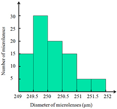
Figure 16. The diameter distribution of a single microlens array.
Download figure:
Standard image High-resolution image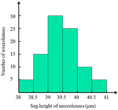
Figure 17. The sag height distribution of a single microlens array.
Download figure:
Standard image High-resolution image3.3. The optical property and surface roughness of plastic microlens array
Under the proper processing conditions, a array of 100 × 100 plastic microlens with a lens diameter of 250 μm, a pitch of 400 μm and a sag height of 39.5 μm has been successfully fabricated. The radius of curvature (R) and focal length (f) of the microlens can be determined using equations based on the basic geometric and optical theory as follows:
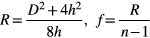
Where D, h and n are diameter, sag height of microlens and the refractive index of the PMMA material (n = 1.49), respectively. The calculated radius of curvature and focal length of the present plastic microlens are 217.5 and 443.9 μm, respectively.
The optical property of the fabricated plastic microlens array is further measured using a beam profiler. The beam profiler is composed of expanding lenses, a filter, a micrometer scale resolution stage, a microscope, a CCD system and a 532 nm laser light source. The measurement result of average focal length is about 440 μm for the fabricated micro-lens with a diameter of 250 μm and a sag height of 39.5 μm. The calculated values agree well with the measured data. Figure 18 shows the focused light spot patterns and normalized intensity of the plastic microlens array. The images reveal that the pitch and the intensity of the focused light spots are uniform. These are significant factors in optical systems.
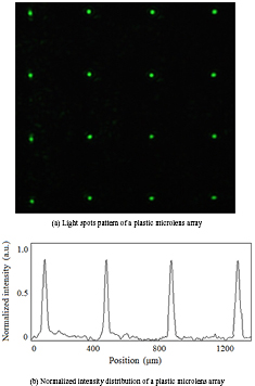
Figure 18. Light spots pattern and intensity profile of a plastic microlens array.
Download figure:
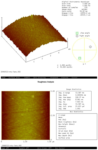
Standard image High-resolution imageTo characterize the surface morphology of the fabricated plastic microlens array, the surface roughness has been measured by an atomic force microscope (AFM). The measurement was performed around the top of a microlens and the measuring area was 5 × 5 μm. The specimen is randomly selected from a single microlens array. Figure 19 shows the AFM image and roughness analysis of a microlens. The average surface roughness (Ra) of a microlens was 7.6 nm. This result reveals that the surface roughness of a plastic microlens array is comparable with that of micro-optical components in practical use.
Figure 19. AFM image and surface roughness of a plastic microlens.
Download figure:
Standard image High-resolution image
4. Conclusions
In this paper, a simple and rapid method for fabricating microlens array on PMMA substrates using an ultrasonic assisted hot embossing process is reported. Under the proper processing conditions, a array of 100 × 100 plastic microlens with a lens diameter of 250 μm, a pitch of 400 μm and a sag height of 39.5 μm has been successfully fabricated. The total cycle time is less than 10 s. The measured surface roughness of the microlens was 7.6 nm. The pitch and intensity distribution of the microlens array are uniform. These results show the potential of the ultrasonic assisted hot embossing process for mass production of microlens arrays with high productivity and low cost. In addition, this effective technology can be extensively applied for microlens fabrication with other plastic materials due to its simplicity and versatility.
Acknowledgments
The National Science Council of Taiwan, R O C under the Grant NSC 102-2221-E-151-016, has supported this work financially. The measurement and technical support from the Center for Micro/Nano Science and Technology (NCKU) is gratefully acknowledged.