
Abstract
In recent years, semi-passive vibration damping using non-linear synchronized switching methods has been intensively investigated and discussed. In this paper, a self-powered synchronized switch damping on inductor (SSDI) technique based on zero-velocity crossing detection is proposed and investigated. The control signal used to drive the switches is obtained by sensing velocity. A totally self-powered damping system powered by harvested energy using the SSDI technique with velocity sensing and without external power is established. Compared with the conventional technique based on voltage peak detector, this technique does not generate lag in detection of switching time. The theoretical model, the experimental evaluation and the drawback of the self-powered zero-velocity crossing detection switching technique are discussed in this study. The system performance is also compared with the externally powered system.
Export citation and abstract BibTeX RIS
1. Introduction
Many successful applications of piezoelectric materials for structure vibration suppression have been developed in recent decades. In these applications, piezoelectric materials convert the vibration energy of the host structure into electrical energy, and then the generated electrical energy is dissipated in a shunt circuit. The piezoelectric shunt techniques were widely used due to their simple configurations and compact size, but these techniques are better if self-powered to reduce the system complexity. In some applications, such as automobiles and aeronautics, the external power is limited [1, 2], and the self-powered design can eliminate the requirement for an external power supply.
There are many shunt techniques used for damping applications. The simplest one is a passive technique that uses a matched inductor and resistor network to the piezoelectric patch [3–5]. The advantages of the passive technique are low cost, easy implementation and inherited stability. However, this technique has a major disadvantage. In low-frequency applications, the optimal shunt inductor is too large for feasible implementation. In most cases, the inductance required would be approximately one hundred henrys, which can only be implemented with active circuitry. To implement a shunt inductance with active circuitry, an external power source is needed, and the major advantage of passive damping is lost. The most effective active-damping technique is to use active controllers, power amplifiers, and analog or digital processors that generate an out-of-phase signal to control the structural vibration. This technique usually provides better damping performance than passive ones [6, 7]. The advantages of the active-damping techniques are good performance and a wider working frequency range, whereas the disadvantage is that the active circuits require external power. The implementation and algorithms for active techniques can be much more complex and the cost is much higher than passive-damping techniques.
Considering the trade-offs in the cost, difficulty of implementation, power consumption required and damping performance, some switch shunting or semi-passive techniques [8–10] have proven to be effective methods. Several switching shunt circuit topologies and corresponding switching laws were proposed. The two most popular switching shunt-damping techniques are SSDI (synchronized switch damping on an inductor) [11] and SSDV (synchronized switch damping on a voltage source) [12, 13]. The SSDI technique has attracted more attention because its offers several advantages: it does not require a very large inductor for low frequencies and it is robust to environmental changes. Moreover, this technique needs only low power to operate the switches. Thus, this technique presents the advantages of being self-powered. The fundamental concept of the SSDI technique is to the use the resonance between the piezoelectric clamped capacitance and a shunt inductance during a short time interval to invert the piezoelectric voltage. The switching shunt circuit only turns 'ON' at the extreme of the displacement or at the zero-crossing of velocity to shift the phase of the voltage across the piezoelectric patch.
Several versions of the self-powered SSDI technique have been proposed [14–17]. Niederberger et al in 2006 proposed an autonomous shunt circuit for vibration damping with one piezoelectric patch to generate the switching signal through a low-pass filter [15]. The common and conventional method is based on peak voltage detection [16, 17] using a small energy storage capacitor. The peak detection is made using an envelope detector: a comparison between the envelope and piezoelectric voltage is made with a bipolar transistor. The drawback of this method is the lag in detection of switching time due to the use of the transistor, which degrades the damping performance [18]. The principle of the peak detector method is shown in figure 1(a). Since in the peak method the triggering at the displacement extreme is only optimal in the case of harmonic excitation, different SSDI control laws were proposed [19]. Beside the control law, the switching time is an important parameter for the SSDI technique. M. Neubauer and J. Wallaschek in 2009 have carried out analytical and experimental investigations of the influence of the time lags and switching losses for the SSDI technique performance [20].

Figure 1. (a) Principle of the voltage peak detector method and (b) principle of the zero-velocity crossing detector method.
Download figure:
Standard imageIn this paper, a self-powered SSDI technique based on zero-velocity crossing detection is proposed and investigated. Hereafter this technique in this paper is called SP-SSDI. Based on the self-powered system used in piezoelectric energy-harvesting devices [21], SP-SSDI does not require external instruments. The control signal used to drive the switches is obtained by sensing the velocity, then comparing it to zero. A totally self-powered damping system powered by harvested energy using the SSDI technique with velocity sensing and without external power is established. The concept of the proposed system is shown in figure 1(b).
The paper is organized as follows: sections 2 and 3 summarize the SSDI technique and present the theoretical analysis. Section 4 presents the detailed analysis of the self-powered SSDI based on the zero-velocity crossing detection technique. Section 5 presents the experimental results, which include the time domain evaluation for different excitation levels, the measurement of the efficiency and the system frequency response results. Finally, section 6 concludes the paper.
2. Electromechanical model
The system consists of piezoelectric 3-1 type PZT patches bonded on a host structure. The governing equation of the piezoelectric patches can be represented as equations (1) and (2).


where FP is the external force exerted on the piezoelectric patch, I is the outgoing current generated from the piezoelectric patch,  is the short circuit stiffness, α is the force–voltage coupling factor, CP is the clamped capacitance of the piezoelectric patch, u is the displacement of the system, vP is the piezoelectric voltage and the dot means the time derivative.
The strain distribution in the piezoelectric patch is assumed homogeneous. Using equations (3) and the parameters of the piezoelectric patches described in table 1, CP,α and  are calculated as:

The coordinates indices (1, 2, 3) are represented in figure 3. A mechanical model based on a spring–mass system gives a good description of the vibration behavior near the resonance of the host structure as shown in figure 2. Therefore, for simplicity, this system can be modeled as a one degree-of-freedom system of a mass M, a spring  and a damper D. According to the dynamics equation, the differential governing equation of this electromechanical system can be expressed as equations (2) and (4):

Table 1. Piezoelectric physical parameters.
| w | Width of the piezoelectric patches |
| t | Thickness of the piezoelectric patches |
| l | Length of the piezoelectric patches |

|
Elastic rigidity of equivalent patches in short circuit |
| e31 | Permittivity of piezoelectric patches |

|
Piezoelectric coefficient of equivalent patches |
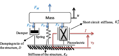
Figure 2. Equivalent mechanical model of piezoelectric and structure.
Download figure:
Standard image3. SSDI technique
The electrical circuit of the semi-passive-damping technique called SSDI (synchronized switching damping on an inductance) is represented in figure 3(a). An inductor L, a resistance R and a switch K are connected in series with the piezoelectric patch. The piezoelectric patch voltage vP1 is switched across the LR shunt circuit. The dissipated energy of the structure depends on the voltage amplitude across the piezoelectric patches. The role of these additional patches is to increase the amplitude of voltage vP1 and thus to increase the damping effect. The switch K is turned ON when a maximum of displacement u occurs and the voltage vP1 starts to oscillate, until K is turned OFF. The switching ON period is equal to a half of the resonant period of the LCP1 circuit. Assuming that the electrical resonant period is very small compared to the mechanical vibration period, voltage vP1 can make the inversion in this short period. The same function can be obtained by turning switch K ON at the minimum displacement. Theoretical waveforms of the displacement u, the velocity  and the voltage vP1 of the SSDI technique are shown in figure 3(b). The amplitude of voltage vP1 is limited by the loss of energy during the inversion process.
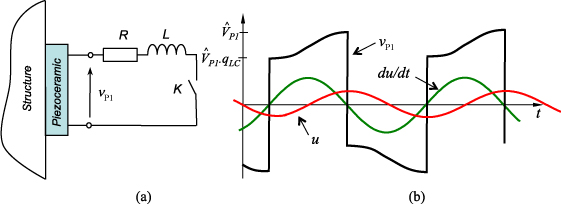
Figure 3. (a) Electric circuit of the SSDI technique. (b) Key waveforms of the SSDI technique.
Download figure:
Standard imageThe absolute value of the voltage of the piezoelectric patch after inversion is less than the initial voltage. This difference occurs because of the energy losses that occur due to the energy flow between the capacitance and the inductor during the switching interval. The absolute value of the inverted voltage is qLCvP1, where  is a function of the quality factor QLC of the resonant LCP1 circuit.
An analytic calculation of the displacement amplitude at resonance ωr can be made from the previously expressed equations. The expression of the mechanical displacement umax as a function of force amplitude FM and the resonant circuit factor qLC is given in equation (5),
4. Self-powered zero-velocity crossing detection for SSDI technique
Due to the use of switches in the SSDI technique, the shunt circuit requires an external power source. To design a totally self-powered device, a part of the extracted energy for damping can be used to power the electronics. Moreover, because it is a synchronous technique, the displacement or the velocity must be measured accurately to obtain the driving signal for the switches. The technique proposed here is to divide the piezoelectric patches into three parts. The largest part, called P1, behaves like the conventional piezoelectric patch used in the SSDI technique to dissipate the vibration energy. The second piezoelectric patch, called P2, is a smaller patch that works like energy-harvesting device to provide power supply to the other electronic circuit. The third piezoelectric patch, called P3, is a smaller patch designed to sense the velocity and to generate a driving signal to control the switches at the optimal time. All three patches contribute to damping the structure.
A schematic of the complete electronic circuit is shown in figure 4 with the functions of different sub-circuits labeled in the same figure. The system will be analyzed in detail in the following subsection. To obtain a precise velocity signal, P3 is cut from the electrode of the lower piezoelectric patch, and the patch is positioned on the centerline of the cantilever, as shown in figure 4.

Figure 4. Schematic diagram of the zero-velocity crossing detection self-powered SSDI technique.
Download figure:
Standard image4.1. Zero-velocity crossing detector (piezoelectric patch P3)
Figure 5 shows the electric circuit and the theoretical waveforms of the zero-velocity crossing detector. Since the mechanical current in the electric equivalent circuit of a piezoelectric patch can be assumed to be velocity; if the output terminal is short circuited, the current through this short circuit is proportional to velocity, i.e.  . To convert this current into voltage, this short circuit can be made by a small resistance. Thus, voltage across the shunt resistance represents the velocity of the structure. The value of the current-sensing resistance must be much smaller than the output impedance of the piezoelectric patch. As shown in figure 5(b), the velocity signal (black curve) is in phase with the output current (green curve). To avoid the noise problems when SSDI is active, a low-pass filter is necessary, because the voltage inversion introduces high-frequency vibrations into the system. A third-order low-pass filter is used; it is composed of two capacitors and an inductor. The design goal of the filter is to ensure that the high-frequency noise is reduced sufficiently to generate an accurate control signal with minimum phase lag to keep the efficiency of the SSDI system. Finally, the filter output voltage vs is connected to a comparator, and the output of the comparator vCout is used to drive the switches, as shown by the red curve in figure 5(b).
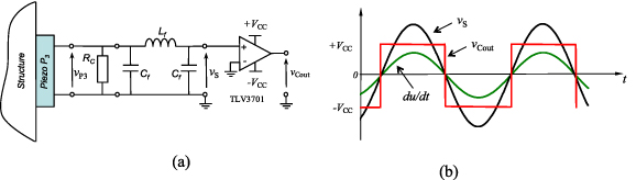
Figure 5. The zero-velocity crossing detector: (a) electric circuit and (b) theoretical waveforms.
Download figure:
Standard imageCompared to the conventional switching method using a voltage peak detector, the velocity-synchronized signal should theoretically cause the switches to switch more precisely at the optimal time. Because the conventional peak detector uses the diode drop to detect the peak voltage, it produces a time lag between the peak time and the switching time.
Figure 6 shows the Bode diagram of the filter of the zero-velocity crossing detector, as measured by an SR780 dynamic signal analyzer. The Bode diagram shows that the corner frequency is approximately 340 Hz. The first natural frequency of the cantilever beam is approximately 34 Hz; approximately ten times lower than the corner frequency of the low-pass filter. The low-pass filter design reduces the high-frequency noise of the velocity signal effectively without altering the phase.
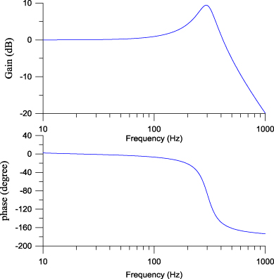
Figure 6. Bode diagram of the filter of the zero-velocity crossing detector.
Download figure:
Standard image4.2. Power supply (piezoelectric patch P2)
Figure 7 shows the electric circuit and the theoretical waveforms of the power supply part. This circuit provides two DC voltages sources, VCC and −VCC, to supply power to the comparator and the switches of the SSDI circuit. The power supply circuit is composed of two diodes (DA and DB) and three capacitors (CP,CN and Cr). The two diodes maintain the correct positive and negative current flows to charge the capacitors. CP regulates the positive voltage between VCC and ground, while CN regulates the negative voltage between −VCC and ground. Cr regulates the voltage between VCC and −VCC, and acts as an energy storage buffer. Two Zener diodes DZ are used to limit excursion and to regulate the DC voltage. The two regulated voltages, VCC and −VCC, are connected to the comparator, and the output of the comparator is used to drive the switches. The comparator used in this application is a Nanopower comparator TLV3701 from Texas Instrument (Dallas USA) that sinks a small and constant current (IComp = 560 nA) for a voltage VCC higher than 2.5 V. Assuming that the equivalent load of the comparator between the two regulated voltages is Req = 2 VCC/IComp, the voltage VCC can be expressed as in equation (6) [22].

Using equation (3) giving the relation between α,CP2 and the parameters of the piezoelectric patches, the voltage VCC can be rewritten as equation (7):
Since voltage VCC must be higher than 2.5 V, we can find a relation between the amplitude of displacement and the size of piezoelectric patch P2, as shown in equation (8):

Equation (8) must be used to design piezoelectric patch P2. This relation gives minimal dimensions of the patch P2 to be sure that SSDI interface will work correctly for a small displacement.

Figure 7. Power supply circuit: (a) electric circuit diagram and (b) key waveforms.
Download figure:
Standard image5. Experimental results and discussion
5.1. Experimental setup
Figure 8 shows the experimental setup and pictures of the zero-velocity crossing based SSDI damping system. The experimental structure is a cantilever steel beam with three 31 type PZT-QA patches provided by the Eleceram Technology Co., Ltd (Taoyuan Taiwan). The fixed end of the beam is excited by a shaker (Bruel and Kjaer 4809), and the shaker-driving signal is generated by a DAQ card (NI USB-6259 from National Instrument, Austin USA) on a notebook computer. A vibrometer (LK-G3001P + LK-G32 from Keyence, Osaka Japan) is used to measure the beam tip displacement, and an accelerometer (Brüel and Kjaer 4381 from Brüel and Kjær Sound and Vibration Measurement A/S, Nærum Denmark) is used to measure the acceleration at the fixed end. The piezoelectric voltage, the displacement and the acceleration are recorded by the DAQ card. The dimensions of the cantilever beam and the piezoelectric patches are shown in table 2. The component measured values and model parameters are shown in table 3. The first natural frequency of the cantilever beam is 34 Hz. The dimension and the clamped capacitance of the main piezoelectric patch are much greater than those of the two small piezoelectric patches.
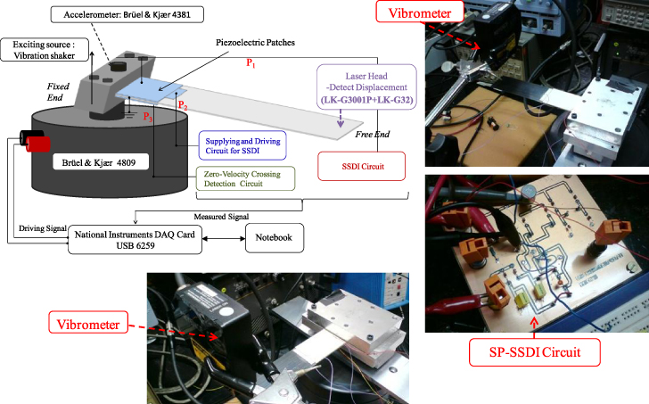
Figure 8. Experimental setup and pictures.
Download figure:
Standard imageTable 2. Dimensions of the piezoelectric patches.
| Steel beam | Length × width × thickness | 140 mm × 35 mm × 0.5 mm |
|---|---|---|
| Piezoelectric patches | P1 | 50 mm × 65.5 mm × 0.6 mm |
| P2 | 30 mm × 5 mm × 0.5 mm | |
| P3 | 50 mm × 4.5 mm × 0.6 mm |
Table 3. Component values and model parameters.
| Symbol | Description | Value (unit) |
|---|---|---|
| E | Young's modulus of the steel beam | 210 GPa |
| ρ | Density of the steel beam | 7850 kg m−3 |
| fop | Open circuit resonant frequency when all piezoelectric patch is in open circuit | 34 Hz |
| fsh | Short circuit resonant frequency when all piezoelectric patch is in short circuit | 33.97 Hz |
| k2 | Electromechanical coupling coefficient | 0.0018 |
| ζ | Damping ratio | 0.02 |
| QM | Mechanical quality factor | 2.09 |
| M | Mass | 28 g |
| KE | Equivalent stiffness when all piezoelectric patch is in short circuit | 1276 N m−1 |
| KD | Equivalent stiffness when all piezoelectric patch is in open circuit | 1278 N m−1 |
| D | Damping coefficient | 0.24 N m−1 s−1 |
| αP1 | Force–voltage factor of P1 | 0.000 368 N V−1 |
| αP2 | Force–voltage factor of P2 | 0.000 0242 N V−1 |
| αP3 | Force–voltage factor of P3 | 0.000 0227 N V−1 |
| QLC | Quality factor of resonant L–CP1 | 4.4 |
| R | Equivalent resistor of resonant L–CP1 | 0.48 Ω |
| qLC | Inversion factor | 0.7 |
| CP1 | Clamped capacitance of P1 | 67.6 nF |
| CP2 | Clamped capacitance of P2 | 4.44 nF |
| CP3 | Clamped capacitance of P3 | 4.16 nF |
| L | Resonant inductor in SSDI | 10 mH |
| Cr | Regular capacitor in supply circuit | 4.7 μF |
| CP | Regular capacitor in supply circuit | 2.2 μF |
| CN | Regular capacitor in supply circuit | 2.2 μF |
| DZ | Zener diode in supply circuit | 15 V |
| Lf | Low-pass filter inductor in zero-velocity crossing detector | 700 mH |
| Cf | Low-pass filter capacitor in zero-velocity crossing detector | 470 nF |
5.2. Experimental results
Experimental data were taken to validate the self-powered velocity-synchronized semi-passive system presented in this paper and to demonstrate the operation of the circuit.
Figure 9 shows the displacement, the sensed velocity, the switching signal and the piezoelectric voltage of uncontrolled and self-powered SSDI systems for an acceleration of 0.16 m s−2. Comparing the results with and without the SSDI system active, the tip displacement is reduced from approximately 1.12 to 0.72 mm by the SSDI damping effect. Because the current-sensing resistance of 1 kΩ is much lower than the output impedance of the piezoelectric patch, the signal is very small, with a peak value of approximately 0.01 V. When SSDI is active, the high-frequency noise is easily introduced into the velocity control signal, but it does not influence the power supply effectiveness because the capacitors in the rectifier regulate the supplied voltage.

Figure 9. Experimental results of the zero-velocity crossing detection circuit (a) without SSDI active and (b) with SSDI active (green trace: velocity VS, black trace: VCout, blue curve: piezoelectric voltage VP, and red trace: beam tip displacement u).
Download figure:
Standard imageThe operating limit of the self-powered technique is obtained when the voltage VCC is lower than 2.5 V. Once the SSDI circuit works, the decrease of the vibration magnitude leads to a decrease in terms of harvested power and, thus, to a decrease of voltage VCC. Therefore there is a minimum value of the displacement magnitude. In figure 9 we can see that the DC voltage VCC is equal to 3.26 V for a displacement of 1.12 mm, and 2.51 V for a displacement of 0.72 mm. The experimental limit of the system is 0.7 mm to have VCC greater than 2.5 V to power the comparator in the circuit. Figure 10 shows the theoretical and experimental value of VCC as a function of displacement.
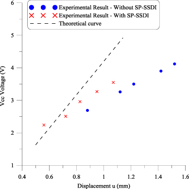
Figure 10. Voltage VCC as a function of displacement u.
Download figure:
Standard imageThis minimum value of the displacement magnitude can be set by the size of the piezoelectric patch P2. If we consider the thickness is fixed and vary the width, equation (8) can be used to predict the minimal displacement magnitude required for the corresponding width. The theoretical minimum value of magnitude of displacement as a function of the width is therefore plotted in figure 11 for thickness t = 0.5 mm and length l = 30 mm. Figure 11 shows that for a width w = 5 mm, the theoretical value of the displacement magnitude is 0.7 mm.

Figure 11. Minimum value of displacement magnitude as a function of the width of piezoelectric patch P2.
Download figure:
Standard image5.3. Comparison
For comparison, experiments were carried out in four different cases; these cases are listed in table 4.
- Case 1 is the reference case, used to show the undamped situation. The piezoelectric voltage is in phase with the tip displacement and has a phase lag of approximately 90° with respect to the velocity signal.
- Case 2 is the maximal damping condition. All three piezoelectric patches (P1 + P2 + P3) are controlled using the SSDI damping technique, and the SSDI is operated by external instruments. The power source is an external DC power supply, and the optimal switching signal is provided by a function generator.
- Case 3 provides an experimental control for comparison with case 4. In case 3, only one piezoelectric patch (P1) is controlled using the SSDI damping technique. The power source is an external DC power supply, and a function generator provides the switching signal.
- Case 4 is the experimental condition and uses the self-powered technique (SP-SSDI) presented in this paper without any external instruments.
Table 4. Four experimental cases.
| Piezoelectric patches | Conditions | |
|---|---|---|
| Case 1 | Uncontrolled | |
| Case 2 | P1 + P2 + P3 | External energy: power supply |
| Optimal switching point: function generator | ||
| Case 3 | P1 | External energy: power supply |
| Optimal switching point: function generator | ||
| Case 4 | P1 | No external energy. Using self-powered supplying circuit. |
| Switching point: velocity control circuit. |
The following two subsections will compare the damping performance of each of the cases when the beam is driven at different excitation levels. The results will be compared in both the time domain and the frequency domain.
5.3.1. Time domain comparison.
The cantilever beam is driven at its first natural frequency (34 Hz) at different accelerations. Figures 12 and 13 show the experimental results of the displacement and the work cycles calculated for the four cases for accelerations of 0.13 m s−2 and 0.16 m s−2, respectively. To quantify the performances of damping technique, the force–displacement diagram (work-cycle) is employed to illustrate the energy conversion cycle. In the case of a purely capacitive load on the piezoelectric patch (case 1), the displacement and voltage are in phase; the area of the cycle is null, so the extracted energy is equal to zero. When the SSDI technique is active, the LCP resonance circuit increases the magnitude of voltage vP and decreases the displacement u. The area of the cycle is the extracted energy. Case 2 is the most effective one because all piezoelectric patches are used for the damping control with the SSDI technique. This is the ideal experimental case because the SSDI circuit is powered by an external power supply. If we compare case 3 (external drive) and case 4 (self-powered), we obtain a good evaluation of the zero-velocity crossing detection technique (same area of piezoelectric patches with SSDI). For an acceleration of 0.13 m s−2, the self-powered SSDI circuit damps the structure only up to 0.7 mm (0.5 mm for the case with external supply) due to the limit of operation of the comparator. For an acceleration of 0.16 m s−2 and higher, the results show that the amplitude of voltage and displacement are in phase, which means that with the proposed technique the switching occurs at nearly the optimal time. The little difference is due to the high-frequency noise in the velocity sensing signal.

Figure 12. Experimental results (acceleration = 0.13 m s−2) (a) displacement, (b) work-cycle.
Download figure:
Standard image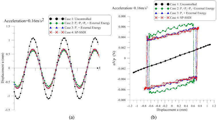
Figure 13. Experimental results (acceleration = 0.16 m s−2) (a) displacement, (b) work-cycle.
Download figure:
Standard imageFigure 14 shows the experimental results and theoretical values of the displacement magnitude as a function of acceleration. The self-powered technique operates successfully for accelerations higher than 0.16 m s−2. For lower accelerations, the damped displacement is kept at 0.7 mm until the uncontrolled displacement is higher than 0.7 mm. The system behaves like a feedback control loop; SSDI decreases the displacement, but when the displacement is lower than 0.7 mm the comparator stops working and the displacement increases again.

Figure 14. Displacement magnitude as a function of acceleration.
Download figure:
Standard imageTable 5 summarizes the experimental results for 4 accelerations: 0.16, 0.19, 0.21 and 0.24 m s−2. The tip displacement increases as the imposed acceleration increases. Two measures of efficiency are proposed and defined in equations (9) and (10); there are presented in table 5. The first efficiency compares the self-powered technique with velocity control, called SP-SSDI here, to the use of all of the piezoelectric patches (P1 + P2 + P3) for SSDI damping. From table 5, the average efficiency is approximately 86%. This result means that if the size of the piezoelectric patches used in the system is not increased, the proposed SP-SSDI technique provides approximately 14% less damping. The second efficiency compares the SP-SSDI technique to the case in which only the P1 patch is used for SSDI, and the patch is controlled with an external function generator with perfect timing and powered by external power sources. This measure provides a fairer comparison because the area of the piezoelectric patch used for the SSDI is the same as that used for the self-powered system. From table 5, the average of this efficiency measure is approximately 95%. This means that the phase lag generated by the inherent structure and the passive low-pass filter degrades the damping performance by approximately 5%. Based on the two comparisons, the SP-SSDI technique demonstrates high efficiency and good damping ability while maintaining a fully self-powered system.


Table 5. Experimental results for different excitation levels.
| Acceleration (m s−2) | Tip displacement (mm) | Efficiency1 (%) | Efficiency2 (%) | |||
|---|---|---|---|---|---|---|
| Case 1: uncontrolled | Case 2: P1 + P2 + P3 | Case 3: P1 | Case 4: SP-SSDI | |||
| 0.16 | 1.12 | 0.65 | 0.7 | 0.72 | 85.11 | 95.24 |
| 0.19 | 1.23 | 0.75 | 0.81 | 0.825 | 84.38 | 96.43 |
| 0.21 | 1.42 | 0.86 | 0.917 | 0.95 | 83.93 | 93.44 |
| 0.24 | 1.52 | 1.013 | 1.039 | 1.066 | 89.55 | 94.39 |
| Average | 85.74 | 94.87 | ||||
Figure 15 shows the experimental results in the time domain at an acceleration of 0.19 m s−2. The results show that when the SP-SSDI system starts to take effect, the tip displacement decreases rapidly, and the piezoelectric terminal voltage increases rapidly. The results also demonstrate that the SP-SSDI system provides good, stable damping during the period when it is active. The SSDI damping effect is not influenced when the self-powered system is active.

Figure 15. Experimental results in the time domain of the self-powered technique.
Download figure:
Standard image5.3.2. Frequency response.
Figure 16 shows the frequency responses of the system for the four cases and for accelerations of 0.13, 0.16, 0.21, and 0.24 m s−2. The testing frequency ranges from 28 to 40 Hz. For an acceleration of 0.13 m s−2, we can see clearly the limit of the system; the SSDI circuit damps the structure only up to 0.7 mm, it is not very effective. As we say, the system works like a feedback control loop and regulates displacement at 0.7 mm. When the uncontrolled displacement is lower than 0.7 mm the SSDI is not active. An acceleration of 0.16 m s−2 is the limit case; the damped displacement is 0.7 mm with the self-powered technique (case 4) and with an external supply (case 3), but the bandwidth is smaller with the self-powered technique (2 Hz). For accelerations of 0.21 and 0.24 m s−2, the self-powered technique provides almost the same damping ability as the case in which the P1 patch is controlled with external instruments. The working bandwidth of the self-powered system is approximately 3.5 Hz at 0.21 m s−2 acceleration, and 3.5 Hz at 0.24 m s−2 acceleration. Compared to the cases in which the P1 + P2 + P3 patches and the P1 patch are driven by external instruments (with working bandwidths of approximately 5 Hz and 6 Hz, respectively), the self-powered technique does not provide as much damping. Consequently, when the exciting acceleration is low, the working bandwidth is small. However, when the exciting acceleration is sufficiently high, the working bandwidth is almost the same as when external instruments are used.
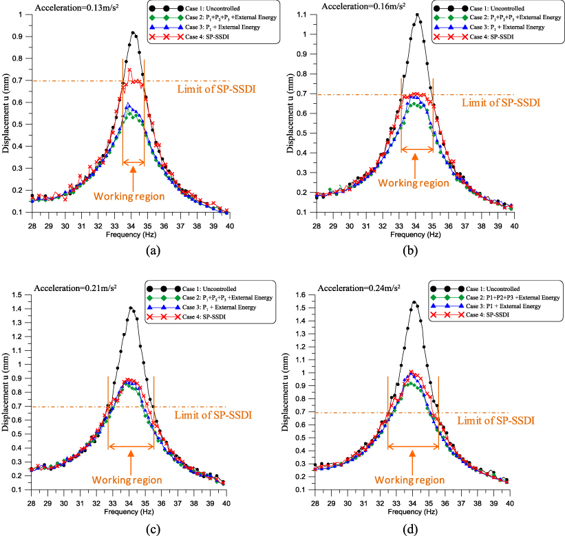
Figure 16. Experimental frequency response results: (a) acceleration = 0.13 m s−2, (b) acceleration = 0.16 m s−2, (c) acceleration = 0.21 m s−2, and (d) acceleration = 0.24 m s−2.
Download figure:
Standard image6. Conclusions
In this study, a self-powered SSDI technique based on the zero-velocity crossing detection is proposed. The control signal used to drive the switches is obtained by sensing the velocity, which is demonstrated to have the best damping performance. The self-powered system concept is to divide the piezoelectric patch into three patches. The largest patch behaves like the conventional piezoelectric patch used in the SSDI technique to dissipate the vibration energy. The second piezoelectric patch is a smaller patch that works like an energy harvester to provide the power supply circuit. The third piezoelectric patch is also a smaller patch designed to sense the velocity and to generate a driving signal to control the switches. Compared to the case in which all of the piezoelectric patches (P1 + P2 + P3) are used for structural damping and driven by an external function generator and a power supply, the efficiency of the proposed self-powered system is approximately 86%. Compared to the ideal switching case in which only the main piezoelectric patch is used for SSDI damping and is driven by an external function generator and power supply, the efficiency of the proposed self-powered system is approximately 95%. The results show that in the proposed technique it is only necessary to sacrifice a small amount of damping performance to make the system fully self-powered. Furthermore, the circuit design and the implementation of the proposed technique are quite simple, and thus the proposed technique is a promising design compared with the other self-powered damping techniques.
Acknowledgments
The authors are grateful to Eleceram Technology Co., Ltd for providing piezoelectric patches used in this research work. The funding support from National Science Council, Taiwan under Project NSC-98-2221-E-002-139-MY2 is gratefully acknowledged.