Abstract
Polymer-based photovoltaic devices have the potential for widespread usage due to their low cost per watt and mechanical flexibility. Efficiencies close to 9.0% have been achieved recently in conjugated polymer based organic solar cells (OSCs). These devices were fabricated using solvent-based processing of electron-donating and electron-accepting materials into the so-called bulk heterojunction (BHJ) architecture. Experimental evidence suggests that a key property determining the power-conversion efficiency of such devices is the final morphological distribution of the donor and acceptor constituents. In order to understand the role of morphology on device performance, we develop a scalable computational framework that efficiently interrogates OSCs to investigate relationships between the morphology at the nano-scale with the device performance.
In this work, we extend the Buxton and Clarke model (2007 Modelling Simul. Mater. Sci. Eng. 15 13–26) to simulate realistic devices with complex active layer morphologies using a dimensionally independent, scalable, finite-element method. We incorporate all stages involved in current generation, namely (1) exciton generation and diffusion, (2) charge generation and (3) charge transport in a modular fashion. The numerical challenges encountered during interrogation of realistic microstructures are detailed. We compare each stage of the photovoltaic process for two microstructures: a BHJ morphology and an idealized sawtooth morphology. The results are presented for both two- and three-dimensional structures.
Export citation and abstract BibTeX RIS
1. Introduction
The utility of cheap sources of renewable energy in a world faced with dwindling conventional energy sources and climate change is indisputable. Solar radiation is one of the most promising and long term sources of renewable energy. Traditional inorganic solar cells have made significant progress in harnessing this energy, but their high manufacturing cost still prohibits widespread usage. In contrast, organic solar cells (OSCs) permit large-area fabrication (by incorporating facile manufacturing suitable for roll-to-roll processing) which potentially gives a much cheaper source of photoelectric conversion [3]. In addition, compatibility with flexible substrates, high optical absorption and easy tunability by chemical doping [4] make OSC devices even more attractive for versatile applications at large (solar farms, exterior walls of buildings) as well as small (garments, umbrellas, handbags [5]) scales.
In recent years, we have witnessed significant improvement in efficiencies (from below 3% [6] to the current highest reported value of 9.0% [1] obtained under laboratory conditions). New materials development [7–9], and device designs [10–12] are largely responsible for this improvement. Tailoring the morphology of the active layer will have a significant effect on the final performance of the device, as suggested by experimental evidence [13–16]. For instance, efficiency gains have been reported by changing the morphology using a higher boiling point solvent [6] during processing, annealing [17] at a temperature above the glass transition of the polymer and by making use of additives [18, 19]. Still, compared with inorganic devices, polymer devices have very low efficiency which can be significantly improved by tuning the morphology [17].
High-throughput experiments to test (and tune) devices with various morphologies is time consuming, resource intensive and prohibitively expensive. A computational framework which can efficiently interrogate the microstructure by capturing the physics of charge generation and transport in OSCs will be immensely helpful in understanding the effect of morphology on performance, thus allowing the design of high efficiency solar cells. Broadly, there are two classes of computational models used to interrogate heterogeneous semiconductor devices: microscopic and continuum models.
Microscopic models (Monte Carlo technique and derivatives) [20–22] have been used successfully to determine the effect of morphology on generation, recombination and transport of excitons and charges. These methods have been used to delineate and understand the various sub-processes in semiconductor analysis [23, 24]. However, these methods have some significant drawbacks. In particular, the computational cost involved with three-dimensional simulations and high-throughput analysis (for morphology characterization) is prohibitive. In addition, the long range nature of Coulomb interaction limits the use of microscopic models [25] when full device simulations are needed.
Continuum models provide a computationally efficient alternative to microscopic models. Continuum models based on excitonic drift–diffusion equations for heterogeneous microstucture have been considered by Barker et al [26], Buxton and Clarke [27], Martin et al [28], Walker and Williams [25] and Shah and Ganesan [29]. The excitonic drift–diffusion model is obtained by adding an additional exciton diffusion equation to the standard current-continuity and Poisson equations, i.e. the standard drift–diffusion model. The drift–diffusion model is derived from the Boltzmann transport equation by replacing actual carrier distribution function with equilibrium distribution function assuming the charge carrier temperature to be constant throughout the device [30]1. We note that the utility of the continuum model hinges on the accurate representation of dissociation, recombination processes and mobilities. However, a scalable and efficient implementation of the continuum model will allow rapid classification and approximate rank ordering necessary for high-throughput analysis2. In addition, a continuum model will facilitate investigation of various long range interactions and testing of different models for the sub-processes.
Our contributions in this paper are as follows: (1) We extend the excitonic drift–diffusion model which was successfully applied to organic semiconductor devices with regular microstructures [25–29]. (2) We implement a parallelized finite element framework to efficiently interrogate device scale morphologies. (3) We investigate the electrical properties of realistic interpenetrating heterogeneous microstructures. (4) We characterize the effects of the interfacial area on each stage of current generation process. (5) We perform a stage-by-stage comparison of a percolating and an idealized sawtooth microstructure.
2. Problem definition
2.1. Device morphology
Figure 2 shows a typical configuration of an OSC. The active layer comprised of a blend of donor and acceptor materials forms the domain under consideration. Figure 1 shows the structure of the active layer as seen under a transmission electron microscope [32]3. The top and bottom boundaries are connected to electrodes. Typically, the anode is transparent to the visible region of radiation spectrum, while the metallic cathode is reflective4.

Figure 1. (a) Morphology of the active layer for a typical donor–acceptor system imaged using TEM [32]. Dimensions are 1200 nm × 100 nm.
Download figure:
Standard image
Figure 2. Schematic of the cross-section of a typical OSC device along the thickness.
Download figure:
Standard image2.2. Device physics
The active layer of OSC devices (figure 2) consists of a blend of electron donor and electron acceptor materials. The current generation process in OSCs can be broadly divided into three stages. Stage 1—exciton generation and diffusion: the absorption of light resulting in the generation and subsequent diffusion of tightly coupled electron–hole pairs known as excitons toward the DA interface. Stage 2—charge generation: the excitons then separate at the interface to form electrons in the acceptor region and holes in the donor region. Stage 3—charge transport: the movement of electrons and holes toward the cathode and anode, respectively. Each stage is described in detail as follows.
Stage 1. The electron donor in the active layer of the OSCs absorbs the photons reaching it through the transparent electrode. Unlike inorganic photovoltaic devices, where the absorbed photons directly create free electron–hole pairs, organic photovoltaic devices give rise to tightly bound electron–hole pairs known as excitons [17] (figure 3(a)). These excitons, which have a short lifetime of ∼0.5 ns nanoseconds [31], must diffuse to the donor–acceptor interface in order to be separated into free charges.

Figure 3. Device operation. (a) Photon absorption/exciton generation. (b) Exciton diffusion and charge separation. (c) Free charge creation and transport.
Download figure:
Standard imageStage 2. At the interface, [33] the difference in the electron affinity of the materials causes the electron in the exciton to jump to the acceptor (figure 3(b)). The hole remains in the donor region. This transfer of electron causes the electron–hole pair to become loosely bound. The loosely bound electron and hole can be separated by the local electric field at the interface.
Stage 3. Once the exciton has separated into a free electron and a hole in the two regions across the interface, the charges travel to the electrodes through the respective materials. That is, the electron is transported through the acceptor-rich region toward the anode, while the hole is transported through the donor-rich regions toward the cathode (figure 3(c)). The transport characteristics are affected by the local electric field [17]. The tortuous structure of the pathways (see figure 1) makes transport of the generated charges toward the electrodes a complex process.
2.3. Device model
The equations describing the charge transport processes in a heterogeneous OSC are given below. The four fields of interest are the electron density n, hole density p, electrostatic potential φ and exciton density X.


where the Poisson equation (equation (1)) incorporates the effect of electron and hole densities on potential φ in the active layer.  is the dielectric constant, and is a spatially varying field. Equations (2), (3) are commonly known as the current-continuity equations. The notations for electron and hole current densities are Jn and Jp, respectively. The exciton generation, diffusion and dissociation are represented by equation (6).
 and
and
![$\mathcal{D}_{[\nabla\phi,X]}$](https://content.cld.iop.org/journals/0965-0393/20/3/035015/revision1/msmse403725ieqn002.gif) denote rate of exciton generation and dissociation, respectively. Exciton relaxation rate is denoted by
denote rate of exciton generation and dissociation, respectively. Exciton relaxation rate is denoted by
![$\mathcal{R}_{[X]}$](https://content.cld.iop.org/journals/0965-0393/20/3/035015/revision1/msmse403725ieqn003.gif) .
.
Remark 1: Donor–acceptor interface. The exciton dissociation
and charge recombination
![$\mathcal{R}_{[n,p]}$](https://content.cld.iop.org/journals/0965-0393/20/3/035015/revision1/msmse403725ieqn004.gif) are confined to a thin region at the DA interface using the factor f. This is similar to the boundary condition for excitons at the interface, used by Martin et al [28]. The factor f takes a value of one in the thin region (∼2 nm thick) across DA interface which is used to approximate the interfacial region. f is zero elsewhere. This finite interfacial region allows transport of both electrons and holes but the electrons are restricted to acceptor regions (and holes to donor regions) using a mobility value 20 orders of magnitude lower than the mobility in acceptor regions (donor regions in case of holes).
are confined to a thin region at the DA interface using the factor f. This is similar to the boundary condition for excitons at the interface, used by Martin et al [28]. The factor f takes a value of one in the thin region (∼2 nm thick) across DA interface which is used to approximate the interfacial region. f is zero elsewhere. This finite interfacial region allows transport of both electrons and holes but the electrons are restricted to acceptor regions (and holes to donor regions) using a mobility value 20 orders of magnitude lower than the mobility in acceptor regions (donor regions in case of holes).
The mobilities for electron, holes and excitons are denoted by μn, μp and μX, respectively. The thermal voltage Vt = kBT/q, where kB is the Boltzmann constant, T the temperature and q denotes elementary charge. The Onsager dissociation rate [26]
 is given by

In this expression Eb = q2/(4πx) is the exciton binding energy,
 is the field parameter and J1 is the first order Bessel function given by

The charge recombination
![$\mathcal{R}_{[n,p]} = \gamma np$](https://content.cld.iop.org/journals/0965-0393/20/3/035015/revision1/msmse403725ieqn007.gif) , where γ is the Langevin recombination parameter. In this study, the following form for Langevin parameter
, where γ is the Langevin recombination parameter. In this study, the following form for Langevin parameter
 [2] is used. The exciton relaxation
![$\mathcal{R}_{[X]} = X/\tau_X$](https://content.cld.iop.org/journals/0965-0393/20/3/035015/revision1/msmse403725ieqn009.gif) [2], where τX is the average lifetime of an exciton. Generation rate of excitons is given by
[2], where τX is the average lifetime of an exciton. Generation rate of excitons is given by
![$\mathcal{G}_{[x]}=\alpha_0\Gamma_0 {\rm exp}(-\alpha_0x)$](https://content.cld.iop.org/journals/0965-0393/20/3/035015/revision1/msmse403725ieqn010.gif) , where α0 is the absorption coefficient, Γ0 the photon flux, and x is the distance from the top of the active layer which is in contact with the transparent electrode.
, where α0 is the absorption coefficient, Γ0 the photon flux, and x is the distance from the top of the active layer which is in contact with the transparent electrode.
Remark 2. Boundary conditions. Assuming that the cathode and anode line up with the conduction and valence band, respectively, the boundary conditions [34, 35] for the charge densities are given by
for the cathode, and
for the anode. Here, Egap is the band gap and NC, NV denote the effective density of states of conduction and valence band, respectively. The built-in potential Vbi is given by qVbi = φan − φcat, where φan and φcat are the work functions for the anode and the cathode, respectively. Alignment of electrodes with the conduction and valence bands gives Vbi = Egap. Hence, the boundary condition for potential at the electrodes is given by

where Va is the applied voltage.
Remark 3: Current–voltage plot. The solution of the excitonic drift–diffusion equations (1)–(6) is used to calculate the electron and hole current density vectors using equations (4) and (5)5. The current density available from the device is obtained by integrating the normal component of Jn, Jp at the electrodes. The variation of current density is plotted for a range of applied voltages—zero volts to open-circuit voltage—and is popularly known as the current–voltage characteristic plot.
3. Methodology
In addition to the numerical instabilities due the drift term in current-continuity equations, the highly coupled nature of the equations (1)–(6) makes a computational solution non-trivial. Approximately 20 orders of magnitude variation in the charge distributions (n, and p), and device thickness in nanometers may lead to overflow and underflow errors. Moreover, the large problem size obtained due to the need to resolve the fine morphological details necessitates parallelization in order to be able to perform high-throughput analysis of different microstructures.
This section details the computational approach used to solve equations (1)–(6).
3.1. Non-dimensionalized equations
The use of normalized units helps one to avoid numerical overflow/underflow and improves the efficiency of the algorithms. Using the scaling strategy of Markowich et al [37], the basic equations transform into the following:


where
 denotes non-dimensionalization.
will not be used in the following for notational convenience.
denotes non-dimensionalization.
will not be used in the following for notational convenience.
Finite-element formulation. We use a finite-element formulation to solve this set of equations (12)–(15). The numerical instabilities associated with the presence of drift (convective) term in the current-continuity equations is taken care using the streamline upwind Petrov–Galerkin (SUPG) formulation [38]. The weak form of the problem defined by equations (12)–(15) can be stated as follows.
Given a domain Ω, with boundary ∂Ω, find φ, n, p, X H1(Ω), φ = φD, n = nD, p = pD, X = XD on ∂ΩD such that


for all w H1(Ω), w = 0 on ∂ΩD, where H1(Ω) represents the Sobolev space. φD, nD, pD and XD represent the Dirichlet boundary values for the potential φ, charge densities n and p, and exciton density X, respectively. q* is the SUPG function which modifies the Galerkin test function w to a Petrov–Galerkin test function (w + q*) [38]. On the remainder of the domain boundary ∂Ω/∂ΩD, a zero boundary condition for the normal component of ∇φ, Jn and Jp is implicitly applied.
Discretization. In this stage we replace the infinite-dimensional solution space H1(Ω) with a finite-dimensional approximate Hh(Ω) representing the discrete solution set on a grid. The finite-dimensional counterparts of the solution variables φ, n, p, X are denoted by φh, nh, ph, Xh. The Galerkin form of equations can be stated as follows.
Find φh, nh, ph, Xh Hh(Ω), satisfying the essential boundary conditions such that


for all wh Hh, where φh, nh, ph and Xh are the Galerkin approximations to the electrostatic potential, electron density, hole density and exciton density, respectively. The discretized equations (20)–(23) generate a coupled system of non-linear algebraic equations.
3.2. The computational framework
Overview. Given the microstructural description of the device, the morphological details are mapped onto a computational mesh. This mesh is used by the excitonic drift–diffusion equation solver to obtain the charge density and potential distribution in the device. The current–voltage characteristic curve is post-processed from the results.
Framework setup and domain decomposition. The drift–diffusion equation solver module is implemented in C++ using an in-house parallelized finite-element library which is based on PETSC [39].
Determining the electrical properties of heterogeneous polymer devices with small feature sizes requires fine mesh resolution. Additionally, the relatively large device dimensions (1000 nm × 100 nm) considered in this study results in large degrees of freedom. Furthermore, we need to solve the non-linear excitonic drift diffusion equations at different values of applied voltages in order to obtain the current–voltage characteristic curve. This necessitates parallelization of the framework for quick simulations. We utilize domain decomposition strategy to partition the computational mesh among the processors of a cluster using ParMETIS [40].
Solvers. The non-linear problem is solved utilizing the 'scalable nonlinear equation solver' (SNES) module of the PETSC library. The linear system at each iteration of the non-linear problem is solved using the MUMPS [41] library.
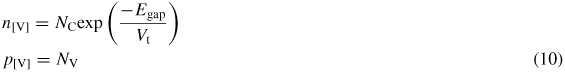
Scaling analysis. We consider a heterogeneous two-dimensional morphology for the timing study. The non-linear excitonic drift–diffusion equations were solved using Newton's method with relative tolerance for convergence set to 10−12. The code was compiled with optimization options for the compiler set on. The timing tests were performed on the 'Cystorm' cluster at Iowa State University which consists of 3200 computer processor cores and high-speed infiniband interconnection.
Figures 4(a) and (b) show the results of the scaling study for different number of degrees of freedom. The plots allow us to determine the optimum number of processors to use for a problem with specific number of degrees of freedom. A problem size of 1.28 million degrees of freedom solved on around 60 processors would result in maximum speedup. These plots (figure 4) show a reduction in solution time with increase in processors used, and this reduction is improved as the problem size increases.
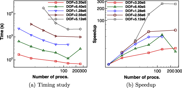
Figure 4. Scaling of the parallelized framework.
Download figure:
Standard imageThe three-dimensional simulations scale similar to their two-dimensional counterparts with some deterioration due to increased bandwidth of the stiffness matrix.
4. Results and discussion
4.1. Realistic heterogeneous morphology
We utilize the computational framework to capture the influence of realistic active layer morphology on the electrical properties of a photovoltaic device. Figure 5(a) shows the vertical cross-section of the active layer of a heterogeneous organic photovoltaic device composed of donor and acceptor materials. The thickness of the active layer is 100 nm. The top and bottom are connected to the anode and cathode, respectively.

Figure 5. Cross-section of the active layer of realistic polymer photovoltaic device.
Download figure:
Standard imageThe horizontal length of the microstructure is about 1000 nm. This allows us to analyse the effect of a wide range of morphological feature types on the photovoltaic behavior of the device. The active layer is composed of P3HT as the electron-donating polymer and PCBM as the electron acceptor (see figure 1). The P3HT : PCBM system has been extensively investigated due to its optimal HOMO–LUMO gap, good charge mobilities, and ease of manufacturability [42–45]. In this class of devices light is absorbed by the electron donor to generate excitons6. To accurately represent this feature, the exciton generation is limited to the donor region. Light intensity decays with depth due to absorption. The resultant exciton generation rate is shown in figure 5(b). As the light is shining through the transparent anode at the top of the active layer, exciton generation rate
is maximum near the anode.
We consider the effect of the random and highly interpenetrating structure of the DA interface on the distribution of excitons, charges and electric field under short-circuit conditions.
The ohmic boundary conditions results in maximum electron and hole densities at the cathode and anode, respectively (figures 5(c) and (d)). The electron density decreases from the cathode to the anode throughout the domain, but the decrease is much more pronounced in the donor than the acceptor region. Similarly, hole density values drop from the anode to the cathode with a greater rate of decrease in the acceptor region.
X is maximum in the inner regions of donor material and its value goes to zero while approaching the interface where the excitons dissociate into free charges. An exponential reduction in the incident light available for absorption along the thickness of the active layer results in higher exciton density near the anode at the top.
Figures 5(f) and (g) show the contour of the electron and hole current densities components normal to the electrodes. The electron current density (figure 5(f)) is negligible in the donor region and increases in the acceptor region while going from the anode to the cathode. A similar effect is observed with hole current density (figure 5(g)), where maximum values are observed in donor material close to the anode. The electrons are observed to be more dispersed toward the center of the active layer than the holes. This is due to greater likelihood of exciton dissociation near the anode at the top of the domain. The holes generated at the top of the active layer drift upward toward the anode, while the region in the bottom half remains largely hole free. But electrons created at the top of the domain drift downward toward the cathode and hence are more widely distributed along the thickness.
The spatial variation of electron and hole concentrations results in variation of electric field in the x-direction. Figure 6(a) shows the x-component of the electric field with regions of positive values in the acceptor material and negative values in the donor material which are the electron and hole transporting media, respectively. The y-component of the electric field (figure 6(b)) is an order of magnitude larger than the x-component. The relative variation of the y-component across different materials is less pronounced than the x-component due to the potential created by the difference in work functions of the electrodes. Moreover, a larger value of y-component of the electric field can be seen in the electron rich acceptor regions compared with donor regions. Hence the spatial variation of charge densities across different materials results in variation in electric field, but the effect is more visible for the x-component than the y-component as the internal potential dominates.
Figure 6. Electric field distribution.
Download figure:
Standard imageFigure 7 shows the current–voltage characteristic plot obtained by simulating the morphology shown in figure 5(a) over a range of applied voltages. Table A1 in the appendix lists the values used for the various parameters involved in the simulation. The current–voltage curve shown here is similar to typical experimentally obtained curves for P3HT–PCBM based systems [47, 48].
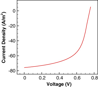
Figure 7. Current–voltage characteristic plot.
Download figure:
Standard imageTable A1. Overview of the parameters used.
| Parameter | Symbol | Numerical value | Units |
|---|---|---|---|
| Electron effective density of states | NC | 2.5 × 1025 | m−3 |
| Hole effective density of states | NV | 2.5 × 1025 | m−3 |
| Electron zero-field mobility | μn | 2.5 × 10⁻⁷ | m2 V−1 s−1 |
| Hole zero-field mobility | μp | 3.0 × 10⁻⁸ | m2 V−1 s−1 |
| Band gap | Eg | 1.34 | eV |
| Photon flux | Γ0 | 4.31 × 10²¹ | m−2 s−1 |
| Donor relative dielectric constant | D |
6.5 | — |
| Acceptor relative dielectric constant | A |
3.9 | — |
| Absorption coefficient | α0 | 2 × 10⁷ | m−1 |
| Average exciton lifetime | τX | 1 × 10⁻⁶ | s |
| Boltzmann constant | kB | 1.3806503 × 10⁻²³ | m2 kg s−2 K−1 |
| Room Temperature | T | 300 | K |
| Elementary charge | q | 1.60217646 × 10⁻¹⁹ | As |
4.2. Idealized 2D morphology
This section analyses the electrical properties of a sawtooth morphology with device dimensions, feature size and interface area identical to the realistic morphology analyzed in the previous section. This provides a means to assess the performance of a realistic heterogeneous polymer solar cell against an idealized morphology.
Figure 8(a) shows a sawtooth morphology with 35 teeth each of donor and acceptor. The device dimensions are maintained same as that of figure 5(a). The number and height of teeth is calculated to get an average feature size of 15 nm and the same interface area. The material parameters and simulation settings are same as that for realistic morphology simulation.

Figure 8. Cross-section of the active layer of an 'idealized' polymer photovoltaic device.
Download figure:
Standard imageThe charge densities (figures 8(c) and (d)) are observed to be maximum at the respective electrodes (anode for holes and cathode for electrons) and decrease toward the opposite electrode. Away from the electrodes, the maximum values of charge density are found near the DA interface. As shown in figure 8(e), maintaining an exciton generation rate distribution similar to realistic morphology case gives an exciton density distribution with maximum values in the donor region lying between the anode and DA interface.
Figure 9(a) shows the x-component of the electric field calculated under short-circuit conditions. This picture is similar to the results presented by Buxton and Clarke [2]. Similar to the realistic morphology case, the y-component (figure 9(b)) of the electric field is an order of magnitude larger than the x-component.
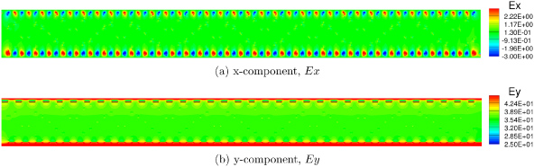
Figure 9. Electric field distribution.
Download figure:
Standard imageThe comparison of current density distribution plots for the realistic morphology (figures 5(f) and (g)) and idealized morphology (figures 8(f) and (g)) clearly reveals the superiority of the sawtooth structure which, unlike the heterogeneous structure, allows all the charges generated at the DA interface to be collected at the electrodes. Additionally, full contact of donor material with anode and acceptor with cathode augments the charge collection process even more. Figure 10 highlights this difference in performance between sawtooth and realistic device structures.

Figure 10. Comparison of the current–voltage plot of realistic and idealized morphologies.
Download figure:
Standard imageIn order to further tune the realistic device morphologies to obtain high short-circuit current densities, we investigate the effect of gradual increase in the feature size while maintaining the same blend volume fraction, on the sub-processes involved in current generation process.
4.3. Effect of interfacial area
In this section, we study the effect of systematically changing the interface area and in turn the feature size of the devices on photovoltaic properties. A similar study delineating the effect of increasing interfacial length on the current density was undertaken by Buxton and Clarke [2]7.
We consider realistic device morphologies as shown in figure 118. for the present analysis. The different morphologies shown in figure 11 show variation in the (a) interfacial area, (b) feature size and (c) electrode contact area (acceptor with cathode and donor with anode) simultaneously. An increase in the interfacial area corresponds to a decrease in feature size. The electrode contact area remains relatively unchanged, as the volume fraction of each material in the blend is same. A large interface area would result in greater opportunity for the excitons to dissociate. However, it also deteriorates the charge transport due to high intertwining of pathways and greater number of isolated islands and dead-ends.
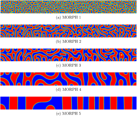
Figure 11. Morphologies with gradual variation in interfacial area.
Download figure:
Standard imageThe material and simulation parameters are identical to the previous section. Figure 12 shows the current–voltage characteristic curves obtained for the morphologies shown in figure 11. This shows that the morphology with highest interfacial area has the best performance suggesting a dominant role played by exciton dissociation rate in deciding the final performance. To further understand the role played by the DA interface, the relative effect of interfacial area on the sub-processes involved in light absorption to charge collection stage (generation, dissociation and relaxation of excitons, charge recombination) is analyzed. Figure 13 shows increasing interfacial area plotted against the integral of
,
 ,
and
,
and
 . The overall exciton generation rate
(figure 13(a)) remains relatively unchanged for different interface areas. This is due to using the same device dimensions and material volume fractions. Figure 13(b) shows a sublinear increase in exciton dissociation rate with increase in interfacial area suggesting a reduced increase in
for any further increase in the interfacial area. A reverse trend is observed for exciton relaxation rate
. The charge recombination
, which limits the device performance, shows an almost linear increase with interface area.
. The overall exciton generation rate
(figure 13(a)) remains relatively unchanged for different interface areas. This is due to using the same device dimensions and material volume fractions. Figure 13(b) shows a sublinear increase in exciton dissociation rate with increase in interfacial area suggesting a reduced increase in
for any further increase in the interfacial area. A reverse trend is observed for exciton relaxation rate
. The charge recombination
, which limits the device performance, shows an almost linear increase with interface area.
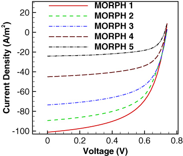
Figure 12. Current–voltage characteristic plot for the morphologies shown in figure 11.
Download figure:
Standard image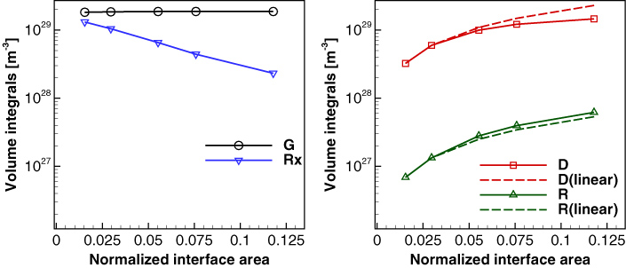
Figure 13. The effect of interface area on the integral of (a) exciton generation rate
, exciton relaxation rate
, and (b) exciton dissociation rate
, charge recombination rate
, over the domain under short-circuit condition. The dashed lines in (b), which represent linear increase, are curved on account of being plotted on a semi-log plot.
Download figure:
Standard imageThe increase is charge recombination rate
is overshadowed by increase in exciton dissociation rate and decrease in exciton relaxation rate
, thereby resulting in a net increase in device performance. The charge recombination increases super-linearly with interface area, whereas the increase in exciton dissociation is sublinear, which would lead to diminishing performance improvements with further increase in interface area.
4.4. Three-dimensional simulation
We showcase the capability of the framework to simulate 3D realistic morphologies with figures 14 and 15. Figure 14(b) shows the morphology of the device used in this study. The calculated electron and hole current densities are shown in figures 14(e) and (h), respectively. The cathode and anode facing views are also included to aid visualization. Figure 15 shows the corresponding morphology and current density plots for ideal morphology. As can be observed from figures 14 and 15, the current density for ideal morphology is much larger than that for real morphology due to better charge transport pathways and electrode contact area (cathode contact area for acceptor and anode contact area for donor).

Figure 14. Electron and hole current distributions for real morphology. Rows 1, 2 and 3 show various views of the microstructure, electron current density and hole current density, respectively.
Download figure:
Standard image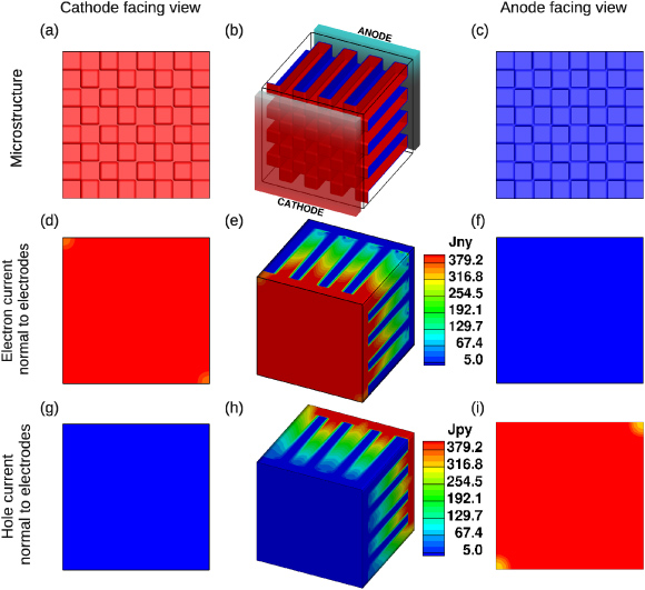
Figure 15. Electron and hole current distributions for ideal morphology. Rows 1, 2 and 3 show various views of the microstructure, electron current density and hole current density, respectively.
Download figure:
Standard imageFor real morphology, some features which appear as isolated 'islands' in two dimensions may have direct pathways to electrode in 3D, and in general, 3D structures may provide more number of pathways from charge generation site to charge collection site than an equivalent 2D device structure. Hence 3D simulation helps visualize and analyze the charge transport properties which are not easily seen to 2D simulations.
5. Conclusions and future work
The ability to correlate morphological features with each stage of the current generation process will be immensely helpful to minimize performance losses. Quantification of morphological effects on performance based on experimental investigation is very time consuming and resource intensive or prohibitively costly in case of a high-throughput study on a range of microstructures. This necessitates development of a computational framework that can be used as a virtual characterization tool for detailed analysis.
We showcase an efficient, dimensionally independent, finite-element-based framework for high-throughput interrogation of realistic percolating microstructures. (1) A parallel implementation of the framework is showcased and results from scalability analysis are shown. (2) The modular structure of the framework enables quick evaluation of various quantities (e.g.
,
, J) over the entire domain. (3) A comparison of a typical percolating and idealized sawtooth type microstructure revealed a short-circuit current gain of more than twice for the latter. (4) We also investigated the effect of feature size on the photovoltaic properties of heterogeneous interpenetrating microstructures. This helped us understand the relative effect of feature sizes on exciton dissociation and charge recombination. The increase in exciton dissociation due to increase in interfacial area tapers off for a feature size of around 10 nm at which point charge recombination starts to play a dominant role.
Future work consists of analyzing the charge transport improvement due to electrode surface engineering [51]. Other avenues of work include predicting 3D optimal morphologies for maximized charge generation and transport.
Acknowledgments
B G and H K K were supported in part by NSF PHY-0941576, NSF CCF-0917202 and NSF CAREER Award. The authors thank Olga Wodo for the images of active layer microstructures and discussions.
Appendix.: Material parameters and universal constants [2, 42, 45, 52, 53]
The typical parameters and universal constants used in the simulations described here are summarized in table A1. The material properties are typical for annealed P3HT:PCBM based devices. The short-circuit current is highly dependent on the values of charge mobilities μn and μp. It also depends on overall exciton generation rate which is in turn dependent on the values of photon flux Γ0, absorption coefficient α0 and exciton lifetime τX. As the boundary condition for electrostatic potential φ is a function of band gap, the open-circuit voltage VOC is in turn highly dependent on band gap Eg.
Footnotes
- 1
This model breaks down under high electric field and when the device dimension (distance between the electrodes) is short compared with the carrier mean-free path (∼5–8 nm for donor material [31]). Carriers accelerate under high electric field, and scattering is not sufficiently strong to bring the carrier temperature back to lattice temperature. A short high-field region causes the distribution function to become highly asymmetric which cannot be approximated by equilibrium distribution function. The typical thickness of the active layer of an OSC device is around 100 nm, which is much larger than the carrier mean-free path. The range of interest for the externally applied potential, in order to characterize the device, is from zero volts to the open-circuit voltage. Thus, the device dimensions and operating conditions for OSC devices permit the use of drift–diffusion model.
- 2
The most promising candidate morphologies from such high-throughput analysis can subsequently be subjected to more rigorous interrogation, thus significantly cutting down on computational overhead.
- 3
The white region denotes Regio-regular poly(3-hexylthiophene) (rrP3HT or polymer) and black region is [6,6]-phenyl-C61 butyric acid methyl ester (PCBM or fullerene).
- 4
Indium tin oxide (ITO) covered with a conducting polymer like poly(3,4-ethylenedioxythiophene): poly(styrenesulfonate) (PEDOT:PSS) and aluminum are examples of transparent anode and reflecting cathode, respectively.
- 5
As the expressions for current densities involve derivatives of the calculated charge densities and potential, large errors may be introduced while post-processing for current density vectors. We have developed an efficient current calculation strategy [36] to calculate current density in the entire domain, based on replacing the charge densities by their quasi-Fermi level counterparts.
- 6
This is usually the case. However, some electron acceptors can also absorb light to generate excitons, e.g. PC71BM [46].
- 7
This seminal work [2] investigated regular sawtooth morphologies with direct pathways for charges to the electrodes. This study extends it to include convoluted morphologies with bottlenecks and cul-de-sacs.
- 8