
Abstract
Dielectric barrier discharges (DBDs) are plasmas generated in configurations with an insulating (dielectric) material between the electrodes which is responsible for a self-pulsing operation. DBDs are a typical example of nonthermal atmospheric or normal pressure gas discharges. Initially used for the generation of ozone, they have opened up many other fields of application. Therefore DBDs are a relevant tool in current plasma technology as well as an object for fundamental studies. Another motivation for further research is the fact that so-called partial discharges in insulated high voltage systems are special types of DBDs. The breakdown processes, the formation of structures, and the role of surface processes are currently under investigation. This review is intended to give an update to the already existing literature on DBDs considering the research and development within the last two decades. The main principles and different modes of discharge generation are summarized. A collection of known as well as special electrode configurations and reactor designs will be presented. This shall demonstrate the different and broad possibilities, but also the similarities and common aspects of devices for different fields of applications explored within the last years. The main part is devoted to the progress on the investigation of different aspects of breakdown and plasma formation with the focus on single filaments or microdischarges. This includes a summary of the current knowledge on the electrical characterization of filamentary DBDs. In particular, the recent new insights on the elementary volume and surface memory mechanisms in these discharges will be discussed. An outlook for the forthcoming challenges on research and development will be given.
Export citation and abstract BibTeX RIS

Original content from this work may be used under the terms of the Creative Commons Attribution 3.0 licence. Any further distribution of this work must maintain attribution to the author(s) and the title of the work, journal citation and DOI.
1. Introduction
Dielectric barrier discharges (DBDs) are self-sustaining electrical discharges in electrode configurations containing an insulating material in the discharge path. This so-called dielectric barrier is responsible for a self-pulsing plasma operation and thus, the formation of a nonthermal plasma at normal pressure. They are also known as 'silent discharges', 'barrier discharges' or 'ozonizer discharges'. The partial gas discharges occurring in insulated high voltage systems can also be considered as DBDs. First introduced for the generation of ozone in 1857 [1], they have opened up many other fields of application, e.g. surface treatment, degradation of pollutant molecules in gases, pumping of gas lasers, plasma displays, and generation of excimer radiation. Since the 1990s they have been explored for the biological decontamination of medical devices, air flows, and tissues. DBDs are also considered as sources for the electric wind in aerodynamic control systems or used in novel analytical detection devices.
Due to their high technological relevance its principle and applications have already been described in detail in comprehensive textbooks and review papers, e.g. [2–6]. This review is intended to update this information by giving an overview on the progress in the field within the last two decades. Therefore, in the first and second part, the main basic configurations and principles of DBDs as well as the spectrum and characteristics of the different discharge regimes will be summarized, respectively. The third part will give a broad overview on DBD reactors and plasma sources for all current fields of application. It will include already known concepts but extent this to new arrangements which were developed for the exploration of new applications, e.g. for treatment of biological samples or liquids. The technical details will not be given as this part aims to demonstrate the different and broad possibilities of DBDs. These can be found in the cited literature. The intention of this part is also to show the similarities and common aspects of devices for the different application areas. The fourth part will be devoted to the progress in the understanding of the discharge physics with the focus is on single filaments as the elementary object of the most common discharge mode of DBDs. Due to the presence of insulating walls a high complexity of plasma-surface interaction and breakdown processes has to be considered. The new insights on the fundamental volume and surface memory mechanisms in these discharges, obtained by new diagnostic approaches, modeling and theory will be summarized. The contribution will conclude with an outlook to future research.
It has to be mentioned that a considerable progress was also obtained on DBD-based plasma chemistry and structure formation. The review will not cover this and the reader is referred to other topical reviews and books, e.g. [2, 4, 5, 7–12].
2. Principles and configurations
2.1. Basic configurations
DBDs configurations and principles are characterized by the presence of an insulating material in the discharge path. Typically, dielectric materials such as glass, quartz, ceramics, enamel, mica, plastics, silicon rubber or teflon are used. To operate a plasma at normal pressure with moderate high voltage amplitudes the discharge gap is typically in the range of 0.1–10 mm. Because of the capacitive character of the discharge arrangement alternating or pulsed high voltage is required. The high voltage amplitude is in the range of 1– . Based on the general description different configurations can be realized. The main basic configurations in planar geometry are sketched in figure 1.

Figure 1. Basic planar configurations of DBDs: (a) volume DBD (1-symmetric, 2-asymmetric, 3-floated dielectric); (b) surface DBD (1-symmetric, 2-asymmetric 'actuator' design); (c) coplanar discharge.
Download figure:
Standard image High-resolution imageIn the volume DBDs one or both electrodes are covered by the dielectric barrier(s) ( and
and  ) or a dielectric layer is separating the gas gap in two sections (
 ) [13]. In configuration (
 ) both metallic electrodes are protected from the reactive species that might be formed in the plasma. In configurations (
 ) one or both metallic electrodes are exposed to the plasma which can lead to its erosion or corrosion, but the plasma can be operated at lower high voltage amplitude than in (
 ) since a larger fraction of the applied voltage drops over the gas gap. Since the total capacity is doubled compared to (
 ), a higher amount of charge per electrode area element can be dissipated. In (
 ) the dielectric is floated. This has no influence on the general operation principle. It is just an option for the treatment of gases by DBDs. In the surface DBDs (
 ) both electrodes are in direct contact with the barrier [14]. Here, the plasma is formed in the gas at the exposed surface electrode and propagates along the dielectric surface while the sheet or counter electrode is embedded in an additional dielectric layer (not shown in the figures). Such configuration has been realized by mesh wire electrodes mounted on an insulating plate with the second sheet electrode below the plate [15], by printing of structured metal films on the insulating plates, or the structured etching of circuit boards [16–18]. The asymmetric configuration (
 ) is well described in the literature on plasma actuators e.g. [19, 20]. In the coplanar discharges (c) both electrodes are embedded in the insulator and the discharge appears in the gas above the dielectric surface [21–24].
2.2. Special configurations
The research and adaptation of DBDs on different problems has lead to several novel configurations. A few examples are given in figure 2.

Figure 2. Special configurations of DBDs: (a) sliding discharge. Reproduced from [19]. © IOP Publishing Ltd. All rights reserved; (b) capillary plasma electrode discharge © (2000) IEEE. Reprinted, with permission, from [26]; (c) microcavity plasma array [27–29]; (d) piezo-electric operated DBD (cross sectional views). Reproduced from [37]. © IOP Publishing Ltd. All rights reserved.
Download figure:
Standard image High-resolution imageThe so-called sliding discharge (figure 2(a)) has been developed for plasma actuation and catalysis [19, 25]. The idea is to enhance the area of plasma-surface interaction by enforcing the plasma to develop along the gas-dielectric interface. The configuration is based on the asymmetric surface DBD. The third electrode (sliding electrode) is biased with an additional potential that accelerates the charge carriers along the interface. Finally, the plasma slides over the surface.
A special form of DBDs is the capillary plasma electrode discharge (figure 2(b)) [26]. The dielectric is perforated which leads to more uniform and higher density plasmas than in classical DBDs (see section 3). A relatively new type of DBDs are the microplasma arrays. They are produced by micro-machining techniques (e.g. anisotropic etching) on silicon layers [27, 28]. The cavities can have a rectangular cross section as shown in figure 2(c) or of an inverted square pyramid. The silicon-electrode is coated with a μm thick film of silicon nitride as the barrier and a nickel array as the second electrode. The use of polymer-based replica molding processes allows fabrication of flexible arrays of microcavity plasma devices. Linear plasmas with trapezoidal or parabolic spot profiles, generated within nanoporous alumina microchannels were studied more recently. Cavity dimensions as small as 3 μm with aspect ratios (length:width) of 1000:1 can now be realized. Microplasmas have attracted considerable attention in various applications, such as mask-less micro-fabrication processes, synthesis of nano-scale particles, in life-science (medicine) as well as meta-materials (wave-propagating media with extraordinary properties) [29, 30].
Beside insulators other barrier materials has been used. In the so-called resistive barrier discharge a highly resistive sheet (e.g. a top-wetted ceramic or silicate layer with a resistivity of a few MΩ cm–1 or higher) is covering one or both electrodes. It acts as a distributed resistive load [31, 32], playing the same role as the dielectric barrier, but it enables plasma operation also by DC high voltage. The current is self-pulsing with a repetition rate of a few kilo-Hertz and pulse durations of a few microseconds. Systems with semiconductor electrodes at cryogenic temperatures were studied, e.g. in [33–35]. In order to control the discharge inception the semiconductor is illuminated externally. The illumination increases the specific conductivity and thus, the capacity per electrode area unit (also called effective capacity). Consequently, the voltage drop across the gas gap increases and leads to electrical breakdown. This research is not only motivated by studying the plasma dynamics but also the development of infrared image converters with high response speed [36].
As mentioned above, DBDs and other atmospheric plasmas sources require high voltages for discharge operation. The reduction of the voltage amplitude is possible by the utilization of piezoelectric crystals. Mechanical, thermal, or electrical forces alter the crystal structure and change the magnitude of its polarization. Thus, the surface potential can be increased to values which allow gaseous breakdown [37–39]. The generation of DBD-based plasma jets by means of piezoelectric transformers has been demonstrated and many applications like lighting and ozone formation are possible [37, 38, 40]. As shown in figure 2(d) the DBD appears between a grounded dielectric covered electrode and the ceramic surface of the piezoelectric crystal. The high surface potential is generated via resonant electrical-mechanical vibrations induced by an AC voltage with low amplitude. Recently, thermally excited pyroelectric crystals were used to generate corona-like discharges [41]. Despite the power of the plasma is limited in these concepts, the compactness and low-voltage driving makes them promising for many industrial applications.
A multitude of atmospheric pressure plasma jets which implement a DBD in the broader sense exist [42–45]. Most of them are coaxial, i.e. the barrier is a tube of dielectric material and thus, forms the gas nozzle (see figures 3(a) and (b)). The gas flowing through the arrangement extends the plasma as an effluent into the surrounding gas. Beside coaxial arrangements planar or linear plasma jets are possible and can treat surfaces with several meters length [46, 47]. As an example, in figure 3(c), a double slit volume DBD with a ribbed grounded electrode and a non-equidistant discharge gap is shown. Two parallel effluents are formed by the gas flow and merge into one [46, 48]. Whether the plasma jets can be considered as classical DBDs or not is mainly determined by the frequency of the applied voltage (see section 3). Since this review is not intended to focus on plasma jets, the reader is referred to recent comprehensive review articles in this field, e.g. [43–45, 49]. Indeed, some of the principles and diagnostic approaches described in the following can be applied to plasma jets, in particular for the characterization of its core plasma inside the nozzle.

Figure 3. DBD-based plasma jet configurations: (a) core plasma generated inside dielectric tube with two metal ring electrodes outside the tube; (b) configuration with one metal electrode outside and a concentric needle electrode inside. Reproduced from [44]. © IOP Publishing Ltd. All rights reserved; (c) double slit linear DBD-based plasma jet. Reproduced from [48]. © IOP Publishing Ltd. All rights reserved,
Download figure:
Standard image High-resolution image3. General operation and discharge regimes
In most studies and applications DBDs are operated with AC high voltage in the kHz-range. Within the last two decades more and more studies have extended this to pulsed or radio-frequency (i.e. frequencies of 1 MHz and more) driven discharges. In any case the DBD arrangement has to be interpreted as a capacitive element. Thus, the displacement current is determined by the total capacity of the DBD arrangement as well as the time derivative of the applied voltage. Indeed, the total capacity is given by the dielectric constant and the thickness of the barrier(s) as well as the geometry of the DBD arrangement.
3.1. The classical operation regime and filamentary plasmas
In case of kHz-operated DBDs (AC or pulsed) the electrical breakdown leads to the charging of the insulator surfaces. The surface charges induce an electric field opposed to the applied electric field. Thus, the total field is decreased and the discharge extincts. The insulator electrically acts like a load which limits the amount of charge and the average current density in the gas. This keeps the plasma in the nonthermal regime, i.e. without such limitation, a spark or arc discharge would be formed. In case of AC high voltage a breakdown occurs during the increase of the value of the applied voltage (i.e twice per high voltage period) and the discharge activity stops, when the voltage maximum is reached. In case of unipolar pulsed operated DBDs the surface charges induce an electric field at the falling slope of the high voltage pulse which causes the second breakdown in the same high voltage period (also referred to as back discharge) [50–53].
At medium, normal and even higher pressures, gas discharges tend to constrict due to the streamer breakdown mechanism [4, 54, 55]. Electron avalanches create a space charge and thus an additional electric field which enhances the growth of secondary electron avalanches locally. Consequently, the ionized region and the perturbation of the electric field grows rapidly and forms distinct plasma channels. Due to the repetitive generation these so-called microdischarges visually appear as thin discharge channels, often named filaments. DBDs in most molecular gases but also in argon or mixtures of noble gases with molecular gases are typical examples of such filamentary plasmas. Filamentary plasma generation was also obtained in radio frequency operated asymmetric surface DBDs [56]. The frequency (13.56 MHz) is high enough to trap electrons in the discharge region across successive cycles. It leads to an increase in the length, intensity and degree of branching of the discharge channels.
The microdischarge channels are spreading on the barrier surface covering a region much larger than the original channel diameter. An increase of the voltage amplitude in a AC operated, plane parallel discharge gap DBD leads to a higher number of microdischarge per active phase, but will not change the amount of charge transferred to a single microdischarge [57–61]. The latter depends—apart from the gas type and pressure—on the design parameters of the DBD. It is proportional to the discharge gap g [62]. In [63, 64] it was shown that the values are independent on electrode material but depend on the width of the discharge gap and the specific capacitance of the barrier ( ). In [65] it scaled with
  while in [66] it scaled roughly with (
 ).
).
The duration of microdischarges is determined by the gas as well as the discharge arrangement (gas gap, type and thickness of barriers). In air at 1 bar and 1 mm discharge gap the microdischarges have a duration of about 10–100 ns with a total transferred charge of 0.1–10 nC. Microdischarges in argon can have a duration of a few μs. Although maximum current density can reach up to 1000 A cm−2 significant gas heating in the remaining channel does not happen because of the short duration.
3.2. Diffuse DBDs
For more than 100 years, DBDs were known to operate only in the filamentary regime. In the 1970s it was shown that external pre-ionisation by UV-photons or x-rays enable the generation of uniform DBDs in gas laser devices [5, 67]. Uniform or diffuse means that the surface cross section is covered by the discharge more or less entirely, although the plasma is not necessarily homogeneous in axial direction. Already in 1969 the first AC operated uniform DBD in helium was described [68]. In the 1990s further investigations of uniform DBDs were presented in reproducible manner and verified [69–75]. They are also known to be generated in plasma display panel cells [72, 76]. In all these examples discharge uniformity is possible without external pre-ionisation but requires specific conditions, in particular on the gas composition or purity. Furthermore, it depends on the frequency of applied voltage and the properties of the external electrical circuit limiting the dissipated power [77–80]. It must be noted that a filamentary DBD can appear to be uniform to the naked eye or slow cameras if the number density of microdischarges per cycle is high [80–84]. There can also be transition regimes, where uniform and filamentary mode exists within the same half period or stagger between the two successive half periods (e.g. [69, 85]. The uniform character can be proved by short exposure time photographs combined with fast discharge current measurements. In case of a filamentary DBD individual and erratic appearing current 'spikes' are observed, while in a diffuse DBD much longer current pulses which are in phase with the applied voltage are obtained. Diffuse DBDs were described either as atmospheric pressure townsend discharge or atmospheric pressure glow discharge (APGD) in the literature (see e.g. [80] and references therein). They have been generated in pure gases (helium, neon, nitrogen) as well as gas mixtures (argon with ammonia, air with precursor molecules) [71, 80, 83, 84, 86].
An APGD is typically observed in rare gases like helium and neon with discharge gaps of a few millimeters [73, 80, 87–89]. These gases are characterized by a relatively high gas ionization at comparatively low electric field strength which can lead to a considerable 'slow down' of the breakdown and avoid the formation of rapid electric field gradients as it is obtained with the streamer mechanism [5, 13, 90, 91]. Furthermore, the metastable states of noble gases are considered to induce a variety of multistage ionization processes. In particular when impurities or admixtures of nitrogen are present in the gas, Penning ionisation (chemi-ionisation,  , with
  representing an excited (in particular metastable) species), stepwise ionisation and charge transfer collisions play an important role in the overall ionisation dynamics [72, 80, 92]. The plasma display cells are a typical example of DBDs operated in so-called Penning gas mixtures (in this case neon/xenon) [76, 93]. An essential feature of the APGD is the formation of a cathode fall [80, 88, 89, 94–97] and the discharge is characterized as a subnormal transient glow discharge with one or several narrow current pulses per half period. The current density per pulse is in the range of 1–100 mA cm–2 and thus, orders of magnitude lower than in a microdischarge [86].
An APTD is typically obtained in nitrogen and noble gases in discharge gaps of about 1 mm [80, 98–100]. It is characterized by an exponential increase of the electron density towards the anode and a low space charge production [80, 101]. The current pulse is significantly longer than in an APGD and the current density is lower (0.01–10 mA cm−2).
3.3. Operation at radio frequency
At frequencies in the MHz-range (radio frequency, RF) the current limitation by the dielectric becomes less effective, the breakdown voltage is decreased [26], the discharge operation changes significantly and impedances must be considered. The charge carriers in the volume do not completely diminish between two subsequent voltage half periods and the mobility of the ions is too small to follow the variation of the applied electric field. Thus, ions are trapped in the gap and do not charge up the barriers. Strictly speaking the discharge is not a DBD as the role of barrier is not to induce the self pulsing character. The discharge operates in steady state and its properties are comparable with RF discharges or capacitively coupled plasmas at low and medium pressure [102–106]. As the discharge sustainment is without secondary emission the main electron production and heating likely happens in the sheath region. This discharge regime is called α-mode (in contrast to γ-mode) [107–110]. The discharge mode has significant effects on the plasma parameters [103]. The role of the dielectric here is mainly the protection of the electrode material from plasma species.
3.4. Capillary jet mode
Special discharge modes are also investigated in the capillary plasma electrodes where perforated dielectric barrier(s) or dielectric capillaries from 0.01 to 1 mm and length-to-diameter ratios of about 10:1 cover one or both electrodes (see figure 2(b)). This arrangement exhibits the so-called 'capillary jet mode', i.e. the capillaries serve as plasma sources producing jets of high intensity plasma under certain operation conditions [111]. These jets emerge to the gas gap and support breakdown in the gap leading to a more uniform and stable plasma. This mode also shows a higher electron density than usual filamentary DBDs.
4. Designs of DBD-based plasma sources
Due to the numerous application areas many different DBD reactor or device designs exist. This section aims to give an overview on the current status of the DBD-based plasma source technology. The following subsections show selected examples for the treatment of gas streams, the generation of light, surface/object treatment, plasma medicine and decontamination, and liquid treatment, respectively. The last subsection gives some remarks about the development of desired high voltage power supplies. This overview makes no claim to be complete. The different concepts and possibilities for the design of plasma sources should be shown and inspire new developments.
4.1. Gas treatment with DBD-reactors
The classical reactors for gas treatment (e.g. ozone generation from oxygen or air, pollutant degradation, synthesis) are cylindrical devices as coaxial electrode arrangement. Tubes of insulating materials are used either as the outer electrode (figure 4(a)) and/or covering the inner electrode (figure 4(b)). The electrode can be a metallic film deposited or pasted on the inner/outer dielectric tube wall as the inner/outer electrode, instead of a solid metal electrode. In laboratory reactors metal meshes are often used, but then parasitic discharges outside the tube must be considered. They can lead to an overestimation of the dissipated power [112]. Large scale reactors, e.g. ozone generators, consists of several DBD tubes mounted in a generator tank. In modern ozone generators the inner electrode is coated with enamel [113]. The electrode arrangement also enables the cooling of the discharge tube. These discharge reactors are still the most robust and reliable DBD sources for gas treatment.

Figure 4. DBD reactors or reactor modules for the treatment of gases (cross sectional sketches): cylindrical or coaxial volume DBD with outer (a) and inner (b) dielectric electrode [5, 112]; (c) packed-bed DBD [112] John Wiley & Sons. © 2004 WILEY-VCH Verlag GmbH & Co. KGaA, Weinheim; (d) stacked volume DBD [119, 120]; (e) stacked surface DBD [120, 124]; (f) open microplasma array type system [29] John Wiley & Sons. © 2006 Institute of Electrical Engineers of Japan.
Download figure:
Standard image High-resolution imageIn packed bed reactors (figure 4(c)) pellets or spheres made of dielectric or ferroelectric material are filling the space between the electrodes. The polarization of the pellet material generates regions with high electrical fields and gas discharge appears in the void spaces between the pellets and on their surfaces [114–117]. The field refraction and enhancement at the pellets depends on their shape, porosity, and the permittivity of the filling material. Porous ceramic foams can also be used instead of pellets beds [118]. The advantage of such reactors is that the filling material can have catalytic properties or can be prepared to have a catalytic surface which increases the efficiency and selectivity of the plasma chemical processes [7, 9, 112]. Therefore, they were mainly investigated for the cleaning and conversion of gases.
The stacked volume DBD reactor (figure 4(d)) consists of a stack of dielectric plates and electrodes at alternating potential. Metal plates as well as metal grids can be used [119, 120] and spacers of dielectric material adjust the desired gap distances (in the mm-range). Such compact and well up-scalable DBD reactors are often used for the treatment of exhaust gases and its deodorization [119, 121–123]. A similar arrangement can be realized based on the surface DBD principle (figure 4(e)). Here, the space between the electrodes can be increased without the need for increasing the voltage amplitude as the discharge is generated only on the dielectric surface. However, in such a case only the gas fraction flowing directly along the electrodes is subjected to the active plasma. With an additional electrode an ionic wind can be expelled from the plasma. These ions are charging and deflecting particulate matter similar as in electrostatic precipitators [124]. These arrangements do not increase the back pressure significantly since the gas flows along the electrodes [125]. They are also more easy to construct and more compact than the cylindrical devices mentioned before. However the extra cooling of the electrodes is not possible and in case of a defect of one of the barriers sheets the repair takes more efforts.
The arrangement in figure 4(f) is based on a two insulator coated metal plates [29, 126–129]. A sandwich of at least two plates with about 200 μm wide holes enable the set-up of a microplasma array which can be penetrated by the gas flow. This concept is even more compact than all other mentioned ones and since both electrodes are embedded in the dielectric the oxidation of metallic electrodes is not limiting the lifetime of reactor modules as in all the previous discussed examples. Disadvantages are the higher back pressure and the short retention time of gas particles in the active plasma region. A setup for the purification of inert gases using a DBD plasma together with a rotating sacrificial electrode is presented in [130]. This approach benefits from the fact that the plasma treatment of metallic substrates under inert gases mainly result in its oxidation due to oxygen impurities. Thus, oxygen impurities could be removed—similar as in gettering processes—by plasma-driven chemisorption on the sacrificial metal electrode. As surface properties change the plasma the electrode is under rotation during operation.
4.2. Light generation with DBDs
The generation of light is based on the formation of plasma in dedicated gas mixtures sealed in silica glass vessels [5, 131, 132]. The gas mixture usually contains a buffer gas (mixture of noble gases) to enable low ignition voltage. Planar light panels (figure 5(a)) and cylindrical lamps (b) have been realized. The vessel glass also serves as the barrier. The outer or front electrodes are metallic wire meshes, perforated metallic films or transparent metallic layers. The rear electrode can be utilized as a mirror. Depending on the application UV or VUV-photons emitted from the plasma are used (excimer lamps for special applications, e.g. curring) or these photons are converted to visible light due to the excitation of phosphors coated on the interior surface of the vessel. Flat light panels can also be constructed with coplanar electrodes (figure 5(c)). Such lamps are manufactured by means of thick film printing [5]. In commercial plasma display panels each cell consists of a microscopic DBD with dimension of about 0.1 mm × 0.1 mm. The VUV radiation of the generated rare gas DBD plasma is used to excite phosphors emitting in red, green or blue, respectively [76]. Microplasma arrays as mentioned above are also considered as novel light sources and on the way of commercialization [28].

Figure 5. DBD modules for the generation of light (cross sectional sketches): (a) sealed planar and (b) cylindrical excimer lamp configurations; (c) coplanar excimer lamp configuration. Reprinted from [132], Copyright (2000), with permission from Elsevier.
Download figure:
Standard image High-resolution image4.3. Surface treatment
The most important DBD application in surface treatment today is the activation of plastic foils in order to increase its surface energy prior to bonding, printing, coating, adhesion, or, for cleaning it from organic compounds. The deposition or functionalisation of surfaces is also possible. The scheme of a typical DBD treatment of fabric material, e.g. foils, wool or textiles, is shown in figure 6(a). The material is rolled off and up from storage coils and thus, the surface to be treated is continuously moved through the DBD [2, 5, 133, 134]. It is formed between a dielectric covered electrode (mostly water-cooled) and the surface which is transported over a metallic roll. The rotating drum can also be covered with a dielectric layer. Speeds of up to 10 m s–1 are reached and large facilities can handle plastic webs of 10 m width or more [2, 5, 133].

Figure 6. Schemes for DBD-based surface or object treatment: (a) fabric material treatment [5] (2003) (© Plenum Publishing Corporation 2003). With permission of Springer; (b) cascaded DBD [135] (2004) (© Plenum Publishing Corporation 2004). With permission of Springer; (c) coplanar DBD arrangement (DCSBD) for fabric materials. Reproduced from [22]. © IOP Publishing Ltd. All rights reserved; (d) microplasma stamp [136] John Wiley & Sons. © 2009 WILEY-VCH Verlag GmbH & Co. KGaA, Weinheim; (e) in-package DBD treatment [139] John Wiley & Sons. © 2007 WILEY-VCH Verlag GmbH & Co. KGaA, Weinheim; (f) contacted plasma. De Gruyter [141], Walter De Gruyter GmbH Berlin Boston, [2010]. Copyright and all rights reserved. Material from this publication has been used with the permission of Walter De Gruyter GmbH.
Download figure:
Standard image High-resolution imageThe cascaded DBD shown in figure 6(b) combines the treatment of surfaces and goods by plasma-generated (V)UV radiation and reactive species in one device. It was developed for the biological decontamination of packagings [135]. The discharge consists of a high voltage powered electrode, a sealed glass chamber filled with excimer-forming gas for efficient UV emission, an air flushed gas gap for the generation of the reactive species, and the grounded electrode below the object.
Another principle for the treatment of web and fabrics is based on the so-called diffuse coplanar surface barrier discharge (see figure 6(c)) [22]. It generates a visually diffuse plasma with a high power density in the immediate vicinity of the textile surface. This arrangement allows more uniform plasma treatment without pinholing or other critical changes in the tensile strength of the fabrics.
The microplasma stamps schematically shown in figure 6(d) enable an area-selective treatment of surfaces [136–138]. Therefore, the dielectric is patterned in order to form cavities with a size in the range of 100–500 μm when the stamp is pressed against the substrate. Since the plasma is only ignited in the voids a lateral microstructuring and surface treatment is achieved in a single process step.
A new possibility for the treatment of packed goods is the local application of a surface DBD. The electrode arrangement is contained in a label bonded inside the airtight flexible or rigid package (so-called 'plasma label') as demonstrated in figure 6(e) [139, 140]. The arrangement sketched in figure 6(f) is an example for a DBD device which can be designed as a hand-held device. It allows to bring the plasma in closed proximity to the surface. The process is supported by a gas flow through the arrangement but the substrate is not integrated ('contacted plasma') [141, 142]. The gas flow allows the reduction of operating high voltage amplitude if noble gases are used and can influence the compostion of the plasma, similar as in plasma jets. It is probably an interesting device for the treatment of curved objects.
DBDs are also considered for the enhancement of other material processes. Novel hybrid laser-plasma methods were presented in [143, 144]. The method combines an laser with DBD-based plasma jet for the chemical reduction of glass surfaces or micro-structuring purposes. The combination reduces the ablation threshold and improves the machining quality. Furthermore, the DBD was found to act as a thermal lens for the the laser beam causing a defocussing by several millimeters [144].
4.4. DBDs for plasma medicine and decontamination
Many activities in the exploration of plasma life-science applications have inspired new DBD-based plasma sources. The first activities were devoted to the biological decontamination of surfaces, medical devices and other sensitive goods [145, 146]. The cascaded DBD, the in-package surface DBD and the contacted plasma device discussed in the previous subsection has also been mainly considered for such applications [147]. A commercial device for the cleaning and sterilization of liquid transfer devices such as pipette tips, cannulae and pin tools is available [148]. In [149] a DBD for the decontamination of rotating cutting tools is presented. The metallic cutting tool acts as grounded electrode and two equal dielectric isolated electrodes realize the plasma treatment from both sides. The in-package treatment and decontamination of food can also be realized in a large-gap volume DBD in air with up to 4 cm discharge gap. High voltage amplitude between 50 and 70  is required under such conditions [150].
The usage of plasmas in therapeutic applications requires plasma sources which are flexible to use (e.g. as a handheld device) as well as safe for patients and doctors [151, 152]. One of the first DBD devices used for the treatment of animals and humans is the floating electrode DBDs shown in figure 7(a) [153–157]. The treated object itself serves as the grounded electrode. The discharge device consists of a dielectric-protected powered electrode and is operated by high voltage pulses. The plasma is in direct contact with the treated surface. The electrical shock is avoided due to the limited current of the DBD. Decontamination of skin, coagulation of blood and other biological effects have been demonstrated with such sources. There are also commercial devices available and already used in clinical trials [158, 159].

Figure 7. Schemes of DBD sources for plasma medical applications (a) floated electrode volume DBD [153] (2006) (© Springer Science+Business Media, Inc. 2006). With permission of Springer; (b) polymer film-based surface DBD. Reproduced from [160]. © IOP Publishing Ltd. All rights reserved; (c) fabric-based surface DBD [142, 164].
Download figure:
Standard image High-resolution imageNew developments use flexible materials or arrays of movable electrodes. Such principles allow the treatment of objects with a complex geometry as extremities or other bodily parts [142, 160–163]. All these devices are usually operated with classical AC high voltage in the range of several kHz. The example shown in figure 7(b) is made of a printed circuit board [160]. The dielectric barrier is a polymer film equipped with a thin, uniform powered electrode on one side and a thin, meshed grounded electrode on the other side. The technology enables the construction of formats as much large as required by the wound or skin area to be treated. The advantage of such device is that no current is flowing through the treated sample which increases the electrical safety. The flexible surface DBD plasma strip is able to quickly inactivate significant numbers of bacteria on and in skin. Another example for such kind of flexible DBD is the use of insulated conductor wires in a woven arrangement (fabric-type electrode), as shown in figure 7(c) [142, 164]. Such arrangements can even be constructed as a sticking plaster device. Fabric-based discharge devices could be produced with reasonable efforts and cost as required for one-way instruments in medicine.
Other developments of DBD based plasma sources are dedicated for the inner treatment of long flexible tubes, as found in complex medical devices like endoscopes. Among DBDs with an outer and an inner-tube electrode or the usage of afterglow plasmas [165–167] a bifilar helix electrode configuration enables plasma operation in tubes with length of several meters and an inner diameter of 2 mm [168]. The powered and grounded wire electrodes are equidistantly twisted around the tube. The electrodes are embedded in an additional dielectric layer to avoid discharges outside the tube.
4.5. Treatment of liquids
An increasing number of research on the treatment of liquids has been done. Some DBD-based concepts for the treatment of liquids by DBDs are schematically shown in figure 8. They offer low power density plasma generation compared to pulsed corona discharges. Figure 8(a) shows a surface DBD device for the indirect treatment of water, i.e. the liquid is in vicinity to the plasma and the liquid is not an active part of the discharge generation. Although there is no direct impact this arrangement leads to significant effects, e.g. acidification, or formation of reactive nitrogen and oxygen species. Such studies are important for the understanding of plasma-cell interaction [169] and offers a wide range of applications such as degradation of pollutants and microorganisms in water, the analysis of trace compounds in solutions, or the synthesis of active liquids, species or nano-materials.

Figure 8. Schemes for DBD-based treatment of liquids: (a) indirect treatment by means of surface barrier discharge [169] John Wiley & Sons. © 2010 WILEY-VCH Verlag GmbH & Co. KGaA, Weinheim; (b) direct treatment, i.e. liquid serving as one electrode. Reproduced from [174]. © IOP Publishing Ltd. All rights reserved; (c) water falling film reactor. Reprinted from [175], Copyright (2004), with permission from Elsevier; (d) rotating drum reactor [179] John Wiley & Sons. © 2011 WILEY-VCH Verlag GmbH & Co. KGaA, Weinheim; (e) liquid electrode DBD. Reproduced from [181] with permission of The Royal Society of Chemistry.
Download figure:
Standard image High-resolution imageMany liquids are conductive and can be used as an active electrode for the plasma generation (e.g. [170–174]). Examples for DBDs are shown in figures 8(b)–(d). The liquid is covering the grounded electrode to avoid its charging. Liquid electrodes can also be utilized for the treatment of outer and inner surfaces of tubes and other hollow dielectric bodies as demonstrated in [172].
The water falling film reactor, shown in figure 8(c), consists of a sealed cylinder of dielectric with a concentric hollow metal tube electrode inside and a metal electrode outside [175]. Water or other liquids are pumped through the inner tube electrode and form a laminar flowing layer along the inner metallic tube. This reactor has been demonstrated to be capable of decomposing pollutants in the liquid phase [176, 177] as well as for gas cleaning [123, 178]. A similar concept is realized in the rotating drum reactor (figure 8(d)). A homogeneous, thin film (10 μm, the thickness depends on rotational speed) of bacterial suspension is produced on the rotatable hollow cylinder made of metal and treated by the plasma. Plasma-specific stress responses of bacteria to argon and air plasmas were studied in this set-up [179, 180]. The DBD-liquid electrode setup in figure 8(e) was developed for aqueous analysis with low sample volumes [181, 182]. The analyte is supplied in a dielectric capillary covered with metal layers serving as high voltage electrode. The grounded electrode is a metal wire connected over a high ohmic resistance. The concept has been demonstrated for emission based analysis of liquid solutions and is supposed to be combined with micro-separation devices in the future.
4.6. Power supplies
Along with the improvement of industrial DBD installations and the development of new discharge geometry concepts there has been a significant progress in the field of high voltage power supplies. AC high voltage power supplies, in particular sinusoidal, are still the most common in industry. State-of-the-art in surface processing is the use of variable-frequency drives in connection with high voltage transformers. Modern power supplies of surface treatment stations are microcomputer-controlled and automatically adjust its operation frequency to the resonance point of the system (i.e. capacitance of electrode configuration and inductance of high voltage transformer). The effective ability to control power transfers by means of current magnitude and frequency is highlighted in [183]. Special power supplies have been developed to generate repetitive pulse trains, resulting in an improved distribution of the energy, e.g. [184].
A new trend are solid-state devices that can eliminate bulky high-voltage transformers or realize resonant power supply system topologies for higher energetic efficiencies [5, 185]. Pulsed power supplies and topologies enabling a variety of pulse waveforms (unipolar, bipolar) has been investigated and developed, in particular for ozone synthesis and lighting. A classification of novel and state-of-the-art power electronic pulse inverter topologies for driving DBD-based lamps can be found in [186]. The novel topologies are based on pure resonant operation or a combination of resonant operation and inductor pre-charge. Silicon carbide power semiconductors were implemented in transformer-less topologies and increased the electrical power efficiency of excimer lamps significantly. The piezo-transformer based DBD sources have already been mentioned in the section 2.2.
5. Discharge development in filamentary DBDs
5.1. Methods and techniques
The diagnostics and modeling of DBDs and other plasmas at elevated pressures made a significant progress within the last twenty years. This was possible by the technical developments and the increase of computational power, but has been motivated by the growing technological interest on atmospheric pressure plasmas in general.
The diagnostics of DBDs was for a long time dominated by electrical measurements, optical emission spectroscopy and chemical analysis. In the meantime methods for the spatio-temporally resolved study of the discharge development, laser diagnostics for the determination of active species densities and for the quantitative measurement of surface charges are available. Basic plasma parameters (reduced electric field strength, electron density) has been determined by emission based methods and densities of metastable states have been measured by laser induced fluorescence. Reviews on the methods for the investigation of microdischarges and microplasmas are given elsewhere [187–190] and recently optical diagnostics on atmospheric pressure plasmas are reviewed in [49, 191, 192]. The time resolution and high sensitivity of laser induced fluorescence, two-photon absorption laser-induced fluorescence or broad-band absorption spectroscopy allows the study of the development of key species like metastable molecules, nitrogen atoms or radicals (e.g. OH) [188, 193–197]. Molecular beam mass spectrometry enables the in situ detection of negative and positive ions from DBDs and the study of the ionic chemistry. In case of water vapor admixture or impurities cluster ions are measured [198, 199].
A special approach is the investigation of single filament discharges. The overall yield of plasma processes in DBDs is determined by the multitude of discharges, but the properties of the single discharges determine the main processes. Thus, the rate coefficients of excitation and ionisation processes as well as plasma chemistry depend on the basic parameters in the microdischarge [14, 200]. The investigation of single filaments is possible in special electrode arrangements. Two semi-spherical electrodes (symmetric and asymmetric volume DBDs) [201–206], pin-to-plate electrode configurations (asymmetric volume DBD and surface DBD) [207–209] or two pins embedded in an isolator (coplanar DBD) [210–213] enable sufficient localization and stabilization for dedicated studies.
The short duration of the microdischarges makes current measurements challenging. Current pulses of single microdischarges are measured by well-shielded and fast current probes (Rogowski coils) [62, 214] or via the voltage drop across a non-inductive shunt resistor inserted between the grounded electrode and grounding lead [213] on the special DBD arrangements mentioned above.
The spatial resolution of imaging and spectroscopic methods could be increased up to 10 μm and a technical time resolution of about 12 ps is reached today [215]. State-of-the-art streak cameras reach sufficient time resolution of up to 50 ps and can also analyze erratically appearing microdischarges [215–217]. A considerable progress was also achieved in the analysis of cathode directed streamers in corona and surface discharges [218–222].
The behavior and amount of charge carrier on the dielectric barriers can be investigated by the electro-optic Pockels-effect [223–229]. A crystal serves as the barrier or is directly attached to the discharge channel. The crystal changes its polarization properties with the electric field applied, which is changed by the accumulated surface charges. The first applications of this principle were devoted to the study of dynamics and formation of discharge pattern [229–231] but are now also applied to measure the surface charge during the breakdown. Therefore, the Pockels-method was extended for phase-resolved and thus time resolved studies [232] and the time-resolution was significantly improved to 200 ns [233]. This method has been directly combined with electrical characterization and LIF diagnostics for an identical discharge arrangement in [195, 232, 234, 235]. Another approach for the measurement of surface charges is the fit of discharge delay time from electrical measurements [105]. It is only applicable for very stable discharges.
It must be noted that some electro-optic crystals have distinct differences from the classical dielectric barrier materials. The dielectric constant is considerable higher, the secondary electron emission coefficient is assumed to be smaller than for glass [98, 236], and photo-induced transport of charges on the minutes-scale has been obtained for bismuth silicon oxide crystals [98, 215, 237].
Accompanying the progress on the experimental studies there is an increasing number of publications on the modeling of DBDs and other plasmas at normal pressure, in particular corona discharges and plasma jets. These models calculate the temporal behavior of the electric field distribution in the discharge gap coupled with the dynamics of the charged particles. Different kinds of modeling approaches have been reported, including fluid models, Monte Carlo simulations and particle-in-cell models. A combination of several models is referred to as hybrid models. Comprehensive overviews can be found, e.g. in [238–240]. At normal pressures, the energy gained by the electrons from the electric field will be more or less balanced by the energy lost due to collisions. Thus, the calculation of the average electron energy with an energy balance equation in the fluid model is considered as a reasonable approach [241]. In particular, microscopic fluid models are able to describe the rapid dynamics and behavior of streamers [242–249]. Many of these contributions are not only relevant for plasma technology but also related to the understanding of lightning and transient luminous events in the upper-atmosphere.
In the fluid models the continuity equations for all considered species coupled with the Poisson equation are solved numerically [5, 14, 63, 64, 76, 239, 250–252]. In general the models also incorporate the plasma chemistry, with respective necessary complexity. Rather extensive reaction systems including free radical reactions with more than 1000 elementary reactions have been investigated. Most of the models are one-dimensional (1D, i.e. resolving along the discharge gap axis) but there are also 2D and even 3D simulations [14, 252–254]. Normally the local mean energy approximation is used. Thus, all electron transport parameters and rate coefficients can be described as a sole function of the mean electron energy. The electron energy distribution function is calculated by solving the stationary Boltzmann equation for prescribed electric field strength [255]. Full kinetic models provide the electron energy distribution function as a function of space and time. Spatially 1D simulations are indeed suitable for the analysis of diffuse DBDs. It has also been used for the analysis of single microdischarges [256–258]. It is justified if the discharge inherent time scales are much shorter than the residence time of a unit gas volume in the active plasma zone. In these models the electron energy balance equation is solved to determine its mean energy.
A new input in these activities are studies describing the plasma-surface interaction. First approaches to model the surface electrons were via phenomenological rate equations characterized by sticking coefficients, residence times, and recombination coefficients [259]. Other models consider very complex surfaces as plasma boundaries, e.g. liquid layers [260] or catalysts [261]. A new approach is the theoretical study of the microphysics of plasma-surface interaction [262]. The aim is that the plasma walls are not treated as perfect absorbers for electrons and ions but to describe the charge transfer across the interface by an electron surface layer approach. It considers the accumulation, distribution and release of surface electrons from the surface using a quantum-mechanical surface physics approach. Electron impinging on a solid surface is either reflected, inelastically scattered, or temporarily deposited to the surface. Possible trapping states or sites depend on their energy, the inelastic coupling to the elementary excitations of the surface driving energy relaxation, and the electron affinity of the material. The electron affinity is the energy gap between the vacuum energy and the lower border of the conduction band and thus, it is related to the work function of the material. The properties of the trapping sites of electrons determine their corresponding residence times and penetration depths. For simplicity a floating wall exposed to a quasi-stationary plasma is assumed in the electron surface layer approach, i.e. complications due to the presence of individual discharge channels are not considered, yet. Up to now surface electron sticking coefficients and desorption times were calculated for various uncharged dielectrics [263–265] and the distribution of the wall charge across the interface between a plasma and a floating dielectric surface was determined [266]. Furthermore, the release of electrons from the dielectric surfaces via de-excitation of metastable molecules was investigated [267, 268]. Recently, the absorption of electrons by dielectric walls with positive electron affinity (e.g. alumina, glass) smaller than the band gap was studied and energy-dependent sticking probabilities were calculated [269]. These investigations will provide a deeper insight on the discharge physics at insulating surfaces and the calculation of basic parameters describing the plasma-surface interaction.
All these activities, but also dedicated studies on other atmospheric pressure plasmas (corona discharges, plasma jets) increased the knowledge on the physics of filamentary and diffuse DBDs significantly. In the following subsections only some aspects will be emphasized further, namely the electrical description, the physics of single filaments or microdischarges and the mechanisms determining distinct DBD regimes.
5.2. Electrical behavior and characterization
For many purposes it is sufficient to characterize DBDs by overall electrical quantities, such as the frequency and amplitude of the applied voltage, an average discharge voltage, and the dissipated plasma energy or power. Besides the control of the discharge, these measures are for example useful for the determination of discharge modes. This approach was introduced in 1943 by Manley for ozone generators and is still well accepted in research and technology [270–272]. However, it is not considering the processes at the insulator surfaces or the non-uniform breakdown. It has to be interpreted as a purely macroscopic characterization which is limited in many situations, e.g. when the density of filaments per period is low. Recent activities were addressed to extend this approach in order to include the elementary processes of discharge physics. The topic thus has been developed from a purely macroscopic characterization to an approach that can even be used to characterize single filaments [273] or structured discharge regimes [48, 232].
The simplest electrical approach of a DBD is the lumped-element equivalent electric circuit as shown in figure 9(b) [86, 274–276]. In the non-ignited case the equivalent circuit is purely capacitive and consists of two capacitances, one is resembling the barrier Cd and the other is the gas gap Cg (A in the equations (1) and (2) is the area of the electrode). Both together in linear arrangement form a total capacitance Ccell. The sum of the voltages across the gas gap Ug and the barrier Ud equals to the applied voltage V(t). The voltage Ug is too low to cause discharge ignition as long as the amplitude of the applied voltage is below a certain threshold Vmin and the current i is only the capacitive displacement current icap through the arrangement (amplitude:  ).
).


Figure 9. The classical electrical characterization on a asymmetric, one-sided volume DBD configuration (a) with the most simplest equivalent circuit (b), the schematic development of applied voltage V(t), gap voltage Ug, burning voltage Ub, mean current i and its capacitive component icap (c) and the corresponding voltage-charge plot (d). The circled (i) and (t) stands for 'inception' and 'termination'.
Download figure:
Standard image High-resolution imageThe inception of the discharge is obtained when the applied voltage magnitude V0 exceeds the threshold Vmin at which the instantaneous gap voltage reaches a certain threshold, the burning or discharge voltage Ub. It is a macroscopic parameter which is determined by the gas composition, its pressure and the discharge gap (comp. Paschen law) and it enables the determination of the spatially and temporally averaged reduced electric field strength. Figure 9(c) schematically shows the voltage and current in an AC operated DBD when the discharge is ignited. An additional current is obtained in the active phases between inception ('i') and termination ('t'). In these phases Cg is bypassed and charge is transfered into the gap. This is described by the parallel connection of a variable resistor RP(t) and gas gap capacitor Cg in the equivalent circuit. The equations for the plasma current iP(t), the gap voltage Ug(t) and the total charge Q(t) are as follows.


QP is the charge which is transferred conductively during the discharge ( ). The variable resistor RP(t) can also be symbolized by a variable current source which would make no difference on the considerations about uniform DBDs as discussed in [271, 277, 278]. In this classical approach Ug is considered to be almost constant during the active phase with
  (also shown in figure 9(c)). However, this is not entirely the case for pulsed operated DBDs. Here the applied voltage changes on the typical timescale of discharge inception and thus, the gas gap voltage is not constant during the active discharge [279]. However, the equivalent circuit in figure 9(b) covers this aspect as well as the change of effective capacitance (capacity divided by area) in case of non-uniform discharging (see below). It has to be mentioned that the current slope shown in figure 9 (c) does not resemble the measured curve in a filamentary DBD with a limited number of discharge events which is obtained when the voltage amplitude V0 is just slightly exceeding Vmin. The discharge current then persists of individual peaks and the analysis is more complicated but can also give information about the individual events [57].
The investigation of voltage-versus-charge (V–Q) plots is an established approach since the charge measurement do not require high bandwidth probes and oscilloscopes, in contrast to the recording of current waveforms [272]. A measuring capacitor CM is inserted between the grounded electrode and grounding lead and records the overall charge. The value of CM must be chosen to be significantly larger than Ccell (as a rule of thumb a factor 1000). In case of sinusoidal high voltage the V–Q plot is a straight line with slope Ccell when the discharge is not ignited (and if there are no phase errors on the high voltage probe) [272]. When the plasma is ignited and if Ug is constant during each active discharge phase the V–Q plot is a parallelogram, as schematically depicted in figure 9(d). The four sides represent the different phases during one high voltage period  (frep is the frequency). The parameters Ccell, Cd, Vmin and Ub as well as the total plasma energy per high voltage cycle Eel and total power
  can be extracted directly from the parallelogram [50, 52, 53, 214, 272, 275]. Recently, measurements of Eel were discussed in the context with thermodynamic measurements (performed by fiber-optic thermometers) and calorimetric investigations [280]. Fair agreement between both methods was archived. Energy per cycle or power can be related to the volume of the plasma or the gas flow resulting in specific energies or power densities. To give the values of such similarity measures should become a standard in publications since they enable a reliable comparison of different DBDs and plasma processes.
However, a large variety of V–Q plots, also referred to as Lissajous-figures, diverging from parallelograms is reported in the literature. Round edges at the discharge termination points indicate parasitic resistances Rpar which can occur when the barrier material is heated and thus, becomes conductive. In such cases the V–Q plot can even be deformed to an ellipse and its enclosed area is not necessarily a measure for the dissipated plasma energy [280]. In case of pulsed operated DBDs, asymmetric discharge arrangements, or, unstable high voltage power supplies the shape of the V–Q plot can also differ significantly from a parallelogram (Ug not constant) and one needs to analyze the obtained plots very carefully. If the filaments are ignited in an organized regime (pulsing action or simultaneously ignited groups of microdischarges) the slopes corresponding to the plasma phase are stair-like [272, 281]. To obtain internal discharge parameters such as the discharge current, Ub, and instantaneous power P(t) and energy E(t) in these situations requires the exact knowledge of the capacities Ccell and Cd. These values are then not necessarily determined from the slopes and its calculation is not straightforward. The overall capacity Ccell can be determined from the comparison of the measured current with  when the discharge device is not ignited. The slope of
  points (obtained from a passel of V–Q plots measured at several voltage amplitudes) can be used to determine Cd [279]. The influence of experimental errors of the values for Ccell and Cd was discussed in detail in [282] in particular for pulsed operated DBDs.
In real DBD devices stray capacitances CStray are caused by surrounding capacitances (e.g. cables, edge effects, high voltage throughputs). The resistivity of the secondary side of the high voltage power supply (e.g. transformer series resistance) RS and the parallel losses of energy due to the barrier material and reactor construction (symbolized by resistivity Rpar) can significantly influence the current and charge that are to be measured [283]. Figure 10(b) shows how these parasitic elements can be implemented in the equivalent circuit. The technique of impedance characterization utilized in [186] also allows the quantification of parasitic electrical elements of DBD lamps and its circuits.

Figure 10. Advanced equivalent circuits for DBDs: (a) circuit including stray or parasitic elements; (b) partial discharged volume DBD. Reproduced from [48]. © IOP Publishing Ltd. All rights reserved; (c) surface DBD actuator [288]; (b) and (c) can also be affected by external elements (see outside the dashed box in part (a)).
Download figure:
Standard image High-resolution imageThere has been many studies on the construction of equivalent circuit for DBDs. For example, a circuit for characterization of diffuse DBDs presented in [77] incorporates Zener diodes in order to model the Townsend breakdown and an additional capacitance is introduced to describe the memory effect from one half period to the following. This capacity represents the space-charge cloud formed by charge carrier separation during plasma generation in pulsed operated DBDs [186, 284, 285].
Multiple microdischarges can penetrate the entire discharge area cross section in case of high overvoltages, i.e.  and in plane-parallel discharge arrangements with minor electrode edge effects [279, 286]. In case of DBD arrangements with a low number of microdischarges per half period the individual discharge events correspond with distinct steps in the '
 ' of the parallelogram in figure 9(d) [58, 287]. The mean slopes of this line are then depending on V0 which is attributed to the partial discharging. The modified equivalent circuit in figure 10(b) considers this by splitting the capacitances Cd and Cg into two sections in order to describe a non-discharging areal fraction α and a discharging areal fraction β (only this part has to implement RP(t)) [48]. The slope of the
  t-lines (also called effective or apparent dielectric capacitance) is then smaller or equal to Cd. Its value saturates to Cd with sufficient increase of V0 in a plane-parallel arrangement [286]. In case of the ribbed design of one electrode as shown in figure 3(c) a sharp increase of the effective dielectric capacitance with the voltage amplitude is obtained [48] which can be described as a linear combination of Ccell and Cd. This analysis finally leads to the conclusion that the effect of partial coverage of the dielectric by spreading surface charges is analogous to implementing Cstray in the circuit which significantly affects the determination of Ub, the net charge density across the gap during discharging or the resistivity of the plasma averaged over the discharge area [48].
Surface and coplanar DBDs require even more complicated equivalent circuits which were mostly developed for plasma actuators. A typical example is given in figure 10(c). The edges at point 'i' of V–Q-plots are often not sharp as in figure 9(d) which indicates a non-equal voltage threshold in non-plane discharge gaps or surface DBDs [288]. In surface DBDs the exposed surface of the barrier acts as a third, virtual electrode as it collects charge. Therefore, three barrier capacitances Cd1, Cd2, Cd3 and two gas gap capacitances Cg1 and Cg2 must be considered. The capacitor Cg1 represents the capacitance between the exposed physical electrode (compare with figure 1(b)) and the virtual electrode. The capacitor Cd1 represents the capacitance between the virtual electrode and the encapsulated or covered physical electrode. These capacitors are variable with V0 since the area covered by plasma is not constant. This could be confirmed by studies on surface DBD reactors where the total capacitance of the plasma reactor increases when the operating high voltage amplitude is increasing [289]. The capacitor Cd3 is constant as it is describing the constant capacity due to the direct electric field between the physical electrodes. It induces an additional displacement current but does not affect the discharge itself, i.e. the effect is similar as that of Cstray [288, 290]. Another approach to describe the filamentary, non-regular character of DBDs is the parallel distribution of a certain number of serial connections of finite gas gap and dielectric barrier capacitances [291].
5.3. Single filaments in volume and on surfaces
In air and other DBDs containing nitrogen gas the emission is dominated by molecular bands of nitrogen, namely the second positive system of molecular nitrogen and the first negative system of molecular nitrogen ions. The spatio-temporally resolved development of filaments in a sinusoidal voltage operated volume DBD generated between two semi-spherical electrodes in synthetic air is shown in figure 11. An overview spectrum is shown at the right bottom part of the figure and the investigated spectral ranges are marked. The band heads of the vibrational 0–0 transitions of the second positive system of nitrogen at  = 337.1 nm and of the first negative system at
  nm are investigated. The method used to obtain the temporal development is cross-correlation spectroscopy, the most sensitive method for the investigation of irregular appearing microdischarges [201, 203]. The discussed results have also been used to calculate the axially and radially resolved evolution of the reduced electric field strength E/N [292].

Figure 11. Evolution of light-intensity distributions for 0–0 vibrational transition of the second positive system ( = 337.1 nm) and the first negative system (
 = 391.4 nm) of nitrogen (see emission spectrum for spectral range λ = 290... 450 nm) of microdischarges in AC-operated volume DBD in synthetic air at atmospheric pressure (discharge gap 0.9 mm; voltage amplitude of 12
  frequency of 6.9 kHz; accumulation over about 109 microdischarges in total). © (2008) IEEE. Reprinted, with permission, from [294].
Download figure:
Standard image High-resolution imageFor each transition the observed spatio-temporal distributions of the microdischarge luminosities are determined by the population of the upper electronic states via direct electron excitation and collisional quenching. The excitation rates are directly proportional to the electron density and the rate coefficients [293]. According to the corresponding excitation energies (11 eV versus 18.7 eV) the signal at  represents the development of E/N, while the signal at
  can be attributed as a convolution of the electric field and the electron density. From the results in figure 11 the microdischarge development can be described as follows.
(1) The (Townsend) pre-phase is characterized by a weak, localized light spot at the anode (see figure 11( , a)). It is caused by a slight distortion of the electric field due to charge accumulation in front of the anode by means of electron avalanches. This phase can last for several 100 ns [201, 204].
(2) The propagation phase of a cathode-directed ionisation wave (positive streamer mechanism) starts when the local electric field strength of the accumulated positive space charge reaches a critical value. As shown in figures 11(b)–(f) it transits the 1 mm long discharge gap within about 2 ns.
(3) The two local maxima in figures 11(g) and (h) of  (left series of pictures) correspond to two active zones of the microdischarge with different properties [201]. The anode glow is caused by electrons drifting and accelerated behind the ionizing wave towards the anode. Near the cathode, a high electric field is formed. Due to charge accumulation on the dielectric surfaces, considerable broadening of the microdischarge channel, branching, and expansion on the insulator surfaces is obtained.
(4) The decay phase is initiated by the accumulation of charge carriers on the barrier surfaces. The axial electric field is reduced within about 10 ns (figures 11(h) and (i)) and the plasma current drops down. Charge carriers and long lived excited species from the discharge channel can remain in the discharge gap. Ions are drifting to the electrodes on timescales of 1 μs, the most important chemical reactions occur on the micro- to millisecond time scale [2, 4, 200].
The anode glow phase can show an even more complex behavior. A striated or stratified structure as known from low and medium pressure glow discharges has been investigated for single microdischarges in argon at atmospheric pressure under certain conditions [295, 296].
The analysis of the single filament volume DBD in synthetic or dry air along the microdischarge axis (without radial resolution) for asymmetrical discharge configurations [204] and for a coplanar DBD arrangements [210, 211] have shown qualitatively the same mechanism of electrical breakdown and discharge development, but the experimental findings reveal that residual surface charges on the dielectric covered electrode cause local enhancement of the electric field in the pre-phase and promote the emission of electrons. This is in agreement with simulations [252, 297].
The decay phase of the microdischarge development is determined by the properties of the anode. The accumulation of negative charge on the surface of the dielectric covered anode results in a faster decrease of the electric field strength within the discharge channel as for the case when the anode is metallic. Above the cathode surface a long-lasting (up to 150 ns) and about 30 μm thin layer of enhanced electric field strength is observed. These values correspond to simulation results describing the cathode layer on a metal cathode in asymmetric volume DBDs [63, 64].
The pulsed operation with rectangular high voltage pulse with a gradient of about 250 V ns–1 of a similar single filament volume DBD as discussed above revealed a comparable discharge development as in sinusoidal operated DBDs. But, due to the three orders of magnitude higher voltage steepness in case of the pulsed DBD, the pre-phase is limited by the pulse rise time. Thus, less space charge can accumulate before the breakdown. This leads to a shorter pre-phase but to an increase of the burning voltage and, consequently, to a larger amount of transferred charge and a higher amount of dissipated energy [216, 298]. The significant rise of the pulsed applied voltage during the pre- and propagation phase enhances the charge carrier generation.
The pulsed operation mode enabled the study of the development of a microdischarge evolving in the decay phase of a preceding discharge event. Microdischarges occur at the rising and the falling slope of an unipolar high voltage pulse, while the latter is initiated by the electric field of the remaining surface charges (back discharge) [257, 299]. In case of a symmetric high voltage pulse shape the microdischarges have the same properties. In case of shorter pulse width of the high voltage (tpulse) the discharge at the falling slope can be significantly influenced by the remaining volume charges [257]. Figure 12 presents the effect of short pulse widths (pause times) of 10 and 1 μs on the spatio-temporally resolved development of single filament volume DBD.

Figure 12. Spatio-temporal development of the emission at  nm at the falling slope of a rectangular high voltage for
  μs (top diagrams) and 1 μs (bottom diagrams) showing the 2D structure (ICCD) during the pre-phase (left) for a time window of 5 ns, indicated by the grey dashed lines in the streak image (right). (V0 = 10 kV; T = 100 μs; gas: nitrogen with an admixture of 0.1 vol% oxygen). Reproduced with permission from [217].
Download figure:
Standard image High-resolution imageThe ICCD photos (left) visualize the pre-phase of the corresponding microdischarges. For tpulse = 10 μs, an isolated, temporally limited SPS emission occurs in front of the anode. The space charge maximum and the inception point of the cathode-directed ionisation front is shifted into the volume. For tpulse = 1 μs the emission during the pre-phase starts near to the cathode and from this region simultaneous cathode- and anode-directed waves of luminosity originate. The remaining positive ions in the gap create a 'virtual' anode which displace the inception point of the ionisation wave close to the cathode. For shorter  ns this effect becomes even more evident since no propagation phase is obtained at all.
The experimental and modeling results for pulsed-operated DBDs in nitrogen–oxygen gas mixtures suggest a strong influence of the gas composition on the recombination rate of the different positive molecular ions of nitrogen and oxygen [257, 300, 301]. As shown in [302] the convective transport of particles by gas flow also affects the residence time of charge carriers and thus, the amount of residual volume charges. Its role was also emphasized in [60, 303] for a multi-filamentary DBDs.
Any discharge in contact with an insulator causes discharge channels along the dielectric-gas interface. The discharge cell shown in figure 13 enabled the study of microdischarges by optimizing the electrostatic field geometry (see the ICCD photos) [209, 304]. It consists of two needle electrodes placed on the opposite sides of an alumina plate. The strong asymmetric geometry leads to different microdischarge properties in the two half periods of AC high voltage [250, 305].

Figure 13. Surface DBD electrode arrangement with gated ICCD-photos in top view and side view of microdischarges in dry air for different amplitudes of the applied sinusoidal voltage and development of the intensity at  nm with 6.4
  (solid line represents exposed anode tip and dashed line tip position of hidden cathode) [209, 235]. [235] John Wiley & Sons. © 2012 WILEY-VCH Verlag GmbH & Co. KGaA, Weinheim.
Download figure:
Standard image High-resolution imageIf the exposed needle is at positive potential the microdischarge starts with a short pre-phase at the tip of the anode followed by the cathode directed ionisation wave. This is similar as observed in volume DBD and coplanar discharges [204]. But the maximum velocity of the ionisation wave is about one order of magnitude lower and decreases with increasing distance from the anode. This was also suggested in other surface DBD arrangements [305, 306]. An anode glow is also not obtained [209]. With an increase of the voltage amplitude additional discharge channels develop [304]. While the first microdischarge in the half cycle takes the direct path between the exposed electrode tip and the opposite position of the electrode beneath the dielectric, the following plasma channels evade the region of the preceding breakdown thus, taking a curved and thus longer path. Obviously, the surface charges lead to this specific discharge patterns [304].
The long time stability of surface charges manifests in the fact that the high voltage amplitude for the very first ignition (also called ignition voltage Vign) is much higher then the minimum external voltage for sustaining a once operating DBD (Vmin). This is shown in figure 14 for a volume DBD (semi-spherical glass covered electrodes) operated by sinusoidal high voltage in nitrogen [307]. In the left diagram the difference between Vign and Vmin is demonstrated. About 28  are necessary to ignite the discharge for the first time. This value has a large spread since the first ignition is a statistical phenomenon. After one minute of plasma operation the applied voltage amplitude can be significantly decreased without extinguishing the plasma. Obviously, a residual bias potential is formed. The right diagram demonstrates the decay of this bias. The voltage amplitude necessary for re-igniting the discharge after a defined time without plasma operation increases slowly and it takes about 14 h to reach the original conditions.

Figure 14. Difference of ignition and minimum sustainment voltage Vmin on a DBD (semi-spherical electrodes; discharge gap 1.2 mm; frequency 6.7 kHz) in nitrogen (left). Development of Vmin as a function of time between re-ignitions after one minute of discharge operation (right). Reproduced from [307]. © IOP Publishing Ltd. All rights reserved.
Download figure:
Standard image High-resolution image5.4. Filamentary behavior and memory effects
In a DBD reactor with a filamentary discharge many microdischarges are usually generated. In general, the higher the amplitude of the applied voltage, the higher the number of filaments per half period T/2. The higher the number of filaments per dielectric surface area, the larger is the cross section of electrode surface penetrated by microdischarges. In plane parallel arrangements only the number of discharge events, but not the charge transfered per event are affected by the amplitude of the applied voltage [57, 59, 60]. The structure and behavior of DBDs can be manifold. A large variety of filamentary static or dynamic structures were obtained and they were summarized, e.g. in [13, 87, 308–310]. The stationary behavior of the filaments was investigated and described by Monte Carlo based simulations [6, 311]. The regime and dynamics of several microdischarges and their pattern are determined not only by the surface properties and the geometry of the electrode arrangement (which also determines the amount of charge dissipated in one channel), but also by the parameters of the high voltage, namely frequency and amplitude [200]. The properties of the gas has also to be considered. More recent results obtained with semi-conductive barriers are presented in [12, 35, 312].
The most general behavior, namely a filamentary DBD with eratically appearing and distributed microdischarges in a plane parallel DBD is shown in figure 15. It presents the result of the time-resolved measurement of the surface charges via the Pockels-effect in a helium–nitrogen gas mixture together with typical voltage and current waveforms The current is without the capacitive component. It has to be mentioned that the value of transferred charge determined from electrical measurements nearly equals the value of measured surface charges in many different discharges [98, 232, 234, 314].

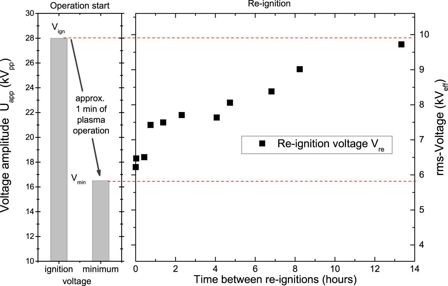
Figure 15. Voltage and net current characteristics of a filamentary DBD in helium–nitrogen gas mixture ( ) operated at 0.5 kHz frequency and 1.75 kV amplitude (top). Grey bars show the time windows (50 μs) for phase-resolved surface charge measurements over a full period of applied high voltage (bottom). Reproduced with permission from [313].
Download figure:
Standard image High-resolution image
Before current pulse appears in the first half period (t = 0–500 μs) surface charges from the previous breakdown (with the opposite polarity) are measured on the electro-optic crystal. In this situation spots of negative charge are obtained, i.e. the electrode covered by the crystal was the anode in the foregoing half period. During the rise of the high voltage slope current pulses are generated and the spots change from negative to a positive surface charge density since the crystal is now the cathodic dielectric. Obviously, the microdischarge inceptions are preferred at positions where discharge events happened in the foregoing half period because the surface charges enhanced the applied field at this location. The surface charges are also inhibiting the formation of microdischarges at the same positions during the same half period. This is apparent from the fact that (1) the spots do not exceed a certain maximum (about 15 C cm−2) and (2) the number of positive spots increases during the rise of high voltage. The surface charge pattern remain constant and thus determine the distribution in the following active phase (t = 1000–1500 μs). A detailed analysis of the surface charge density profiles show a Gaussian distribution with a constant offset value [98, 232, 233]. Both contributions of surface charges are inverted during each following half period. New filaments can occur in the discharge free areas. Sometimes, a filament will not re-ignite at the former position in the following one or more (up to three) periods of the applied voltage. In this situation positive as well as negative surface charge spots are obtained simultaneously but at different locations [232].
Negative surface charges are supposed to be electrons while positive surface charges are assumed to be defect electrons in the dielectric resulting from electron–ion-recombination at the surface [265]. The electron surface layer model in [262, 266] reveals that the axial location of the surface charge along the plasma-dielectric interface region is determined by the electron affinity of the material. The defect electrons are situated in its valence band. The plasma electrons get either trapped in low-energy image potential sites just in front of the crystallographic material boundary (in case of negative electron affinity materials like magnesium oxide) or in the conduction band inside the dielectric with subsequent energy relaxation (in case of positive electron affinity materials like quartz or alumina). The electron affinity of electro-optic crystal has not yet been calculated but the observed stability of the surface charge profiles suggest positive affinity [98]. During the discharge channel formation, the initially accumulated surface charges sidetrack the following charge carriers of the same polarity and thus, the lateral extent of the surface charge spots is determined by the mobility of the responsible charge carriers [229]. The important role of surface processes is also known from investigations of partial discharges where they propagate along the gas-dielectric interface [315]. Beside electron impact ionization charges being produced via surface ionisation due to de-trapping, ion impact and photo effect and attachment of charge carriers at the surface has also to be considered.
The electro-optic measurements discussed above suggest that the surface charges are more or less static. The existence of a constant Ub in case of sinusoidal operation throughout a discharge half period in the equivalent circuit model implies that the microdischarge inception starts at approximately the same threshold, irrespective to the instantaneous value of the applied voltage at the inception time. This behavior is attributed to the existence of the surface charge which is somewhat contradictory to the explanation of multi-filament DBDs [58]. Dedicated electrical measurements in a DBD arrangement with relatively low number of distinguishable filaments combined with the analysis of surface coverage and the statistical distribution of the transferred charge per microdischarge leads to the conclusion that the larger part of the fraction of the deposited charge is mobile on time-scales of hundreds of ns. Such a plasma-induced surface conductivity could explain the offset values of the surface charge profiles [232] as well as the charge transport in case of inhomogeneously charged surfaces obtained in [237]. It would also fit with the proposed deposition of plasma electrons in the conduction band of the dielectric material [262, 266]. However, these electrons can become trapped in localized impurities or intrinsic trap states below the conduction band resulting in the observed 'memory charges' at the filament spots in case of alumina as the barrier material [316–318].
Humidity is known as an important factor in the physics and chemistry of DBDs. For example it tends to increase the current pulse amplitude of a microdischarge [200, 214, 319] induced by a higher surface conductivity [5, 320]. Experimental results on plane-parallel DBDs in helium combined with surface charge measurement have shown a correlation between humidity in the system and the dynamic behavior of filaments [228]. The filaments are non-stationary under humid conditions. The trajectories formed by subsequent filaments resemble a random walk motion. Obviously, the plasma channels evaporate the water film on the dielectric locally. As the water vapor concentration increases the ignition voltage, the filament is not ignited in vapor cloud and the next microdischarge incepts in the adjacent area. This behavior can be regarded as the motion of self-propelled quasi-particles due to mutual interaction of the plasma channel footprints and the surface covered with adsorbed water vapors. The motion stops and a stationary filament is formed when the discharge inception takes place at a location with less humidity at the surface, i.e. where the water film was evaporated by a previous discharge event. Taking this complex and still not fully explored interaction into account, the analysis of the electrical behavior in arrangements with a low number of microdischarges similar as in [58] under controlled gas atmospheres would be beneficial to understand the role of humidity and surface conductivity.
A collective behavior of filamentary volume and surface DBDs in time, i.e. the simultaneous inception of individual microdischarges can be confirmed from synchronized ICCD camera recordings in combination with current measurements [305, 310, 321–325]. From these studies an important role of radiative processes is argued. The VUV emissions from the first microdischarges may lead to photoionisation in the vicinity of the electrodes or to photodesorption of electrons from the charged insulator surface [321, 324]. More details on the role of photoionisation are available from the investigation of corona discharges [301, 326]. In nitrogen–oxygen gas mixtures the number of VUV photons is determined by the nitrogen concentration (atomic lines) while the oxygen concentration determines the absorption length of these photons. Thus, direct photoionisation mechanism is not considered as the dominant source of free electrons, in particular at low oxygen concentrations. Although the mentioned investigations have been performed in air which is known to absorb VUV photons efficiently (mainly by molecular oxygen), there exist photoabsorption windows in the VUV region [321]. A much more pronounced effect could be expected for discharges in noble gases. Here, VUV photons are significantly generated by excimers and less absorbed in the carrier gas [67]. Studies on simultaneous breakdown in noble gases has not yet been performed, but could clarify the role of radiative processes.
The collective behavior of filamentary and patterned DBDs can be influenced by residual species in the volume [60, 303]. At certain overvoltage the formation of microdischarge in the discharge channel from a previous one in the same half period was obtained in coplanar DBDs [327]. It could be confirmed by single microdischarge studies in [328], where a complex branching of discharge channels against the formation of new channels was observed. In [329] the effect of residual heat was considered to lead to the spatial stabilization of the filaments. The increase of temperature and thus decrease of gas density can lead to a significant reduction of breakdown voltage which favor microdischarge inception at the previous position.
5.5. Transition between filamentary and diffuse DBDs
As discussed in section 3.2 the conditions for the operation of DBDs in the diffuse mode are quite specific and determined by the portion between secondary processes at the electrodes and ionisation processes in the discharge volume. The APGD is usually formed in gases with a relatively high gas ionization at comparatively low electric field strength and the ionisation dynamics is further delayed by multistage ionization processes. The content of metastable queching molecules in the gas will therefore determine whether the DBD will operate in diffuse regime or not.
The main feature of the APTD is that the ratio of secondary electron emission at the cathode to the ionization in the discharge volume is relatively high and the metastable  (A) species are considered to enhance secondary electron emission from the cathode (i.e. the previous anode with adsorbed electrons on the surface) [80, 195, 262, 268, 330]. The gas composition also affects the portion of these processes since the effective lifetime of the
  (A) metastables can be significantly reduced by collisional quenching [100, 101]. Another example where secondary electron emission is important are plasma display panel cells [76, 93, 250]. Here, a layer of magnesium oxide which has a high secondary electron emission coefficient is covering the dielectric surface.
A certain overvoltage on APGD or APTD also leads to filamentation. Systematic measurements in [98, 331] have shown that an increase in the voltage slew rate (dV/dt) results in higher power input and thus higher volume ionization which favors filamentation [332]. Filamentary and diffuse mode can coexists in such cases (also called hybrid mode). Due to different secondary electron emission coefficients of materials hybrid modes are obtained in asymmetric discharge cell configurations where filamentation occurs when the electrode with the smaller secondary electron emission coefficient acts as the cathode [98, 236]. Furthermore, the diffuse mode can also show a radial development which is supposed to be correlated with surface processes [88, 98, 237]. In particular in the APGD regime a variety of complex self-organized static or dynamical structures of discharge spots can be observed. Annihilation, motion and self-organization of discharge filaments (typically of reaction-diffusion systems, e.g. hexagons or stripes) can be obtained [13, 332–334]. Experiments and models conclude that filaments are always associated with low current, 'side discharges' that develops in its vicinity beyond the inhibition region. The properties of these side discharges can explain many aspects of filament interactions, dynamics, and pattern formation [333].
Still an open question in DBDs is the role of negative ions on the development and chemistry in gas mixtures containing electronegative compounds. Laser photodetachment of  , and
, and  ions performed on an APGD in helium with admixtures of oxygen shows an influence on the breakdown characteristics which indicates an enhanced pre-ionization by laser detached electrons [335].
6. Conclusion and perspectives of DBD research
Although used since more than hundred years DBDs are still one of the most important technological plasma sources for the generation of nonthermal gas discharges at atmospheric pressure. Researchers have been able to adapt the DBD principle on many different tasks and objects. The presented collection of DBD arrangements in this review is aimed to inspire further novel designs and solutions toward the handling of technical challenges in the future. These are mostly in the field of chemistry (e.g. removal of pollutants, plasma synthesis), life-science (e.g. decontamination, would healing and other therapies) and flow control.
DBDs are well-scalable, robust and good-controllable plasma sources. Thus, the interest on the development of new sources and understanding its fundamentals will continue. The further miniaturization of plasmas towards higher surface-to-volume ratios could enable new and more efficient processes. The evolving opportunities of nano-technology will enable the development of new diagnostics and more sophisticated plasma sources. Novel power sources give the chance to control plasma parameters and to enhance the efficiency.
The development of new DBD reactors or treatment devices should always be accompanied by a reliable characterization. In particular the electrical characterization sketched here and in the cited literature should be mandatory. In connection with other diagnostics and simulation this relatively simple technique allows not only a macroscopic characterization, but also further insights on the plasma properties and dynamics. Understanding the microdischarges as the most fundamental elements of a DBD process is one important key for the optimization of existing processes and the development of new applications. Nowadays, several techniques enable the desired sensitivity and time resolution for the study of the development of these transient discharges and the determination of the basic plasma parameters. Following and intensifying the discussed work will open up more possibilities for application and research. In particular the merging of single microdischarge studies with multi-filament DBDs is still an open question and requires different approaches, including theory, modeling and experimental work. Other open questions regard the role of radiative processes, surface properties, and humidity in the system. Dedicated experiments under well-defined conditions are required for further insights.
The relevant processes in DBDs and other nonthermal plasmas are characterized by different time scales. The 'volume memory processes' are connected with the recombination of charge carriers in the discharge gap and thus, typically proceed in the range of microseconds. The 'surface memory processes' are related to the amount of surface charges and the mechanisms of charge trapping and transport on dielectric surfaces. The typical timescales are in the range of seconds or higher. But even faster surface processes are under discussion and the understanding of plasma-surface interaction in these discharges deeper is still a big scientific challenge. This is also the case for the investigation of different discharge modes and operation regimes. A much larger diversity of this is known today than twenty years ago and researchers are capable to control and reproduce patterned and diffuse DBD modes. The control of DBD uniformity is not only important for its exploitation in surface processing but also a fundamental question for gas discharge physics. Today much more is known about the microphysical processes in these plasmas and at the plasma-surface interface, but it should be extended to more complex boundaries, e.g. catalytic surfaces or liquid layers.
To remember the situation in the ozone generator research in the 1970s at this time, it was not expected that basic research on a discharge known about for more than 100 years could have far-reaching technological and economic consequences. However, the efficiency of such generators was significantly improved and DBDs have opened up many new applications in the following years. It seems that this evolution is still going on.
Acknowledgments
With deepest gratitude and respect I dedicate this review to Dr Ulrich Kogelschatz (1937-2016). Our community will miss his input and support.
The author expresses his gratefulness to all colleagues and cooperation partners. In particular Hans Höft, Marc Bogaczyk, Tomas Hoder, Manfred Kettlitz, Wolfgang Reich, Michael Schmidt, Andrei Pipa, Torsten Gerling, Detlef Loffhagen, Markus M Becker, Jan Schäfer, Lars Stollenwerk, Franz X Bronold, Robert Tschiersch, Sebastian Nemschokmichal, Robert Wild, Peter J Bruggeman, Hans-Erich Wagner, Kirill V Kozlov, Jürgen F Kolb, Jürgen Meichsner and Klaus-Dieter Weltmann are acknowledged for fruitful cooperation and support.
Part of the work shown here was supported by Deutsche Forschungsgemeinschaft (DFG, TRR 24 'Fundamentals of Complex Plasmas'), the Federal German Ministry of Education and Research (BMBF, grants 03FO1072 and 13N11188) and the Ministry of Education, Research and Culture of the State of Mecklenburg-Vorpommern (grant AU 07139).