

Abstract
The most efficient earth abundant, non-toxic thin film multelemental PV devices are fabricated from Cu, Zn, Sn, S and Se, with the chemical formula of Cu2ZnSn(SxSe1−x)4 (CZTS,Se). This material has enjoyed relatively rapid increases in efficiency from its inception to its present-day power conversion efficiency of 12.6%. But further increases in efficiency have been hampered by the inability to substantially increase Voc, the open circuit voltage. In this review article we will discuss the fundamentals of this important kesterite material including methods of film growth, post growth processing and device fabrication. Detailed studies of the properties of CZTS,Se including chemical, structural and electronic as well as full device electrical characterization have been performed in an effort to coax out the critical issues that limit performance. These experimental studies, enhanced by density functional theory calculations have pointed to fundamental bulk point defects, such as Cu–Zn antisites, and clusters of defects, as the primary culprits in limiting Voc increases. Improvements in device performance through grain boundary passivation and interface modifications are described. Exfoliation of functioning solar cells to expose the back surface along with engineering of new back contacts designed to impose electrostatic fields that drive electron-hole separation and increase Voc are discussed. A parallel route to increasing device performance by alloying Ag with CZTS,Se in order to inhibit Cu–Zn antisite defect formation has shown significant improvement in material properties. Finally, applications of high S (and hence higher Voc) CZTS,Se based devices to energy harvesting for 'Internet-of-Things' devices is discussed.
Export citation and abstract BibTeX RIS
Introduction
At present the solar cell industry is growing exponentially in response to the need for renewable energy sources worldwide. The predominant material used for this dramatic increase in utilization is Si, with present module/panel efficiencies nearing 20% [1]. Given the substantial availability of Si in the earth's crust (typically found in its oxidized form) Si based photovoltaic (PV) devices will continue to dominate the industry for large scale use. But Si suffers from two fundamental constraints—it is an indirect band gap material requiring the Si absorber thickness to be ∼300 micrometers (μm) for complete absorption of sunlight and its refinement into an electronic grade single or polycrystalline material is energy intensive. Reduction of Si from SiO2 can require furnace temperatures in excess of 1500 °C to achieve the required purity.
An alternative to bulk PV materials such as Si are the class of thin film PV absorbers fabricated from strongly absorbing, direct band gap materials. These materials offer the prospect of substantially thinner (∼1–2 μm) devices that typically involve less energy intensive fabrication. The most successful thin film absorbers for PV are typically multi-elemental compounds or alloys. To date the most efficient multinary, or multi-elemental, thin film PV devices in commercial use today include binary and ternary compounds such as GaAs, CdTe, GaInAs, and more complex compounds such as CIGSe (Cu,In,Ga,Se). III–V based PV devices exhibit the highest single junction efficiencies [2] (∼28%) but are extremely expensive to manufacture since they are typically grown on single crystal substrates. CIGSe and CdTe are somewhat less efficient (∼22% as of this writing) but far less expensive, and arguably easier to manufacture. Both of these technologies, though, suffer from limited elemental abundance in the earth's crust (In, Te, Ga), and are mined in relatively small quantities [3]. As an example, examination of the US Geological Survey3 shows that only 820 metric tons of In were mined in 2014 (spot price ∼$700/kg) compared with more than 26 000 tons of Ag. In and Ga are also subject to substantial competition from use in the electronics industry, eventually limiting scalability of this material for giga- and terawatt power production. An additional disadvantage for CdTe is the toxicity of Cd metal as well as Te, leading to concerns about its widespread use in the environment. Nonetheless solar cells are being manufactured with these materials at the module scale. Another candidate thin film absorber, Pb based organic/inorganic hybrid perovskites have achieved over 20% efficiency [4], but suffers from long term efficiency instability and toxic and water soluble Pb. From an industrial perspective, wide-scale deployment of PV devices for energy generation and for powering autonomous computers and sensors demands stable, non-toxic materials.
To date the most efficient earth abundant, non-toxic multinary thin film PV devices are fabricated from Cu2ZnSn(Sx,Se1−x)4, CZTS,Se. Despite PV efficiency records of slightly more than half that of both CIGSe and CdTe, this PV absorber may eventually achieve improved performance through additional alloying and/or novel device architectures to compete with other technologies. Detailed studies of the defects in this material have shed new light on potential paths for improvement. It is the intent of this review article to describe some of the many investigations that have illuminated the problems and issues of CZTS,Se and approaches taken to improve the performance of devices fabricated from this absorber. Some of these approaches include, as we will discuss, modification of the back contact of CZTS,Se based devices and substitutional alloying with Ag in an effort to address bulk point defect limitations. In this topical review we will briefly discuss the historical evolution of CZTS,Se from its low efficiency beginnings [5, 6] to its present day peak of 12.6% [7]. We will detail our fundamental understanding of factors that limit increases in efficiency, due in great part to bulk point defects, primarily Cu/Zn antisite defects and clusters of defects. A combination of electrical, optical and electronic characterization is coupled with device simulations and ab-initio calculations to identify the fundamental bulk properties and performance limitations associated with these defects. We will discuss our understanding of grain boundaries, non-radiative recombination and the resulting increase in device performance following treatments that passivate grain boundaries and surfaces.
We will describe studies of the p–n heterojunction and the determination of the valence and conduction band offsets measured with femtosecond ultraviolet photoelectron spectroscopy (fs-UPS) coupled with optical spectroscopies. We will also describe experiments involving exfoliation of full devices that reveal the back absorber surface and our recent experiments designed to study and engineer the back contact to increase open circuit voltage, Voc. Finally we will describe our most recent modifications of the bulk absorber by alloying CZTS,Se with Ag that inhibit anti-site defect formation [8]. Ag-alloying has led to high device efficiencies and shows substantial promise for achieving even further efficiency increases through process optimization. As an example we have achieved a low temperature (<200 K) efficiency of 16.2% for the alloy Ag0.1 Cu0.9 ZTSe, which stands as the highest efficiency achieved to date, at any temperature, in the earth abundant kesterites and suggests the possibility of eventual increases in efficiency beyond 12.6% at room temperature. In addition to devices alloyed with Ag, pure AgZTSe devices have been fabricated, with efficiencies in excess of 5% [9]. All efficiencies discussed in this review are for 0.45 cm2 cell size.
A brief history of CZTS,Se
Early synthesis of CZTS was reported by Ito [10] in 1988 via vacuum deposition techniques. Additional papers chronicling the progress of CZTS [5, 11] appeared in subsequent years. In 2010 at IBM, a breakthrough in both the efficiency and method of deposition employed solution techniques utilizing hydrazine as the solvent [12]. This approach involved dissolution of metal precursors in hydrazine to form an ink that was subsequently spun onto Mo coated soda-lime glass (SLG) in multiple layers and achieved an efficiency of 9.6%. Further refinement of the process led to even higher efficiencies; 10.1% [13] in 2012, 11.1% also in 2012 [14] and finally 12.6% [7] in 2014.
While vacuum deposition approaches [15] (Repins, 9.15% in 2012) have advanced to a present value of 11.6% [16] reported in 2015, solution deposition has still produced the highest efficiency to date. This result is in contrast with all other thin film materials where vacuum or sputter deposition approaches have achieved the highest performance in PV devices.
From the commercial/industrial perspective, large area films can be deposited either by sputtering [17–20], spin coating [7, 13], spray coating [21–24] or doctor-blading [25–29] the precursors onto the appropriate substrate reducing the manufacturing costs of large area PV modules. While sputtering is a vacuum process that inherently may be more expensive, spin, spray and doctor-blade coating of substrates are all low cost manufacturable approaches. Other more benign solvents such as water [11, 30] and DMSO (dimethyl sulfoxide) [28, 31–33] have also been utilized in an effort to avoid the use of hydrazine. To date, though, spin coating with hydrazine as the solvent has produced the highest efficiencies. This significant advantage though, is mitigated by the reluctance of this material to perform at ever higher efficiencies through processing improvements. As we will discuss in this article, the formation of unavoidable fundamental bulk defects is primarily responsible for limiting efficiencies. Nonetheless, CZTS,Se and its newer alloys with Ag are compelling technologies that, as with many reluctant materials, will yield to improvements in time as we obtain greater insight into the factors that limit efficiency.
Kesterite fundamentals
The basic kesterite unit cell is shown in figure 1. Cu atoms (orange) exist in the 1+ oxidation state, Sn(blue) in the 4+ state, Zn(silver) in the 2+ and S and/or Se (yellow) in the 2-state. Stoichiometric CZTS,Se is written as Cu2ZnSn(Sx,Se1−x)4. As we will discuss, off-stoichiometry, Cu poor films are required to fabricate functioning devices. As shown in the unit cell we have identified within the dashed circle a plane of Cu and Zn atoms. Cu and Zn, in addition to being neighbors in the periodic table, have nearly identical covalent radii, differing by only 2 picometers.
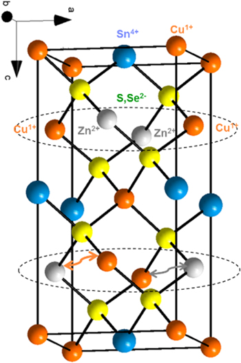
Figure 1. Kesterite unit cell with Cu (orange), Zn (silver), Sn (blue) and S/Se (yellow). Arrows indicate Cu/Zn site swapping (antisite defect formation) as discussed in the text.
Download figure:
Standard image High-resolution imageHigh temperature anneals (hard bake (HB)) at 550–600 C are required to coarsen the grains in the polycrystalline absorber and the result is nearly complete site disordering of the Cu and Zn occupancy along this plane within the unit cell [34–37]. These antisite defects lead to a smearing of the band edge (band tailing) that reduces open circuit voltage (Voc) as will be discussed later in this article.
Growth modes
Fabrication of CZTS,Se films has typically proceeded along two fronts. The first involves co-evaporation of the elemental constituents onto a Mo coated SLG substrate. Carefully controlled fluxes of the elements from effusion cells are directed toward the substrate typically held at elevated temperature [15, 16, 38]. A variety of approaches include growing at modest substrate temperatures (∼150 C) to mitigate Se loss [16, 38] followed by high temperature anneal. Repins et al [15] carried out growth at elevated temperatures (>500 C) with a significant background flux of Se and Zn during growth and cool-down. In the former case, a post-deposition anneal or 'HB' is used to coarsen the grains to achieve sizes in the 1–2 μm range. A cross-sectional scanning electron microscope (SEM) image of vacuum deposited CZTSe that achieved an efficiency of 11.6% [16] is shown in figure 2.
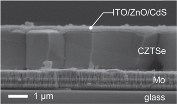
Figure 2. Cross-sectional SEM of vacuum deposited CZTSe leading to an 11.6% efficient device (from [16] John Wiley & Sons. [© 2014 WILEY-VCH Verlag GmbH & Co. KGaA, Weinheim]).
Download figure:
Standard image High-resolution imageA second approach, and one that has achieved a series of record efficiencies [7, 12, 13], with the highest presently at 12.6% [7], involves deposition from a liquid ink (figure 3). In this technique, metal precursors are dissolved in hydrazine to form the ink and are subsequently deposited onto a spinning substrate. Multiple layers are spun on followed by low temperature anneals designed to drive off the hydrazine solvent. Deposition is carried out in a N2 glove box for both isolation of the hydrazine which is toxic and explosive, as well as minimizing contamination of the absorber layers. Subsequent to the deposition of a complete series of layers, the film undergoes a HB at ∼600 C to further crystalize the film.
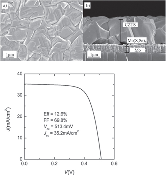
Figure 3. Top: top down and cross-sectional SEM images from CZTS,Se absorber. Bottom: J–V measurements from 12.6% device (from [7] John Wiley & Sons. [© 2013 WILEY-VCH Verlag GmbH & Co. KGaA, Weinheim]).
Download figure:
Standard image High-resolution imageThe basic device fabrication is shown in figure 4. Following ink deposition and anneal, an air anneal is carried out, to be discussed later. The n-type buffer, typically CdS, is deposited in a chemical bath at ∼80 C. The thickness of the CdS layer varies but can be anywhere from 25–100 nm. Since CdS possesses a band gap of 2.4 eV it absorbs in the blue range of the solar spectrum and so it is advantageous to keep it as thin as possible.

Figure 4. Basic schematic of a CZTS,Se PV device.
Download figure:
Standard image High-resolution imageFollowing CdS deposition a thin layer of ZnO is sputter deposited followed by conductive indium tin oxide used to transport electrons to an array of thin NiAl wires. An optimized transparent conducting oxide stack has been described by Winkler [39].
The most important interfaces are the CZTS,Se/CdS p–n junction and the rear contact (CZTS,Se/Mo) and we will discuss experiments designed to optimize both. But it is bulk defects within the CZTS,Se that limit improvements in both voltage and efficiency of these devices.
Bulk defects
Returning to our earlier discussion of why the Voc deficit, defined as Egap–Voc, is so difficult to improve, we look in greater detail at the unit cell of figure 1. As mentioned, Cu and Zn can swap sites quite easily during high temperature anneals. Other point defects can also exist including Zn and Cu vacancies and deeper defects such as Sn and Cu antisites [40, 41].
Energetically favorable defect clusters can also be found within the grains of these films. Defects are shown [40] in figure 5 calculated using density functional theory that reveal their energetic location within the band gap of CZTS.
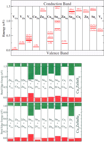
Figure 5. Top: energetic locations of various point defects within the CZTS band gap. Bottom: energetic locations of defect clusters. Reprinted figure with permission from [41], copyright (2010) by the American Physical Society.
Download figure:
Standard image High-resolution imageIn addition to this large set of bulk defects, the phase diagram of CZTS,Se provides for a very narrow concentration range in which CZTS,Se is stable [42]. In particular, Chagarov et al has shown [42] that a combination of elemental mixing and lattice vibrations at elevated temperatures, typical of HB anneals (∼900 K), helps to stabilize the CZTS0.25Se0.75 phase; this S,Se alloy is similar to that used in the record 12.6% device. Figure 6 shows that for Gibbs mixing plus lattice vibrations, the size of the region for the existence of the stable kesterite phase of CZTS0.25Se0.75 at 300 K is smaller than that at 900 K.
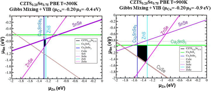
Figure 6. Phase space calculation showing that the region of stability for the formation of CZTS0.25Se0.75 with Gibbs mixing plus lattice vibrations at 300 K (left) is substantially smaller than that at 900 K (right). Reprinted with permission from [42]. Copyright (2016), AIP Publishing LLC.
Download figure:
Standard image High-resolution imageOutside of these conditions, secondary phases can and do form [40]. Obtaining the correct location in the phase diagram requires careful choice of annealing conditions and times as well as elemental concentrations in the precursor ink. Furthermore, it has been determined that Cu poor concentrations in the film are required to achieve the highest efficiencies. The Cu concentration impacts the majority carrier density (holes for this p-type material); too high a carrier density can dramatically shorten the width of the depletion field at the p–n junction limiting carrier collection. Too high a carrier density can lead to significant shunting of the device.
Experimental evidence for the high density of bulk defects and their impact on device characteristics is shown in figure 7. Gokmen et al [43] compared internal quantum efficiencies (IQE) between CIGSe and CZTS,Se devices. While the short wavelength behavior from both materials is nearly identical, the long wavelength region reveals significant differences.
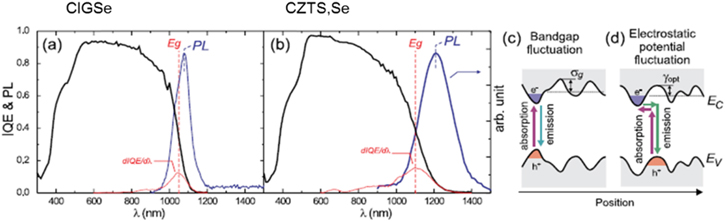
Figure 7. Left: quantum efficiency comparisons of CIGSe and CZTS,Se devices. Right: models comparing band gap fluctuations and electrostatic potential fluctuations deriving from charged defects. Reprinted with permission from [43]. Copyright (2013), AIP Publishing LLC.
Download figure:
Standard image High-resolution imageReferring to figure 7, first note that for CIGSe the long wavelength edge drops sharply and the peak of the PL emission is energetically close to the band gap. The sharpness of the edge indicates that there is little band tailing while the small energy difference between the PL peak and the band gap (shown in red) emphasizes that defects that do exist within the band gap are close to the band edges (shallow). Furthermore, the width of the PL peak is also consistent with a very narrow defect band that sits just below the band edge.
In contrast the IQE for CZTS,Se shows a broadened long wavelength edge, a PL peak energetically further removed from the band edge and a PL width significantly larger than for CIGSe. These results draw a stark contrast between the two materials and suggests that the dramatic difference in efficiencies is a consequence of the defect properties of the bulk material. The schematic on the right side of figure 7 draws a comparison between band gap fluctuations (regions of differing elemental concentrations leading to different band gaps) and electrostatic fluctuations due to charged defects. In order to discern the difference in mechanisms, carrier lifetimes were measured at low temperatures. At 4 K it is expected that electrostatic fluctuations would result in substantially increased lifetimes since electrons and holes relax into spatially separated valence and conduction band local minima; the lack of thermal energy localizes these carriers in wells that require tunneling to facilitate recombination. In the case of band gap fluctuations electrons and holes are not spatially separated and lifetimes are not expected to increase substantially. It is observed [43] that lifetimes measured at low temperatures are much longer in CZTS,Se (on the order of μs) indicating that photogenerated electrons and holes occupy deep trap states that are spatially separated, consistent with electrostatic fluctuations as the primary source of the long wavelength slowly decaying edge. This in turn indicates that the substantially greater density of bulk defects in CZTS,Se relative to CIGSe explains a primary reason for the efficiencies in the respective devices. A substantial body of literature points to considerable disorder due to Cu–Zn antisite defects in CZTS,Se [34, 35, 44–48]. Approaches to dealing with bulk defects will be discussed later in this paper.
Interfaces and band offsets
Another key issue involves the p–n junction, both in terms of the interface quality and the band offsets. In particular, for a high efficiency device, the conduction band minimum (cbm) of the n-type buffer (in this case CdS) must be slightly higher (spike) than that of the p-type CZTS,Se. At first blush one may question why a small barrier to electron flow from the absorber to the buffer is required. The reasons for this are two-fold. The first is that a buffer cbm below that of the absorber (cliff) can reduce Voc by enhancing e–h non-radiative recombination. Second, a spike offset removes electrons from the CZTS,Se/CdS interface and reduces the non-radiative e–h recombination that would dramatically reduce Jsc at the interface. Spike barriers up to ∼0.4–0.5 eV are beneficial [49]; beyond this level higher barriers can reduce current flow and hence efficiency.
Measuring the band offsets between absorber and buffer typically involves sequential depositions of thin layers of buffer material followed by monitoring of the bulk atomic core levels with x-ray photoelectron spectroscopy as they shift in response to charge transfer between buffer and absorber- band bending. This can be laborious and in the case of CBD deposition extremely difficult as the sample must be removed from the vacuum analysis chamber for each additional buffer deposition.
A unique approach (figure 8) involves utilizing pump/probe femtosecond laser photoelectron spectroscopy or fs-UPS [50–52]. The fs-UPS technique utilizes fs pulses from an amplified Ti:sapphire laser system whose output is split into pump and probe arms. The probe pulses are frequency upconverted to photon energies ranging from 15 to 40 eV for UPS by high harmonic generation in Ar gas; individual harmonics are spectrally selected and focused onto the sample in an ultrahigh vacuum analysis chamber and produce 'standard' UPS spectra. To extract the band bending at the CZTS,Se junction, time-correlated 1.55 eV (800 nm) pump pulses are focused on the probe area; the resulting dense e–h population created in the CZTS,Se screens the static dipole field in the depletion region and flattens the bands, causing a rigid energetic shift of the UPS spectrum. The laser intensity is sufficient to fully flatten the bands and the bending is extracted by measuring the magnitude of the shift.
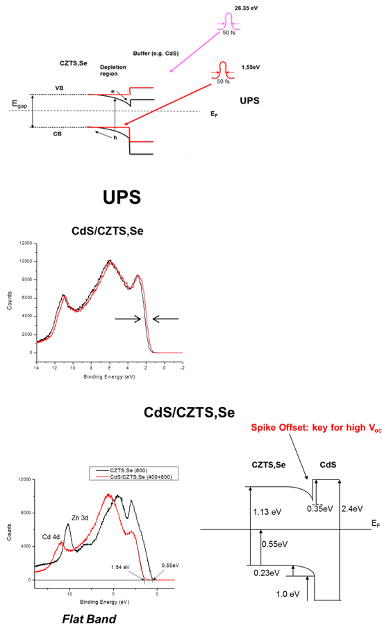
Figure 8. Top: band schematic showing the junction region. 1.55 eV pump photons flatten the bands while a time synchronized 26.35 eV pulse of light is used for UPS. Below shows the comparison of unpumped(black) and pumped (red) spectra. Bottom left: overlap of flatband bare CZTS,Se (black) and 20 nm CdS/CZTS,Se (red). Right: band diagram with band bending extracted from the spectral data. Reproduced with permission from [53].
Download figure:
Standard image High-resolution imageUnder flatband conditions the location of the clean CZTS,Se vbm can be determined relative to the Fermi level(figure 8) and the same for the CdS/CZTS,Se vbm. The clean CZTS,Se surface was obtained by etching in dilute NH4OH to remove oxides, followed by a rinse in deionized water. Following insertion into the vacuum analysis chamber a mild 120 C anneal removed surface adsorbed water. Interestingly the bands at and near the clean CZTS,Se surface are bent upward slightly in accumulation [54]. Under flat band conditions the Fermi level is found near the center of the band gap consistent with a high density of compensating defects. The observation of a mid-gap Fermi level and the inability to dope and then move the Fermi level to a more p-type position relative to the vbm contributes to the difficulty in achieving higher Voc [54].
Once the vbm positions are known, the cbm positions are then determined from the knowledge of the band gaps of both CZTS,Se and CdS as shown in figure 8. This set of measurements provides the Fermi level of the system, band bending and valence band locations as well, so that the electronic alignment of the system is fully determined. With this approach the band offsets have been determined for a series of buffer materials including CdS [51], ZnO, ZnS, In2S3 on CZTS,Se [52] and Zn(O,S)/SnS [55].
The role of grain boundaries
Grain boundaries are ubiquitous in polycrystalline thin film PV absorbers and are of key concern. A high density of small grains can degrade device performance since vertical current flow involving holes transiting to the back contact and electrons to the p–n junction at the front, would require carriers to cross multiple grain boundaries. This would result in increased e–h recombination and scattering at each grain boundary crossing with resultant loss of current and voltage. As such it is crucial that material processing produces individual grains sufficiently large to span from the bottom contact to the top. It was shown early on that Na diffusing out from the SLG substrate was instrumental in enlarging grains to the 1–2 μ scale [56–59].
Passivation of grain boundaries is a critical area since recombination of electrons and holes at these boundaries can dramatically affect device efficiency. It was found that passivation of the grain boundaries through an anneal in air following a HB increased PL as well as device efficiency [54]. This anneal is carried out in air in the range from 250–400 C for several minutes. During this anneal, oxygen can diffuse along grain boundaries forming a Sn-rich oxide passivating layer between the grains. Air annealing (AA) has been shown to both dramatically increase PL and device efficiency [54]. Figure 9 top, shows the comparison of PL from a CZTS,Se film collected before and after air anneal.
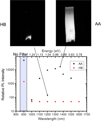
Figure 9. Top: PL image of a CZTS,Se film before (left) and after (right) air anneal. HB refers to hard bake alone while AA refers to hard bake + air anneal. Bottom: relative PL intensity as a function of wavelength. Reprinted with permission from [54]. Copyright (2014), AIP Publishing LLC.
Download figure:
Standard image High-resolution imageSpectral results displayed in figure 9 bottom show a peak in the PL at 0.96 eV in good agreement with spectra collected in a typical PL spectroscopy tool [60]. In order to determine the chemical composition of the surface and grain boundaries in CZTS,Se Auger nanoprobe (nanoAuger) [61] images were collected from the top and in cross-section following AA (figure 10). As can be seen, while the grain boundaries are Cu depleted, both Sn and O are observed to accumulate there indicating the formation of Sn oxide.

Figure 10. NanoAuger data showing Cu depleted grain boundaries, Sn and O rich grain boundaries following air anneal. Elemental compositions corresponding to specific points (SEM on left) are shown in the table (from [61] John Wiley & Sons. [© 2015 WILEY-VCH Verlag GmbH & Co. KGaA, Weinheim]).
Download figure:
Standard image High-resolution imageThe presence of the SnOx at the grain boundaries correlates strongly with an increase in PL and device performance [61]. Upward band bending at the grain boundary drives minority carriers from the interface, dramatically reducing e–h recombination there and enhancing PL intensity. As a result, AA of the CZTS,Se films produces a several percent increase in efficiency and is now a fundamental part of the device fabrication process. As can be seen in figure 10 following AA, the grain boundaries are Cu poor, Sn and O rich indicating the formation of tin oxide that acts as a barrier to recombination, thereby decreasing non-radiative e–h recombination at grain boundaries. An additional effect may involve incorporation of O into the near surface region, widening the band gap there and repelling holes [62]. It is clear that oxidation reduces e–h non-radiative recombination leading to increased film PL and device performance.
Back contact engineering
Now that bulk defects, interfaces and grain boundaries have been studied and discussed in considerable detail, and their impact on device performance is arguably better understood, we focus on ways to improve the efficiency of CZTS,Se based solar cells. One approach is to address the key issue of bulk defects that, as we have discussed result in band tails that narrow the band gap and lower Voc. One approach to mitigating the formation of Cu–Zn antisite defects is through the incorporation of Ag whose larger covalent radius increases the barrier to antisite formation. This will be discussed in the next section. Another approach is through back contact engineering involving the imposition of an electrostatic field that drives the separation of electrons and holes and this is discussed in this section.
The physics of back contact engineering is captured in figure 11. In essence, a high work function (HWF) material such as MoO3 deposited onto the back of CZTS,Se results in electron transfer from CZTS,Se to the MoO3 as the Fermi levels of the two materials equilibrate. This in turn generates an electrostatic field within the CZTS,Se that drives electrons away from this interface and toward the p–n junction. Fs-UPS confirms that this charge transfer and subsequent band bending does indeed occur.
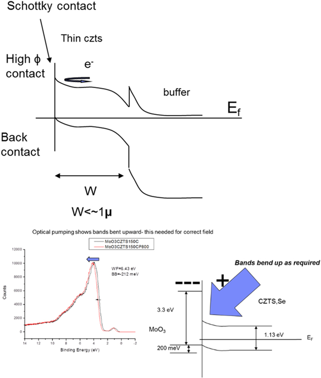
Figure 11. Top: schematic showing band bending near rear surface of device associated with electron transfer from the lower work function CZTS,Se (5.2 eV) to the high work function MoO3(6.5 eV). Bottom left: fs-UPS showing that the bands bend upward at the MoO3 interface. Black spectrum is unpumped and red spectrum is pumped CZTS,Se. The shift to higher binding energy following pumping indicates the bands are originally bent upward. The direction and magnitude of the band bending are shown in the bottom-right schematic.
Download figure:
Standard image High-resolution imageMoO3 has been studied widely [63, 64]. It evaporates congruently as MoO3 but oxygen vacancies are typically present in the film leaving it sub-stoichiometric; this is actually advantageous since this leaves the film more conductive. Our UPS based measurements reveal that the as-deposited films exhibit a work function of ∼6.5 eV, although caution must be used to prevent air exposure as this precipitously drops the work function by as much as 1 eV.
As can be seen from the spectrum (figure 11) pumping of the MoO3/CZTS,Se interface shifts the spectrum to higher binding energy indicating that the unpumped bands are bent upward. The upward band bending is a result of an electrostatic field that drives electrons toward the front of the device creating an electron mirror that increases Voc and reduces recombination at the back interface.
With the presence of a field at the back contact, the question as to how to further capitalize on this effect arises. In order for an increase in Voc and hence efficiency to occur the absorber thickness must be tailored to exploit this. Two additional factors must be accounted for, including the carrier diffusion length and the depletion width near the p–n junction. As a result the absorber thickness (Labs) must be smaller than the sum of the front contact depletion width (LdepF), back accumulation width (LaccumB) and the carrier diffusion length (Ldiff). We can write a simple equation that states

Ldiff ∼ 1 μm [65] while the depletion width near the p–n junction is 200–300 nm and accumulation width < 100 nm near the back contact. This implies that the absorber thickness must be below ∼1–1.5 μ before increases in Voc would be noticeable. This result is confirmed with device simulations (WXAmps) [61, 66], shown in figure 12. The input parameters for WXAmps were based on simulations that fit the 12.6% efficient device. These included a CZTS,Se band gap of 1.13 eV, a 25 nm thick CdS buffer layer, electron and hole mobilities of 100 and 25 cm2 V−1 s−1 respectively and a spike conduction band offset between CdS and CZTS,Se of 0.35 eV. At 2 μm absorber thickness little difference is observed between the HWF, reflective back contact and the standard Mo back contact. But below ∼1.5 μm WXAMPS predicts a continuous increase in Voc, with substantial increases occurring below 1 μ.

Figure 12. WXAmps device simulations comparing Voc for a standard PV device (black squares and red circles) as the absorber is thinned and one with a high work function back contact (green and blue triangles). FB refers to flat band (MoS2 or MoSe2) and reflectivities (R) are either 1 for a highly reflective back contact or 0 for a non-reflecting contact (from [61] John Wiley & Sons. [© 2015 WILEY-VCH Verlag GmbH & Co. KGaA, Weinheim]).
Download figure:
Standard image High-resolution imageAlthough back contact modification can be carried out in the 'substrate' mode where the CZTS,Se is deposited atop the HWF layer, the required high temperature anneals to crystalize the CZTS,Se results in degradation of the HWF layer due to elemental diffusion. To deal with this issue, we instead grow a full CZTS,Se solar cell and separate (exfoliate) the active device from the Mo/glass substrate. In this 'superstrate' process, a thin piece of fused silica is epoxied atop the device and exfoliation is carried out with a mechanical impulse as shown in figure 13.

Figure 13. Schematic showing process by which the CZTS,Se PV device is removed (exfoliated) from its Mo/glass substrate, followed by deposition of a high work function MoO3 layer plus Au.
Download figure:
Standard image High-resolution imageThis process exposes the back surface of the CZTS,Se absorber and experiments have shown that no residual Mo is present. A new back contact consisting of a 10–70 nm MoO3 layer and a thicker layer of Au are deposited at or near room temperature as shown in the figure 13 and additional 'superstrate' measurements are carried out.
Actual measurements of Voc, as shown in figure 14 reveal that Voc increases with decreasing absorber thickness. The data (black squares) all lie below the actual WXAmps simulation suggesting that this difference arises from the lack of complete passivation of the back surface in the actual devices.
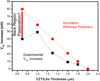
Figure 14. Comparison of WXAmps simulation (red) and experimental exfoliated device results for Voc for increasingly thinner CZTS,Se films with high work function, reflective back contacts.
Download figure:
Standard image High-resolution image
Figure 15. CZTS,Se unit cell showing the incorporation of Ag whose larger covalent radius inhibits antisite formation.
Download figure:
Standard image High-resolution imageRecent results have shown all-around improvement in device performance including Voc, fill factor (FF), Jsc and efficiency. In addition to the increase in Voc as we have just described, FF improves due to the removal of the original back contact that may contain secondary phases that lead to increased non-radiative e–h recombination and hence reduced series resistance. Jsc is observed to improve due to the index matching properties of the epoxy that reduce reflection of incoming light.
Elemental substitution-Ag alloying
Another approach to improving efficiency involves reducing the impact of bulk defects by addressing the specific issue of anti-site defect formation. As discussed previously, Cu and Zn are neighbors in the periodic table and possess nearly identical covalent radii. Following high temperature processing, Cu and Zn are nearly completely site disordered. Ag is a promising cation substitute for Cu in both an alloyed and pure kesterite crystal since it is isoelectronic with Cu, but possesses a covalent radius that is ∼15% larger (see figure 15). Chagarov [67] and separately Yuan [68] have calculated a barrier to Ag/Zn site exchange that is 2–3x larger than that for Cu/Zn exchange that would lead to a lower antisite defect density by a factor of 10.
Improvement in the fundamental properties of AZTSe films is evidenced in the characterization experiments shown in figure 16. In the top left figure, AZTSe, possessing a band gap of 1.33 eV exhibits a PL peak just a few meV below the band edge. In contrast CZTS,Se exhibits a PL peak as much as 200 meV below the band edge indicating that AZTSe possesses primarily shallow defects. This is confirmed in figure 16 (top right and bottom) where the AZTSe PL spectrum is both substantially narrower than CZTS,Se and spectrally similar to CIGSe.
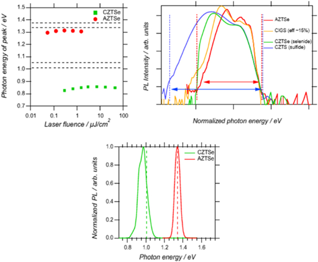
Figure 16. Top left: location of PL peak relative to band edges for CZTSe (green) and AZTSe (red). Top right: PL spectra of AZTSe (red) in comparison with CIGSe, CZTS and CZTSe showing significant narrowing of the PL emission. Bottom: PL from CZTSe and AZTSe reflecting differences in band gaps of the materials but also revealing a more narrow peak for AZTSe than for CZTSe. Reprinted with permission from [67]. Copyright (2016), AIP Publishing LLC).
Download figure:
Standard image High-resolution imageWhile characterization of fundamental properties of AZTSe indicates significant improvement in many of the defect related issues that limit CZTS,Se such as band tailing, a drawback is that as-grown and annealed AZTSe is n-type [69]. In addition to being n-type, AZTSe possesses an extremely low intrinsic carrier density, ∼1012 cm−3. By virtue of its n-type nature, the choice of available and well-understood p-type buffers necessary to form a good p–n junction is limited. To date, the most successful devices, achieving just above 5% efficiency [9], have been fabricated in a structure that consists of a fluorinated tin oxide coated glass substrate as a rear contact, AZTSe absorber and a top layer of MoO3 forming a 'Schottky-type' front contact. The search for an appropriate wide band gap p-type buffer is ongoing.
While pure AZTSe is an extremely promising absorber, alloying Ag with Cu to form the compound (AgxCu1−x)2ZnSnSe4 has also been explored [70–74]. Early work was carried out on this alloy by Gong [75] and Tauchi [76]. These studies showed the kesterite nature of the alloy and mapped the band gap that appeared to narrow slightly at low Ag concentrations before increasing monotonically at higher concentrations to the pure Ag value of 1.33 eV.
Tauc plots (figure 17(a) top) reveal an increase in the band gap with higher Ag content in the alloy to a maximum of 1.33 eV for full Ag [69]. The peak PL positions for each alloy are shown in figure 17(a) bottom. Note that the difference between the PL peak energy and the band gap decreases with increasing Ag content. This is shown quantitatively in figure 17(b) where the PL peak energy (open squares) is subtracted from the band gap (Eg solid black dots) to produce this energy difference (red x's). Note that this difference drops monotonically from 110 meV for full Cu to essentially 0 meV for full Ag indicating that band tailing is continuously reduced for increasing Ag content. This correlates with the expectation that Ag inhibits the formation of antisite defects and is further evidence that Cu–Zn antisite formation is largely responsible for band tailing and Voc limitation.
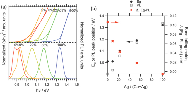
Figure 17. (a) Top: normalized Tauc plots from UV–vis measurements as a function of Ag/(Ag+Cu), bottom: normalized PL. (b) Plot of band gaps (black dots), PL peak positions (open squares) and Eg-PL (red x's) as a function of Ag/(Ag+Cu) (from [69] John Wiley & Sons. [© 2016 WILEY-VCH Verlag GmbH & Co. KGaA, Weinheim]).
Download figure:
Standard image High-resolution imageWhile these experiments point to the potential for significantly improved device performance, the introduction of Ag into the alloy results in a voltage dependent collection efficiency problem. Capacitance data shows a more narrow depletion width of ∼50 nm in this device than that for CZTS,Se.
Devices with a stoichiometry of (Ag0.1Cu0.9)ZnSnSe4 (10% Ag) [69] were fabricated and exhibited an efficiency of 10.2%. The J–V and relevant device data are shown in figure 18.
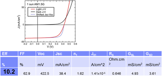
Figure 18. Top: J–V data from 10.2% device. Table: performance values from 10.2% device (from [69] John Wiley & Sons. [© 2016 WILEY-VCH Verlag GmbH & Co. KGaA, Weinheim]).
Download figure:
Standard image High-resolution imagePerhaps most interestingly, it was observed that the efficiency of this device continued to increase with decreasing temperature to a peak value of 16.2% at and below 175 K (see figure 19) [69]. This is in contrast with what is typically observed for CZTS,Se where the efficiency drops dramatically at these temperatures due to significant charge trapping in defect states.

Figure 19. Left: efficiency as a function of temperature showing a maximum of 16% at temperatures below 175 K. Right: Voc as a function of temperature showing the extrapolation to 0 K to be well below the actual expected band gap for both CZTS,Se and ACZTS,Se (from [69] John Wiley & Sons. [© 2016 WILEY-VCH Verlag GmbH & Co. KGaA, Weinheim]).
Download figure:
Standard image High-resolution image
That 16% efficiencies can be achieved, albeit at low temperatures, indicates that alloying may indeed be the correct approach to achieving higher efficiencies in kesterite absorber based PV devices.
Future directions
As of this writing, the need for energy harvesting strategies for autonomous devices is at an all-time high. Devices that will integrate an ultra-low power processor, sensors and communications are at the heart of the Internet-of-Things (IoT) and will require a power source for long term functioning in places where wall plug power is not available [77]. Since these devices will be deployed in the environment at large they must be non-toxic and environmentally benign; CZTS,Se based PV devices fit this profile.
An important question is whether CZTS,Se based PV devices, coupled with an appropriate battery would function properly under both 1 sun and indoor light intensities. Typical office illumination corresponds to ∼10−3 suns and while output current depends linearly on light intensity, Voc depends on ln(Jsc/Jo) where Jo is reverse saturation current that is typically a very small number (∼10−10 A m−2). Importantly, the achievable voltage at low light levels is strongly dependent upon the shunt resistance of the solar cell. The simple solar cell model involves a diode in parallel with a resistor called a shunt. When this resistance is a low value there is a considerable drop in voltage across this 'shunt resistor' but if the resistance is high, typically >1000 Ω cm2 (where we use current density in A cm–2) then Voc will drop slowly. Any drop across the shunt resistor represents a parasitic loss of voltage in the device. At present, we typically fabricate high voltage PV devices with shunt resistances ranging from 800–1500 Ω cm2 which is adequate to retain a substantial voltage even at low light levels.
Requirements to power microprocessors, sensors and even to charge a battery of course vary, but typical IoT autonomous devices would strive to operate at low power. If we consider the basic IoT device to consist of a low power microprocessor/controller, a sensor and communications we can estimate the power and voltage requirements. A key aspect is the threshold voltage required to run the microprocessor which can be 1 V or lower. Since the active power consumed by the processor is given by CV2F, where C is the capacitance, V the operating voltage and F the clock frequency, running at the lowest possible voltage can dramatically reduce the power. In addition to running a microprocessor at low voltage, clock frequencies can be reduced to match the properties of the events being measured, and periodic measurements, where the device is in its quiescent state until measurements must be made further reduce power requirements. Sensors are another critical area. An electrochemical sensor monitoring pollution or toxic gases can draw 100–500 μA at 1–2 V. Communicating the data generated by the sensor and analyzed by the microprocessor to a central hub or other nearby devices might be accomplished with a modulated light-emitting-diode that would operate at 1 V but might draw mA currents in short bursts [77]. Coupling a battery with appropriate chemistry to provide lower voltage is also a key element. A typical commercially available Li-ion battery produces 3.6 V and lowering this to ∼1–2 V requires energy consuming voltage regulation circuitry. Batteries typically supply a roughly constant voltage until depleted. Hence it is advantageous to select a battery chemistry that matches the low voltage needs of an autonomous device, bypassing the need for voltage regulation circuitry. PV devices operating at or slightly above the battery charging voltage would recharge this battery, slowly under low light conditions and more rapidly under higher illumination.
To achieve the highest voltages with CZTS,Se based PV, annealing CZTS,Se in excess S during the HB replaces Se within the lattice with S, increasing the band gap and hence achievable device voltage. Devices can be fabricated that yield a Voc in excess of 650 mV with high current and efficiencies. These individual cells can be serially connected to produce monolithic devices consisting of multiple units to achieve higher voltages; in our experiments we have serially connected up to 9 devices on a single substrate that combine to provide >5.5 V and 23–25 mA cm−2 under 1 sun. Performance of amorphous Si, a competing technology operating at the 10% efficiency level provides an alternative material [78]. But the advantages for CZTS,Se include a solution deposition process amenable to extremely inexpensive manufacturing, deposition on flexible and hence conformable substrates and it can be scaled to very small dimensions where high voltage may be required (as in threshold voltages for microprocessors) but where the reduced current capabilities are not an issue or trickle charging of a battery is sufficient. Furthermore the exfoliation of CZTS,Se devices providing access to the back contact suggests that integration with a battery may be achievable in an extremely compact assembly. As more autonomous devices are deployed in the field, powering them over potentially years of service will become a critical need and PV based devices, coupled with energy storage systems such as batteries, that are small, efficient and inexpensive will fill this need.
Acknowledgments
The information, data, or work presented herein was funded in part by an agency of the United States Government. Neither the United States Government nor any agency thereof, nor any of their employees, makes any warranty, express or implied, or assumes any legal liability or responsibility for the accuracy, completeness, or usefulness of an information, apparatus, product, or process disclosed, or represents that its use would not infringe privately owned rights. Reference herein to any specific commercial product, process, or service by trade name, trademark, manufacturer, or otherwise does not necessarily constitute or imply its endorsement, recommendation, or favoring by the United States Government or any agency thereof. The views and opinions of authors expressed herein do not necessarily state or reflect those of the United States Government or any agency thereof.